Note: Descriptions are shown in the official language in which they were submitted.
CA 02364201 2001-12-03
Optical Interference Member for Matrix Displays
Field of the Invention
The present invention relates generally to active matrix displays or other
patterned
displays, and more particularly relates to patterned displays incorporating
filters or other
means to reduce reflectance of ambient light.
Background of the Invention
Many display technologies are well known and such technologies are continuing
to advance rapidly. For example, modern active matrix display technology can
be
incorporated into display devices that are relatively lightweight, thin, and
which provide
high resolution and richly coloured pictures for televisions, computer
monitors, and more
generally, for a wide variety of display devices that can be incorporated into
appliances
like personal digital assistants and cellular telephones. While current active
matrix
displays can be expensive, it is expected that further research will result in
advances that
will can reduce the costs of such displays and lead to overall greater usage
of active
matrix display devices.
Active matrix displays are proving to be superior in many ways to older
display
technologies such as cathode-ray tubes ("CRT"). However, the problem of
"glare" off of
active matrix displays is also a concern, just as with older CRTs. "Glare" can
be defined
as ambient light that is reflected off of the device and back towards the
viewer, thereby
reducing the contrast and overall performance of the display device.
Thus, it is also known to incorporate technology to reduce reflectance into
displays and thereby improve their performance. In the case of active matrix
displays (or
indeed, any other type of pixellated display) it is known to use a black
matrix of filtering
material. The black matrix is mounted in a complementary fashion to the matrix
of pixels
in the display, such that the black matrix is a generally continuous filter
that surrounds
each pixel. Black matrices are described in a number of patents and patent
applications,
CA 02364201 2001-12-03
and method for preparation of same", EP 716 334 to Steigerwald ("Steigerwald
#1");
"Transmissive Display Device Having Two Reflection Metallic Layers of
Differing
Reflectances", US 6,067,131 to Sato ("Sato"); "Anti-reflector black matrix
display
devices comprising three layers of zinc oxide, molybdenum and zinc oxide", US
5,570,212 to Steigerwald ("Steigerwald #2"); "Anti-reflector Black Matrix
Having
Successively A Chromium Oxide Layer, a Molybdenum Layer And a Second
Chromium Oxide Layer", US 5,566,011 to Steigerwald ("Steigerwald #3"); and,
"Low
Reflectance Shadow Mask", US 5,808,714 to Rowlands et al. ("Rowlands"). One
particular disadvantage to Steigerwald #1, Steigerwald #2 Steigerwald #3 and
Rowlands is that they are confined to black matrix structures having specific
sets of
materials. A more general discussion of applying a black matrix as applied to
a
display having colour filters is found in US Patent 5,587,818 to Lee ("Lee").
However, such prior art black matrix structures are not always useful or
practical to incorporate into display devices. For example, prior art black
matrix
structures are frequently formed as a separate unit from the display, thereby
eventually
requiring the assembly of the black matrix structure to the display structure,
such as
by mounting the black matrix structure to the front of the display.
It is also known to use optical interference to reduce reflectance in various
thin
film display technologies, such as electroluminescent devices ("ELD"s). For
example, reducing reflectance of ambient light can be achieved by using
additional
thin film layers sandwiched between one or more layers of the ELD, which are
configured to achieve destructive optical interference of the ambient light
incident on
the display, thereby substantially reducing reflected ambient light. Optical
interference technology is discussed in detail in U.S. Patent 5,049,780 to
Dobrowolski
et al., ("Dobrowolski") and the applicant's copending U.S. Application
09/361,137
and filed on July 27, 1999, to Hofstra et al. ("Hofstra") The contents of both
of these
documents are incorporated herein by reference. In addition to enhancing
contrast, the
optical interference contrast enhancement apparatuses discussed in Dobrowolski
and
Hofstra also reduce pixel blooming and solar loading - another advantage of
such
apparatuses over certain other types of anti-reflection technologies.
The teachings of Dobrowolski and Hofstra can be useful in reducing
reflectance of ambient light in ELDs, either organic or inorganic. The
teachings of
2
CA 02364201 2001-12-03
Dobrowolski and Hofstra can also be used to reduce reflectance in active
matrix or
other patterned displays, when the optical interference technology taught
therein is
incorporated in conjunction with the ELD. However, the teachings of
Dobrowolski
and Hofstra are not directed to active matrix technologies and therefore
devices
requiring contrast enhancement will generally rely upon prior art black matrix
technologies, such as that taught in Steigerwald #1, Steigerwald #2
Steigerwald #3,
Rowlands or Sato.
Summary of the Invention
It is therefore an object of the present invention to provide a optical
interference
member which obviates or mitigates at least one of the disadvantages of the
prior art.\
In an aspect of the invention, there is provided a display device comprising a
plurality of light emitting members patterned to present an image to a viewer
and a
plurality of bus lines that are operable to provide an electrical signal to
each of the
light emitting members. At least a portion of the bus lines are in
substantially the
same viewing plane as the image. The display further comprises an optical
interference member intermediate the viewer and the bus lines, the optical
interference
member is patterned to substantially correspond with at least a portion of one
of the
bus lines. The optical interference member is operable to reduce a reflection
of
ambient light back towards a viewer using optical interference.
Brief Description of the Drawings
The present invention will now be described, by way of example only, with
reference to certain embodiments shown in the attached Figures in which:
Figure 1 is a schematic representation of a partial cross-section of a portion
of
an active matrix display in accordance with an embodiment of the invention;
Figure 2 is a partial front view along the line II-II of Figure 1;
3
CA 02364201 2001-12-03
Figure 3 is a schematic representation of a specific implemenation of the
optical inteference member shown in Figure 1; and,
Figure 4 is a schematic representation of a partial cross-section of a portion
of
an active matrix display in accordance with ano embodiment of the invention.
Detailed Description of the Invention
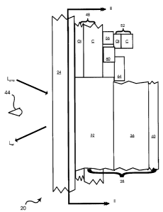
Referring now to Figures l and 2, an active matrix display in accordance with
an embodiment of the invention is indicated generally at 20. As seen in Figure
1,
display 20 includes a substrate 24 made from glass or any other suitable
substrate
material. Display 20 includes a plurality of light emitting pixels that are
deposited
onto substrate 24. Figures 1 and 2 both show a single pixel indicated at 28.
In turn
each pixel 28 is comprised of a front electrode 32, a light emitting member 36
and a
rear electrode 40. The exact configuration of each pixel 28 is not
particularly limited,
and thus can be based on inorganic electroluminescent display technology,
organic
electroluminescent display, plasma display technology, liquid crystal display
technology or the like. Depending on the type of pixel 28, it will thus be
understood
that the exact materials and/or configurations of electrode 32, light emitting
member
36 and rear electrode 40 will be chosen correspondingly. Furthermore, pixel 28
may
include additional layers, as required, such as work function matching layers
and/or
transport layers where light emitting member 36 is based on an organic
electroluminescent display material. Alternatively, where member 36 is based
on an
inorganic electroluminescent display material, then dielectric layers may be
added. It
is thus to be understood that, in general, pixel 28 can be based on a variety
of
technologies, and accordingly, the formations of such pixels 28 on substrate
24 will be
performed according to known techniques specific to the type of technology.
Such
formations may include, for example, successively depositing both light
emitting
member 36 and rear electrode 40 as two continuous layers along the entirety of
substrate 24, thereby covering the remaining components of display 20.
Accordingly,
pixel 28 is operable to create emitted light, indicated as Lem in Figure 1,
towards a
viewer 44 located in front of display 20.
Regardless of the technology used for pixel 28, it is presently preferred for
the
present embodiment that front electrode 32 be formed from a transmissive
conducting
5 4
CA 02364201 2001-12-03
material, such as indium tin oxide (ITO). Rear electrode 40 can be formed from
either
a transparent or reflecting metal, depending on whether display 20 is a
transparent
display.
A plurality of gate bus lines 48 perpendicular to a plurality of source bus
lines
52 form a matrix on display 20. While gate bus lines 48 are deposited directly
onto
substrate 24, source bus lines 52 are deposited behind gate bus lines 48.
Thus, source
bus lines 52 and substrate 24 sandwich gate bus lines 48. Intersections of bus
lines 48
and 52 are separated by an insulator 56 to electrically isolate each set of
lines 48 and
52. Accordingly bus lines 48 and 52 surround each pixel 28.
Gate bus lines 48 are attached to the gate input of a transistor 60 (or other
switching means) respective to each pixel 28. Similarly, source bus lines 52
are
attached to the source input of transistor 60. A drain 64 interconnects
transistor 60
and front electrode 32. (While not required, it is contemplated that drain 64
can also
be coated with an optical interferemence member, (not shown)). Those of skill
in the
art will now recognize that device 20 will include appropriate electronics,
generally
along its periphery, which can individually address each pixel 28, and
accordingly
such electronics are operable to activate each pixel 28 by applying the proper
electrical signals to the gate and source of the transistor 60 respective to
pixel 28.
Gate bus lines 48 and source bus lines 52 are each composed of an optical
interference member OI and a conducting layer C. As described above,
conducting
layer C allows each line 48 and 52 to carry electrical signals to each
transistor 60 in
the usual manner. However, as will be explained in greater detail below,
optical
interference member OI cooperates with conducting layer C in order to reduce
reflections back towards viewer 44 of ambient light incident upon display 20.
Ambient light is indicated as Lamb in Figure 1, whereas reflected light is
indicated as
Lref In Figure 1.
The materials, composition, and thicknesses of optical interference member OI
and conducting layer C are chosen to allow conducting layer C to perform its
conducting duties, while causing ambient light Lamb to destructively interfere
with
itself, upon its reflection off of bus lines 48 and 52 such that the overall
amount of
reflected light L~ef back towards viewer 44 is reduced.
5
CA 02364201 2001-12-03
Referring now to Figure 3, a presently preferred configuration of optical
interference member OI and conducting layer C for each bus line 48 and 52 is
shown
in substantially the same view as Figure 1, but in isolation from the other
components
of device 20. According to Figure 3, each optical interference member OI is
comprised of a semi-absorbing layer 70 which is oriented the closest towards
viewer
44. Optical interference member OI is also comprised of a substantially
transparent
layer 74 that is mounted behind semi-absorbing layer 70. Finally conducting
layer C
is mounted behind semi-absorbing layer 70 of optical interference member OI.
Each layer 70, 74 of optical member OI and conducting layer C, of each set of
bus lines 48 and 52 (separated by insulator 56) can be successively deposited
as
complete layers on substrate 24 in the order shown in Figure 3, and then the
actual bus
lines 48 and 52 can be etched into the above-described matrix pattern using
known
techniques. Other techniques for forming each bus line 48 and 52 according to
the
configuration shown in Figure 3 will occur to those of skill in the art.
The thickness and material of semi-absorbing layer 70 is chosen so that semi-
absorbing layer 70 is partially reflective, partially absorbing and partially
transmissive
of ambient light La",b Accordingly, a portion of ambient light La",b incident
on layer 70
is partially reflected off of layer 70, while a remaining portion passes into
semi-
absorbing layer 70. A portion of the light passing through layer 70 is
absorbed, being
dissipated as a small amount of heat. The remaining amount of light is passed
directly
through layer 70. The extinction coefficient and the thickness of the material
of layer
70 is chosen so that the reflection from layer 70, neglecting optical
interference, is
preferably at least about thirty-five percent. Similarly, the transmissivity
through layer
70 should also be about thirty-five percent. The remaining amount of light is
absorbed and dissipated as a small amount of heat. It is presently preferred
that a
wavelength of about SSOnm be chosen (roughly the middle of the spectrum of
visible
light) when choosing the above extinction coefficient, thickness and/or
material of
layer 70. One suitable material and thickness for layer 70 is Chromium or
Aluminum,
having a thickness of about 100 t~ . As an alternative magnesium silver
(Mg:Ag)
having a thickness of about 185 ~ can also be used for layer 70. Other
suitable
materials (and for which appropriate thicknesses can be chosen) for layer 70
can
include inconel or nickel. Still further materials for layer 70 can include
Cu, Au, Mo,
6
CA 02364201 2001-12-03
Ni, Pt, Rh, Ag, W, Co, Fe, Ge, Hf, Nb, Pd, Re, V, Si, Se, Ta, Y, Zr. Still
other
material and thicknesses for layer 70 will occur to those of skill in the art.
The remaining amount of light which is transmitted completely through layer
70, then passes through substantially transparent layer 74. The extinction
coefficient
and the thickness of the material of layer 74 is chosen such that transmission
through
layer 74 (using the same wavelength of about SSOnm as used to select layer 70)
is
greater than about eighty percent, but preferably at least about ninety
percent. One
suitable material and thickness for layer 74 is indium tin oxide (ITO) having
a
thickness of about 540 ~. Other suitable materials (and for which appropriate
thicknesses can be chosen) for layer 74 can include Aluminum Silicon Monoxide
or
Chromium Silicon Monoxide. Additional materials for layer 74 can include
A1z03,
SiOz, ZrOz, HfOz, Scz 03, TiOz, Laz03, MgO, Taz O5, ThOz, Y203, CeOz, A1F3,
CeF3,
Na3 A1F6, LaF3, MgFz, ThF4, ZnS, Sbz 03, Biz 03, PbFz, NdF3, Ndz O~,
Pr60~~,
SiO, NaF, ZnO, LiF, Gd03. Still further materials and thicknesses for layer 74
will
occur to those of skill in the art.
Thus, the light that passes through layer 74 to reach conductor C is reflected
off of conductor C. Thus, conductor C is preferably a reflective material,
such as
Aluminum, having a thickness such that conductor C is not transparent and is
suitable
for carrying electrical signals along its respective bus line 48 or 52.
The light that is reflected off of conductor C then passes back through layer
74, again through layer 70 (where still a further portion of it is absorbed)
and then the
final remainder of the light reflected off of conductor C exits layer 70, at
which point
it is out of phase with the light originally reflected off of layer 70.
Because these two
reflections are out of phase, they destructively interfere, thereby reducing
reflected
light Lee back towards viewer 44. The inventors believe that, (if desired)
through
careful selection of materials, thicknesses and extinction coefficients for
optical
interference member OI, the two reflections off of layer 70 can have
substantially the
same intensities and be about one-hundred-and-eighty degrees out of phase,
thereby
substantially eliminating reflected light Lref~
While the foregoing describes an optical interference member OI having two
layers, other configurations of optical interference members OI are within the
scope of
7
CA 02364201 2001-12-03
the invention. Additional, or fewer layers can be used to form optical
interference
members OI as desired. For example, it is contemplated that optical
interference
member OI could be formed from a single layer of semi-absorbing material. The
thickness, material and index of refraction are chosen in order to achieve
destructive
optical interference of reflected ambient light La",b. Such materials,
thicknesses and
indeces of refraction are discussed in detail in the Applicant's copending
application
entitled "Contrast Enhancement Apparatus", filed in the Canadian Patent Office
on
July 04, 2001, and bearing application number 2,352,390, the contents of which
are
incorporated herein by reference.
Referring now to Figure 4, a display in accordance with another embodiment
of the invention is indicated generally at 20a. Display 20a is substantially
identical in
construction and operation to display 20 of Figure l, except that display 20a
includes
two optical interference members, OIa and OIb which are affixed to both sides
of each
conductor C. The optical interference member OIa affixed to the side of each
1 S conductor C that is closest to substrate 24 is identical to the optical
interference
member OI in display 20 of Figure 1. However, the second optical interference
member OIb affixed to the side of each conductor C that is closest to rear
electrode 40
is substantially identical in structure to optical interference OIa, but
operates to reduce
pixel blooming, as light which is emitted from the back of light emitting
members 32
which are adjacent to the light emitting member 32 shown in Figure 4 can be
eliminated by optical interference member OIb. Those of skill in the art will
now
recognize that optical interference member OIb can be constructed from one or
more
layers of material, as previously described, excepted that optical
interference member
OIb is modified so that it reduces light that is incident from the side of
display 20a that
is opposite to substrate 24.
Pixel blooming from a second light emitting member (not shown) that is
adjacent to the light emitting member 32 is represented with the arrows marked
"LemA" in Figure 4. This pixel blooming emitted light LemA is thus shown
reflecting
off of rear electrode 40, and then striking optical interference member OIb of
source
bus line 52. Thus, optical interference member OIb is operable to reduce
emitted light
LemA using destructive interference, thereby reducing the amount of emitted
light
Le",A that passes through the front electrode 32 shown in Figure 4.
8
CA 02364201 2001-12-03
While only specific combinations of the various features and components of
the present invention have been discussed herein, it will be apparent to those
of skill
in the art that desired subsets of the disclosed features and components
and/or
alternative combinations of these features and components can be utilized, as
desired.
For example, other display technologies can be instead of light-emtting
pixels.
Instead, each pixel could be a shutter means that passes light emitted from a
back light
when the pixel is activated.
Furthermore, while the embodiments herein have referred to pixellated
displays, it is to be understood that other patterned displays are within the
scope of the
invention.
Furthermore, it is to be understood that the teachings herein can be modified
to
work with bottom emission or top emission active matrix displays.
In addition, in the embodiment shown in Figure 1, it is contemplated that
optical interference member OI of line 52 can be made from an insulating
material
and thereby obviate the need for insulator 56, provided enough of conducting
layer C
of line 52 is left exposed to make the required contact with transistor 60.
Furthermore, the enough herein can be used in conjunction with the optical
inteference members taught in Dobrowlowski and/or Hofstra.
The present invention provides a novel optical interference member that is
integrally formed over the bus lines of an active matrix or other patterned
display. By
coating the otherwise reflective bus lines with the optical interference
member,
unwanted ambient light towards the viewer can be reduced, while allowing the
emitted light to travel towards the viewer without having to pass through the
filter.
Additionally, in certain embodiments, the integral formation the bus lines
with the
optical interference member can offer simplified manufacturing techniques,
obviating
the need for forming a black matrix separately from the conducting bus lines.