Note: Descriptions are shown in the official language in which they were submitted.
CA 02364464 2001-09-07
WO 00/54398 PCT/US00/04872
GENERAL SELF-DRIVEN SYNCHRONOUS RECTIFICATION
SCHEME FOR SYNCHRONOUS RECTIFIERS
HAVING A FLOATING GATE
CROSS-REFERENCE TO RELATED APPLICATIONS
The following U.S. Patent Application is commonly assigned and is incorporated
herein by reference:
Patent No. Serial No. Inventor Title
TBD 09/209,733 Farrington, et al. Self Driven Synchronous
Rectification Scheme
TECHNICAL FIELD
This invention relates generally to power converter circuits, and more
particularly
to self driven synchronous rectifiers easily adapted to all types of circuit
topologies.
BACKGROUND OF THE INVENTION
As logic integrated circuits (ICs) have migrated to lower working voltages in
the
search for lower power consumption and higher operating frequencies, and as
overall
system sizes have continued to decrease, power supply designs with smaller
size and
higher efficiency are in demand. In an effort to improve efficiencies and
increase power
densities, synchronous rectification has become necessary for these type of
applications.
Synchronous rectification refers to using active devices such as the MOSFET as
a
-1-
CA 02364464 2001-09-07
WO 00/54398 PCT/US00/04872 .
replacement for Schottky diodes as rectifier elements in circuits to reduce
conduction
power losses in the secondary rectifiers. Recently, self driven synchronous
schemes have
been widely adopted in the industry as the desired method for driving the
synchronous
rectifiers in DC/DC modules for output voltages of 5 volts and below. Self
driven
synchronous schemes provide a simple, cost effective and reliable method of
implementing synchronous rectification.
Most of these schemes are designed to be used with a very particular set of
topologies commonly known as "D, 1-D" (complementary driven) type topologies.
See
Cobos, J.A., et al., "Several alternatives for low output voltage on board
converters",
IEEE APEC 98 Proceedings, at pp. 163-169. See also U.S. Patent 5,590,032
issued on
Dec. 31, 1996 to Bowman et al. for a Self synchronized Drive Circuit for a
Synchronous
Rectifier in a Clamped-Mode Power Converter, and U.S. Patent 5,274,543 issued
on Dec.
28, 1993 to Loftus entitled Zero-voltage Switching Power Converter with
Lossless
Synchronous Rectifier Gate Drive. In these types of converters, the gate of
the devices is
referenced to ground, and the power transformer signal in the secondary
winding has the
correct shape and timing to directly drive the synchronous rectifiers with
minimum effort.
Furthermore, the rectifier is configured to insure the synchronous rectifier
gate signals do
not float relative to secondary ground and are easy to drive. Figure 1 shows
an example
of this family of converters, with an active clamp forward circuit 10 and self
driven
-2-
CA 02364464 2001-09-07
WO 00/54398 PCT/US00/04872
synchronous rectification provided by synchronous rectification circuitry 12
comprising
two synchronous rectifiers .SQ1 and SQ2 coupled between the secondary winding
of the
transformer 18 and the output, Vo"~. As shown in Figure 2, the transformer
signal 20 for
these types of converters has a square shape with two very recognizable
intervals, each
corresponding to the "on" time of one of the synchronous rectifiers SQ1 and
SQ2.
In topologies such as the hard-switched half bridge (HB), the full-bridge (FB)
rectifiers, and the push-pull topologies and non-"D, 1-D" type topologies
(e.g. clamp
forward with passive reset), the transformer voltage has a recognizable zero
voltage
interval, making it undesirable to implement self driven synchronous
rectification. As a
result, it is necessary to use an external drive circuit with these circuit
topologies.
Changing the placement of the synchronous rectifiers relative to the
transformer to
simplify the driving scheme may result in a floating transformer winding with
respect to
ground, which generally increases common mode current between the primary and
secondary circuits, causing increased EMI noise. Rectifier circuits employing
synchronous rectification generally are reconfigured away from the EMI-
preferred
configuration.
What is needed in the art is a circuit and method for providing synchronous
rectification for the secondary side of a transformer that is suitable for use
with a wide
-3-
CA 02364464 2001-09-07
WO 00/54398 PCT/US00/04872
range of circuit topologies and has low EMI noise.
-4-
CA 02364464 2001-09-07
WO 00/54398 PCT/LTS00/04872 .
SLTNINIARY OF THE INVENTION
The present invention achieves technical advantages as a self driven
synchronous
rectification scheme with synchronous rectifiers having a floating gate. The
scheme may
be easily adapted to all type of topologies, including hard-switched HB, FB
and push-pull
converters, for which no efficient self driven synchronous rectification
scheme was
previously available.
The present invention is a self driven synchronous rectifier circuit for a
power
converter, the circuit including a first transformer having a primary winding
and a
secondary winding, the secondary winding having a first terminal and a second
terminal.
A first synchronous rectifier is coupled to the first transformer secondary
winding first
terminal and has a control terminal floating relative to ground. A first drive
circuit is
coupled to the first synchronous rectifier floating control terminal and
controls the first
synchronous rectifier. A first control signal is coupled to the first drive
circuit, wherein
the first control signal controls the first drive circuit as a function of a
voltage polarity
reversal across the first transformer. The first control signal may be a
signal from the
first transformer secondary winding second terminal, or may be a signal from a
second
transformer secondary winding terminal of a signal transformer.
The circuit may also further include a second synchronous rectifier coupled to
the
-5-
CA 02364464 2001-09-07
WO 00/54398 PCT/US00/04872
first transformer secondary winding second terminal having a control terminal
floating
relative to ground, and a second drive circuit coupled to the second
synchronous rectifier
floating control terminal and controlling the second synchronous rectifier. A
second
control signal may be coupled to the second drive circuit, wherein the second
control
signal controls the second drive circuit as a function of a voltage polarity
reversal across
the first transformer. The first drive circuit may include a first switch and
a second
switch in a totem pole arrangement, and the second drive circuit may include a
third
switch and a fourth switch in a totem pole arrangement, where the switches are
MOSFETs.
Also disclosed is a method of rectifying a varying voltage from a power
converter
using a self driven synchronous rectifier circuit with a first transformer
having a primary
winding and a secondary winding, where the secondary winding has a first and
second
terminal. The method includes the steps of providing a varying signal to the
primary
winding of the first transformer, and a first synchronous rectifier having a
control
terminal conducting current via the first transformer secondary winding, where
the
control terminal floats relative to ground. A first drive circuit controls the
first
synchronous rectifier, and a first control signal controls the first drive
circuit as a function
of a voltage polarity reversal across the first transformer. A second
synchronous rectifier
having a control terminal conducts current via the first transformer secondary
winding,
-6-
CA 02364464 2001-09-07
WO 00/54398 PCT/US00/04872
and the control terminal floats relative to ground. A second drive circuit
controls the
second synchronous rectifier, and a second control signal controls the second
drive circuit
as a function of a voltage polarity reversal across the first transformer.
BRIEF DESCRIPTION OF THE DRAWINGS
The above features of the present invention will be more clearly understood
from
consideration of the following descriptions in connection with accompanying
drawings in
which:
Figure 1 illustrates a prior art active clamp forward converter with self
driven
synchronous rectification;
Figure 2 illustrates typical transformer voltages for a "D, 1-D" type
converter
shown in Figure 1;
Figure 3A shows a prior art clamp forward circuit with passive reset;
Figure 3B shows typical secondary transformer voltage waveforms for the prior
art circuit shown in Figure 3A;
CA 02364464 2001-09-07
WO 00/54398 PCT/US00/04872
Figure 4 illustrates a clamp forward circuit with passive reset utilizing a
first
embodiment of the present invention;
Figure 5 shows voltage waveforms of the self driven synchronous rectifier
circuit
of the first embodiment of the present invention for a clamp forward circuit
with passive
reset of Figure 4;
Figure 6 shows a second embodiment in use with a half wave rectifier with the
present invention and external inductors;
Figure 7 illustrates a third embodiment of the present invention configured
for a
full-wave rectifier;
Figure 8 shows a fourth embodiment of the present invention with a full-wave
rectifier and alternative gate connections of the driving circuits;
Figure 9A illustrates a fifth embodiment of the present invention configured
for a
full wave rectifier, with an inductor coupled in series with the transformer
second wining
center tap and the output return voltage;
_g_
CA 02364464 2001-09-07
WO 00/54398 PCT/US00/04872
Figure 9B illustrates a sixth embodiment of the present invention configured
for a
full wave rectifier, with an alternative configuration of the diodes across
the drive
circuits;
Figure l0A shows a seventh embodiment of the present invention configured for
an active clamp forward circuit;
Figure l OB shows an eighth embodiment of the present invention configured for
an active clamp forward-flyback circuit;
Figure 11 illustrates a ninth embodiment of the present self driven
synchronous
rectification scheme for a full-wave rectifier with optional current-limiting
resistors;
Figure 12 shows a tenth embodiment of the present self driven synchronous full-
wave rectifier having optional gate voltage limiters;
Figure 13 shows synchronous rectifier current waveforms for hard-switched push-
pull type topologies;
-9-
CA 02364464 2001-09-07
WO 00/54398 PCT/~JS00/04872 .
Figure 14 shows an eleventh embodiment of the present invention with saturable
inductors;
Figure 15 illustrates waveforms for the eleventh embodiment having saturable
inductors; and
Figure 16 shows a twelfth embodiment configured for use with a signal
transformer.
Corresponding numerals and symbols in the different figures refer to
corresponding parts unless otherwise indicated.
DETAILED DESCRIPTION OF PREFERRED EMBODIMENTS
The following is a description of the structure and method of the present
invention. Prior art circuits will be discussed first, followed by a
description of several
preferred embodiments and alternatives of the present invention, and a
discussion of the
advantages.
The prior art synchronous rectifier shown in Figure 1 is undesirable for use
with
some circuit topologies, such as the hard-switched hall=bridge (HB), the full-
bridge (FB)
rectifiers, and the push-pull topologies and non-"D, 1-D" type topologies
(e.g. clamp
-10-
CA 02364464 2001-09-07
WO 00/54398 PCT/US00/04872
forward with passive reset). The transformer voltage has a recognizable zero
voltage
interval, making it undesirable to implement self driven synchronous
rectification. As a
result; it is necessary to use an external drive circuit with these circuit
topologies. In
addition, a dissipative snubber is usually required, to limit the voltage
stress across the
synchronous rectifiers and dampen voltage oscillation.
Furthermore, using the transformer voltage to drive the synchronous rectifiers
for
these circuit topologies results in conduction of the parasitic anti-parallel
diode of the
MOSFETs used for synchronous rectifiers SQ1 and SQ2 for a significant portion
of the
freewheeling interval, negatively affecting the efficiency of the module,
which is
undesired. Some self driven implementations for the resonant reset forward
have been
reported. See Murakami, N. et al., "A Highly Efficient, Low-profile 300 W
Power Pack
for Telecommunications Systems", IEEE APEC 1994 Proceedings, at pp. 786-792
and
Yamashita, N. et al., "A Compact, Highly Efficient 50 W On Board Power Supply
Module for Telecommunications Systems", IEEE APEC 1995 Proceedings, at pp. 297-
302. In these implementations, the resonant reset interval has been adjusted
to provide
the correct gate-drive signal during the freewheeling interval. In another
design, an
implementation of self driven rectification is shown for a two-switch forward
converter.
See Nakayashiki, Y. et al., "High-Efficiency Switching Power Supply Unit with
Synchronous Rectifier," IEEE INTELEC 1998 Proceedings, at pp. 398-403.
-11-
CA 02364464 2001-09-07
WO 00/54398 PCT/US00/04872
Changing the placement of the synchronous rectifiers of the prior art circuit
of
Figure 1 so they are referenced to ground, using the transformer signal to
directly drive
the synchronous rectifiers, is disadvantageous, because the transformer
winding then
floats with respect to ground. Generally, a rectifier with a floating
transformer generates
increased common mode currents between the primary and secondary circuits,
which
results in increased ElectroMagnetic Interference (EMI). The preferred, EMI
quiet,
secondary side circuit configuration requires that at least one of the
synchronous rectifiers
have a gate drive signal that floats relative to ground. This generally
increases the
complexity of the driving circuitry.
Figure 3A shows a prior art clamp forward circuit 22 with passive reset and
Figure 3B shows the associated typical secondary transformer voltage waveform
28. If
traditional self driven synchronous schemes are used with this topology, it
can be shown
that the synchronous rectifier which conducts during the freewheeling stage
will turn off
before this stage ends in time period 30. In this case the anti-parallel diode
of the
MOSFET conducts, increasing the losses. In order to obtain high efficiency, it
is
necessary for this MOSFET to conduct during the entire freewheeling stage.
Furthermore, without rearranging the configuration of the secondary circuit, a
floating
gate drive would be needed to drive the synchronous rectifier replacing diode
D3.
-12-
CA 02364464 2001-09-07
WO 00/54398 PCT/US00/04872 .
Traditional self driven synchronous rectifier schemes use the voltage
developed
by the transformer to turn-on the corresponding synchronous rectifier, and
when this
voltage decays to zero, the synchronous rectifier is turned off. However,
rectifiers
(diodes) do not operate in this manner. Generally, diodes require voltage of
the opposite
polarity to turn off. Therefore, traditional driving schemes provide a
practical solution in
a limited number of circuit configurations.
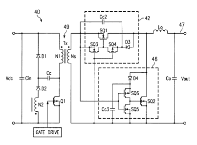
The present invention achieves technical advantages as a self driven
synchronous
rectifying scheme utilizing the same principles as a silicon diode and may be
easily
implemented in all types of circuit topologies configurations. The present
invention is a
synchronous rectifier scheme 40 with synchronous rectifiers SQl and SQ2 having
gates
that float relative to ground, as shown in a first embodiment in Figure 4.
Transformer 49
has a primary winding and a secondary winding. Circuit 42 is coupled to a
first end of
the transformer 49 secondary winding and comprises two small switches SQ3 and
SQ4
coupled to the gate of the synchronous rectifier SQl . Circuit 42 also
includes a floating
supply voltage comprised of Cc2 and D3. Likewise for circuit 46, two small
switches
SQS and SQ6 are coupled to the gate of synchronous rectifier SQ2. Circuit 46
also
includes a floating supply voltage comprised of Cc3 and D4. Preferably, an
inductor Lo is
coupled in series between the circuit 46 and an output voltage terminal 47 to
smooth
-13-
CA 02364464 2001-09-07
WO 00/54398 PCT/US00/04872 .
current ripples, and a capacitor Co is coupled across the rails to smooth the
voltage, as
shown.
Synchronous rectifiers SQ1 and SQ2 and switches SQ3, SQ4, SQS and SQ6
preferably comprise Field Effect Transistors (FETs), and more preferably
comprise Metal
Oxide Semiconductor FETs (MOSFETs), with the switch MOSFETs SQ3, SQ4, SQS and
SQ6 being smaller than the synchronous rectifier MOSFETs SQl and SQ2. The two
smaller switches SQ3, SQ4, and SQS, SQ6, for each synchronous rectifier SQ1
and SQ2,
respectively, form first and second totem-pole drive circuits that each float
relative to
ground, and are adapted to control the respective synchronous rectifiers SQl
and SQ2. In
particular, in accordance with the present invention, the gates of the
synchronous
rectifiers SQl and SQ2 float relative to ground. Preferably, switches SQ3 and
SQ5 are
N-type MOSFETs, and switches SQ4 and SQ6 are P-type FETs.
A first control signal derived from the second terminal of the transformer 49
secondary winding controls the first drive circuit as a function of a polarity
reversal of a
voltage across the transformer 49. A second control signal derived from the
first terminal
of the transformer secondary winding controls the second drive circuit as a
function of a
polarity reversal of a voltage across the transformer 49. In this driving
scheme, the
synchronous rectifiers SQ1 and SQ2 are not turned off when the transformer
signal
-14-
CA 02364464 2001-09-07
WO 00/54398 PCT/US00/04872 .
vanishes to zero as in the traditional self driven scheme, but rather, are
turned off when
the transformer voltage switches polarity. The synchronous rectifiers SQl and
SQ2
remain on and conduct when the transformer signal vanishes to zero, in
contrast to the
traditional self driven schemes of the prior art. According to the present
invention,
synchronous rectifiers SQ1 and SQ2 are turned off when the transformer voltage
switches
polarity. Synchronous rectifiers SQ1 and SQ2 are turned on through their
respective
totem-pole drive circuit, and are turned off when the transformer voltage
switches
polarity through the respective totem-pole drive circuit.
Capacitors Cc 1 and Cc2 and diodes D3 and D4 generate the floating supply
voltages needed to drive SQ1 and SQ2. By implementing the floating supply
voltages in
this manner, an additional advantage is achieved in that diode D3 and
capacitor Ccl
clamps the voltage across synchronous rectifier SQl, and diode D4 and
capacitor Cc2
clamps the voltage across synchronous rectifier SQ2. Capacitors Ccl and Cc2
limit the
voltage stress across the synchronous rectifiers to approximately twice the
input voltage
reflected into the secondary side (~ 2*Vin*Ns/N1).
Generally, the interaction of the output capacitance of the synchronous
rectifiers
and the leakage inductance of the transformer result in increased voltage
stress across the
rectifiers. This increased voltage stress limits the type of devices that can
be used for the
-15-
CA 02364464 2001-09-07
WO 00/54398 PCT/US00/04872 .
synchronous rectifiers. In order to take full advantage of synchronous
rectification,
devices with the lowest possible Rds(on) are preferably used. Semiconductor
physics
dictate that lower voltage-rated devices typically have lower Rds(on).
Therefore, it is
important to minimize the increased voltage stress due to the interaction of
circuit
parasitics. The present invention minimizes the effect of these parasitic
effects by
clamping the voltage stress across the synchronous rectifiers with a capacitor
that has a
value much larger than the output capacitance of these devices. The energy
stored in the
clamp capacitors Cc2 and Cc3 is used in the present circuit to drive the
synchronous
rectifiers SQ1 and SQ2, respectively.
At first glance, this self driven synchronous rectifying scheme may seem to
have
a fundamental flaw. Refernng to the waveforms in Figure 5, at time T < to
rectifier SQl
is off (signal 52) and rectifier SQ2 is conducting (signal 54). The
transformer voltage is
shown at signal 56. At time T = to the primary switch Q1 turns on (signal 50)
and tries to
initiate a new switching cycle. Assuming an ideal transformer 49 (no leakage
inductance
and no series resistance) and the absence of all parasitics in the secondary
circuit, the
primary switch Ql turns on into a short circuit. The sequence is as follows:
at the time
when the primary switch Q1 turns on, the anti-parallel diode of rectifier SQ1
instantaneously tries to conduct with rectifier SQ2 still on, resulting in a
short formed
across the secondary winding of the transformer 49. Rectifier SQ2 needs the
voltage of
-16-
CA 02364464 2001-09-07
WO 00/54398 PCT/US00/04872 .
the transformer 49 to reverse polarity in order to turn off, but this voltage
cannot reverse
before rectifier SQ2 turns off. However, this concept assumes ideal components
and
circuit layout. Therefore, if stray inductances and resistances are
incorporated into the
discussion it can be easily shown (experimentally and by simulation) that at
switching
frequencies of several kilohertz, the stray inductances and resistances found
on a typical
converter layout allow enough voltage to develop in the secondary to turn off
rectifier
SQ2. Rectifier SQ1 turns on into a momentary "short circuit".
The driving scheme of the present invention results in "shoot through"
currents
(peak currents due to a short circuit) during switching transitions, which may
be
compensated for, as will be described herein. For the current levels and
switching
frequencies most board-mounted power modules are designed for, these shoot
through
currents are not severe. The shoot through currents result from turning on the
synchronous rectifiers SQ1 and SQ2 "late", and are less severe than the shoot
through
currents developed due to the reverse recovery effect intrinsic to all
synchronous
rectifiers when their parasitic anti-parallel diode is allowed to conduct, as
is the case in
traditional self driven synchronous schemes. The parasitic anti-parallel
diodes of the
MOSFETs used for synchronous rectifiers SQ1 and SQ2 are very slow and do not
turn
off fast enough in this type of application: therefore, shoot-through currents
are
generated. These currents can be very severe, particularly at full load,
compromising the
-17-
CA 02364464 2001-09-07
WO 00/54398 PCT/US00/04872
performance of the module. It is recognized that one of the effects that
prevents
synchronous rectification from being used at higher switching frequencies (>
500 kHz) is
the loss resulting from reverse recovery in the synchronous rectifiers SQ1 and
SQ2.
If shoot through currents interfere with the normal operation of the circuit,
optional external inductor LS 1 and/or LS2 may be added in series with
synchronous
rectifiers SQ1 and/or SQ2, respectively, and Lo, as shown in a second
embodiment of the
present invention in Figure 6. These external inductors LS 1 and LS2 are
preferably one-
turn fernte inductors that are allowed to saturate, or a more typical
saturable inductor
having square loop material. Using a saturable inductor minimizes the effect
of the
inductor on the overall performance of the circuit while eliminating shoot-
through
currents. Only one of the two inductors LS 1 and LS2 is required to limit the
shoot
through currents, because LS 1 and LS2 are effectively in series during the
switching
transitions. Furthermore, these external inductors LS 1 and LS2 are preferably
placed in
series with the clamping circuits Cc2 and D3, or Cc3 and D4, to avoid limiting
the
effectiveness of the clamping circuitry in reducing the voltage stress across
the
synchronous rectifiers SQl and SQ2.
The implementation of the present invention for use with a full-wave rectifier
is
similar to that of the half wave rectifier and is shown in a third embodiment
in Figure 7.
-18-
CA 02364464 2001-09-07
WO 00/54398 PCT/US00/04872 .
The center tap of the transformer 70 is coupled to a return voltage terminal,
with circuits
42 and 46 coupled to the transformer as described in Figure 4. In the
configuration
shown for a full-wave rectifier, the maximum voltage stress seen from gate to
source of
the N-type FETs SQ3 and SQS is approximately equal to 2*Vin*Ns/N1. The voltage
stress on the P-type FETs SQ4 and SQ6 is approximately equal to 4*Vin*Ns/N1.
In
order to reduce the voltage stress seen by the gate of the P-type FETs, the
gate of these
devices may be coupled to ground, Vo+, or the drain of the synchronous
rectifiers SQl
and SQ2, without changing the overall operation of the circuit, for example.
Many alternatives and optional circuit elements are contemplated with the
present
invention, which may be implemented alone or in combination. Figure 8 shows a
fourth
embodiment of the present invention and is an alternative to the full wave
rectifier shown
in Figure 7. In this embodiment, the circuitry 72 and 74 are configured such
that the
gates of SQ4 and SQ6 are coupled to the inductor Lo rather than the gates of
SQ3 and
SQ4 as in circuitry 42 and 46 of previous embodiments. In this configuration,
the
maximum gate-source voltage stress seen by the P-FETs SQ4 and SQ6 is
approximately
equal to 2*Vin*Ns/Nl.
Figure 9A illustrates a fifth embodiment, having circuitry 72 and 74, with
inductor Lo being connected between the center tap of the transformer 70 and
the return
-19-
CA 02364464 2001-09-07
WO 00/54398 PCT/US00/04872
voltage terminal of Vo"~. Figure 9B shows a sixth embodiment, where the
floating supply
voltage for the synchronous rectifiers of circuitry 76 and 78 is generated by
connecting
capacitors Ccl and Cc2 and diodes D3 and D4 directly across the transformer
70.
However, in this configuration, the voltage stress across the synchronous
rectifiers is not
clamped as effectively as in the third embodiment shown in Figure 7.
Figure l0A shows a seventh embodiment of the present invention implemented
with an active clamp forward, and Figure l OB shows an eighth embodiment
implemented
with an active clamp forward-flyback converter. If shoot-through currents in
the gate
drive are a concern, resistor R2 may be placed in series with switch SQ4, and
resistor R4
may be placed in series with switch SQ6 to minimize this effect, as shown in a
ninth
embodiment in Figure 11. Furthermore, if the primary circuit impedance is low
enough,
clamping capacitor Ccl and Cc2 can generate excessive peak charging currents.
In this
case, a resistor R1 may be added in series with diode D3, and resistor R3 may
be added in
series with diode D4, as shown in Figure 11. Reducing the value of the
clamping
capacitors also decreases the peak value of these charging currents.
In many applications it may be necessary to clamp the gate-drive signal to a
predetermined value in order not to exceed the breakdown voltage of the gate,
shown in
the tenth embodiment of Figure 12. Two N-type MOSFETs, SQ7 and SQB, are added
to
-20-
CA 02364464 2001-09-07
WO 00/54398 PCT/US00/04872
circuits 88 and 90, respectively, to limit the voltage on the gate of the
synchronous
rectifiers to VCC minus a threshold voltage, for example, 1 to 2 volts.
Implementing the present self driven synchronous rectifier scheme for the hard
switched half bridge, full-bridge, and push-pull topologies may result in
multiple pulsing
by the gate-drive. In understanding this phenomena, note that the current IsQ,
shown in
Figure 13 at signal 66 and ISQZ shown at signal 64 through the synchronous
rectifiers SQl
and SQ2 in these circuit topologies has a stair type shape, as shown in Figure
13.
Transitions TR, and T~ develop voltages in the parasitic inductances and
resistances with
the same polarity. The voltage that develops across these parasitic circuitry
is what turns
off switch SQl during transition T~. Therefore, the same phenomena will try to
turn off
SQ1 during transition TR,, resulting in mufti-pulsing of the gate-drive
signal, shown in
mufti-pulsing region 68 of the voltage signal 50 for SQl. The voltage of SQ2
is shown at
signal 60.
To minimize mufti-pulsing, saturable inductors LS3 and LS4 may be added in
series with the synchronous rectifiers SQl and SQ2 and the transformer 70, as
shown in
Figure 14. If the saturable inductors LS3 and LS4 are assumed to have a square
type
material and their saturated inductance assumed to dominate the operation of
the
secondary circuit, then the waveforms representing the operation of the self
driven
-21-
CA 02364464 2001-09-07
WO 00/54398 PCT/US00/04872
synchronous rectifier are as shown in Figure 15, with the currents for SQ1 and
SQ2
shown at signals 66 and 64, respectively, the voltages for SQ1 and SQ2 shown
at signals
50 and 60, respectively, and the voltages for LS3 and LS4 shown at signals 108
and 106,
respectively. It can be seen that considerably more voltage is developed at
the gate of
switch SQ3 during transition T~ than during transition TR,, as is desired.
Because the present synchronous rectifier drive circuitry uses the transformer
voltage to drive the synchronous rectifiers, the driving signal may also be
generated from
a signal transformer, as shown in Figure 16. Utilizing a signal transformer
100 would
allow for adjustment of the timing between the turn-on and turn-off of the
primary
switches and synchronous rectifiers. An implementation of the present
invention is
shown with a push-pull type topology where Drivel and Drive2, the drive for
the primary
switches, also drives the signal transformer 100. Circuitry 96 and 98 provide
the
synchronous rectification for the secondary side of the transformer 70. For
the circuit
shown in Figure 16 to operate properly, the signal transformer 100 must be
able to
develop enough voltage to turn off the P-FET. If the signal transformer is
referenced to
ground, the maximum voltage developed by the transformer needs to be at least
3*Vin*Ns/Nl. The required voltage to properly drive the totem pole may be
decreased
by adding gate voltage limiting FETs SQ7 and SQB, as previously discussed for
Figure
11.
-22-
CA 02364464 2001-09-07
WO 00/54398 PCT/US00/04872
The novel circuit and method of the present self driven synchronous rectifier
scheme with a floating synchronous rectifier gate is advantageous because it
efficiently
provides self driven synchronous rectification for a power converter or signal
transformer, where the synchronous rectifier continues to conduct when the
voltage
across the transformer secondary winding is approximately zero. The self
driven scheme
of the present invention solves the reverse recovery problems found in prior
art
synchronous rectifier circuits. An additional advantage of the present
synchronous self
driven scheme is that the additional switches SQ3, SQ4, SQ5 and SQ6 that serve
as drive
circuitry for the synchronous rectifiers SQ1 and SQ2 act as an active damper
to the gate
drive signal of SQ1 and SQ2, providing a buffer from the parasitic
oscillations that
normally appear in the secondary transformer winding due to the interactions
of stray
inductances and the output capacitance of the semiconductor devices. This
eliminates the
need for additional buffer components, usually required in the prior art.
Several
embodiments are depicted, illustrating the versatility of the present
invention, which work
well with a variety of circuit topologies. The present invention may be easily
adapted to
any type of converter topology.
The present invention also provides a means for limiting the voltage stress of
the
synchronous rectifiers SQl and SQ2 in a non-dissipative manner, eliminating
the need for
-23-
CA 02364464 2001-09-07
WO 00/54398 PCT/US00/04872
a dissipative snubber in the circuit design. The present invention also
provides a quiet
ElectroMagnetic Inteference (EMI) circuit. The need for an additional drive
circuit is
eliminated, required with some prior art topologies such as the hard-switched
half bridge
(HB), full-bridge (FB) the push-pull topologies, and other non "D, 1-d" type
topologies,
e.g., clamp forward with passive reset.
A further advantage is that by generating the floating supply voltages with
capacitors Ccl and Cc2 and diodes D3 and D4 needed to drive SQ1 and SQ2, diode
D3
and capacitor Ccl clamp the voltage across synchronous rectifier SQ1, and
diode D4 and
capacitor Cc2 clamp the voltage across synchronous rectifier SQ2.
While the invention has been described with reference to illustrative
embodiments, this description is not intended to be construed in a limiting
sense. Various
modifications in combinations of the illustrative embodiments, as well as
other
embodiments of the invention, will be apparent to persons skilled in the art
upon
reference to the description. The present invention has been described for use
with a DC-
DC power converter, but also derives technical advantages with other types of
power
converters such as AC-AC, for example.
The synchronous rectifiers SQ1 and SQ2, switches SQ3, SQ4, SQS, and SQ6 and
-24-
CA 02364464 2001-09-07
WO 00/54398 PCT/US00/04872
voltage drivers SQ7 and SQ8 are shown as MOSFETs; however, it is contemplated
that
another type of FET or switching device would be suitable for use in the
present
invention. Also, the gate-drive switches SQ3, SQ4, SQS and SQ6 are shown
herein as
connected at the output terminals of the transformer (49, 70) secondary
winding.
However, switches SQ3, SQ4, SQS and SQ6 may be tapped from any place in the
transformer winding with the purpose of scaling the driving voltages. For
example, for
very low voltage applications, it might be necessary to extend the secondary
transformer
windings in order to boost the driving signal. Furthermore, this concept can
be easily
extended to the current doubler rectifier circuit as well as resonant type
converters. It is
therefore intended that the appended claims encompass any such modifications
or
embodiments.
-25-