Note: Descriptions are shown in the official language in which they were submitted.
CA 02364989 2001-12-14
99-PDC-446
CIRCUIT BREAKER WITH BYPASS CONDUCTOR
COMMUTATING CURRENT OUT OF THE BIMETAL
DURING SHORT CIRCUIT INTERRUPTION AND METHOD OF
COMMUTATING CURRENT OUT OF BIMETAL
BACKGROUND OF THE INVENTION
Field of the Invention
This invention relates to circuit breakers and their operation and
particularly to circuit breakers having a trip mechanism with a bimetal and to
an
arrangement and method for commutating current out of the bimetal following a
trip.
Background Information
A type of circuit breaker commonly used in residential and light
commercial applications is known as a miniature circuit breaker. Such circuit
breakers have a fixed contact and moveable contact carried by a pivoted
moveable
contact arm of a spring powered operating mechanism. The operating mechanism
includes a handle through which the moveable contact arm can be pivoted to
manually open and close the contacts. The circuit breaker further includes a
thermal-
magnetic trip device which responds to overcurrent conditions to automatically
actuate the operating mechanism to open the main contacts. A delayed or
thermal trip
is provided by a bimetal which is held fixed at one end, leaving the other end
free to
deflect in response to the heat generated by the current passing through the
bimetal
which is connected in series with the main contacts. A persistent current in
excess of
a predetermined rated current causes the bimetal to bend sufficiently to
unlatch or trip
the spring powered operating mechanism, which in turn opens the main contacts.
A
magnetic or instantaneous trip is provided by a magnetic armature which is
attracted
by the magnetic field generated by a very high overcurrent such as that
associated
with a short circuit to also unlatch the operating mechanism and open the main
contacts.
While the operating mechanism rapidly opens the main contacts in
response to a trip, the current is not immediately interrupted because an arc
is struck
across the opening main contacts. Thus, even though the main contacts
physically
-1-
CA 02364989 2010-02-26
99-PDC-446
separate, current continues to flow through the circuit breaker including the
bimetal
for up to eight to ten msec before the arc is extinguished. Although such a
miniature
circuit breaker may have a rated current (maximum continuous current) of, for
instance 10 amps, modern electrical distribution systems are capable of
delivering
many thousands of amperes in response to a short circuit. Even though the
magnetic
armature responds instantaneously to trip the main contacts open, the
continuing high
overcurrent supported by the arc rapidly heats the bimetal. Existing miniature
circuit
breakers can withstand such high currents when operated at a 120 and even 240
volts.
However, there are attempts now to extend the application of these miniature
circuit
breakers to 277 volt installations. It has been found that when interrupting
very high
currents at these voltages the bimetal deflects so rapidly that it impacts its
stop with
such force that the bimetal takes a set and loses its calibration. This damage
can
occur on a single interruption.
In order to reduce the duration of the very high current associated
when a short circuit flows through the bimetal and to preclude damage to the
bimetal
of a miniature circuit breaker, U.S. patent 6,483,408 issued November 19,
2002,
places a bypass conductor in shunt with the bimetal as the moveable contact
arm
carrying the moveable contact moves to the open position. This bypass
conductor is
connected at one end to the load terminal to which the bimetal is also
connected. The
second end of the bypass conductor is positioned so that as the contact arm
moves to
the open position the arc extends to the free end of the bypass conductor,
thereby
commutating current to the bypass conductor. Essentially then, the bypass
conductor
forms a low resistance path in parallel with the current path through the
bimetal.
While this arrangement greatly reduces the current flowing through the
bimetal until the main arc is extinguished and all current flow ceases, the
arc
introduces resistance into the parallel current paths so that appreciable
current can still
flow through the bimetal.
There is a need therefore for an improved circuit breaker with a
bimetal in the trip mechanism which can withstand short circuit currents
repeatedly
without damage.
-2-
CA 02364989 2001-12-14
99-PDC-446
There is a further need for such an improved circuit breaker and
method which can successfully commutate virtually all of the current out of
the
bimetal during interruption of a very large current such as those associated
with a
short circuit.
SUMMARY OF THE INVENTION
These needs and others are satisfied by the invention which is directed
to a circuit breaker and a method in which virtually all of the current is
commutated
out of the bimetal during interruption of very large overcurrents such as
those
associated with a short circuit. More particularly, the invention is directed
to a circuit
breaker in which the bimetal of the trip mechanism electrically contacts a
bypass
conductor shunting the bimetal as the bimetal deflects in response to the very
large
overcurrent.
Specifically, the invention is directed to a circuit breaker comprising a
pair of main contacts including a fixed contact and a moveable contact. The
circuit
breaker includes a load terminal and a line terminal to which the fixed
contact is
connected. The circuit breaker further includes an operating mechanism for
opening
the main contacts when tripped, and a trip mechanism which includes a bimetal
having a fixed end electrically connected to the load terminal and a free end
electrically connected to the moveable contact. The bimetal is deflected in
response
to the very large overcurrent through the main contacts to trip the operating
mechanism and thereby open the separable contacts. A bimetal bypass comprising
a
bypass conductor is connected to the load terminal and is positioned to
commutate
current passing through the bimetal to the bypass conductor through deflection
of the
bimetal in response to an overcurrent sufficient to trip the operating
mechanism. The
free end of the bimetal and the bypass conductor can have secondary contacts
which
engage to electrically connect the bimetal to the bypass conductor to provide
better
wear characteristics. Preferably, the bypass conductor is a flat conductive
strap with
an electrical resistance which is substantially less than that of the bimetal.
The operating mechanism includes a moveable contact arm to which
the moveable contact is secured, and a flexible shunt electrically connecting
the
moveable contact arm to the free end of the bimetal. The bypass conductor can
be
-3-
CA 02364989 2001-12-14
99-PDC-446
extended toward the moveable contact arm and positioned to commutate at least
some
of the current from the moveable contact arm to the bypass conductor. The
arrangement is such that current is commutated from the moveable contact arm
to the
bypass conductor and then the bimetal electrically contacts the bypass
conductor to
commutate any remaining current through the bimetal to the shunt provided by
the
bypass conductor. Typically, the trip mechanism also includes a magnetic
armature
which trips the operating mechanism in response to the very large overcurrent,
which
brings the moveable contact arm in proximity with the extended bypass
conductor and
thereby initially commutate current into the bypass conductor.
The invention also embraces the method of commutating current out of
the bimetal connected at a free end to the main contacts and at a fixed end to
the load
terminal in a circuit breaker by connecting a bypass conductor to the load
terminal
and positioning the bypass conductor to be electrically connected to the free
end of
the bimetal as the bimetal deflects in response to a very high overcurrent.
The method
further includes extending the bypass conductor to be adjacent the moveable
contact
of the main contacts as the main contacts open to commutate at least part of
the
current from the moveable contact arm to the bypass conductor. The bypass
conductor is arranged such that the current is commutated to the bypass
conductor
from the moveable contact arm before the free end of the bimetal is
electrically
connected to the bypass conductor.
BRIEF DESCRIPTION OF THE DRAWINGS
A full understanding of the invention can be gained from the following
description of the preferred embodiments when read in conjunction with the
accompanying drawings in which:
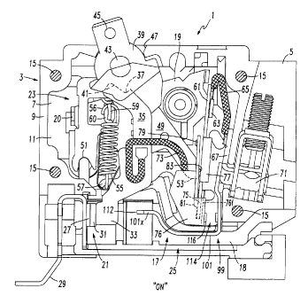
Figure 1 is a side elevation view of a circuit breaker incorporating the
invention with the cover removed and shown in the ON or CLOSED position.
Figure 2 is a view similar to Figure 1 showing the circuit breaker in the
OFF or OPEN position.
Figure 3 is a view similar to Figure 1 showing the circuit breaker in the
TRIPPED position.
Figure 4 is an isometric view of a by-pass conductor which forms part
of the invention.
-4-
CA 02364989 2001-12-14
99-PDC-446
Figure 5 is a section through the circuit breaker taken along the line 5-
in Figure 3.
Figure 6 is an isometric view of a bracket mounting a secondary
contact on the bimetal in accordance with the invention.
5
DESCRIPTION OF THE PREFERRED EMBODIMENTS
Referring to the drawings, the circuit breaker 1 of the invention
comprises an electrically insulating housing 3 having a molded insulating base
5
having a planar wall 7 and edge walls 9 forming a cavity 11. The housing 3
further
includes a molded insulating cover (not shown) which is secured to the base 5
by four
rivets 15. A circuit breaker assembly, indicated generally at 17 in Figure 1,
is
supported in the cavity 11 of the housing. The circuit breaker assembly 17
includes a
support plate 19 having a stop 20, a set of main contacts 21, a latchable
operating
mechanism 23 and trip assembly 25.
The set of main contacts 21 includes a fixed or stationary contact 27
secured to a line terminal 29, and a movable contact 31 secured to the edge of
the free
end 33 of a flat metallic, generally C-shaped contact arm 35 which forms part
of the
latchable operating mechanism 23. The contact arm 35 is provided at the upper
end
with a depression 37. A molded insulating operating member 39 has a molded
part 41
which engages the depression 37 in the contact arm 35 to provide a driving
connection between the operating member 39 and the contact arm 35. The
operating
member 39 is molded with a pair of pins 43 extending outwardly on opposite
sides
(only one shown) which fit into bearing openings (not shown) in the base 5 and
the
cover of the housing 3 to support the operating member 39 for pivoted
movement.
The operating member 39 includes a handle part 45 which extends through an
opening 47 on top of the housing 3 to enable manual operation of the circuit
breaker
1. The operating member 39 also includes downwardly extending portion 48 (see
Figure 2) for engaging the latchable operating mechanism 23 so as to provide
for
resetting the circuit breaker 1 following tripping.
The latchable operating mechanism 23 also includes a cradle 49
supported at one end for pivoted movement on a molded post part 51 of the
insulating
housing base 5. The other end of the cradle 49 has a latch ledge 53 which is
latched
-5-
CA 02364989 2001-12-14
99-PDC-446
by the trip assembly 25, which will be described in more detail herein. An
over center
tension spring 55 is connected, under tension, at one end to a projection 57
near the
lower end of the contact arm 35, and at the upper end thereof to a bent over
projection
59 on the cradle 49.
The trip assembly 25 comprises an elongated bimetal member 61
secured, in proximity to its upper end, to a bent over tab 63 on the support
plate 19. A
flexible conductor 65 is secured at one end to the upper end of the bimetal
member 61
and at the other end to a conductor 67 that extends through an opening in the
housing
3 and is part of a solderless terminal connector 71 that is externally
accessible and
supported in the housing 3 in a conventional manner. Another flexible
conductor or
shunt 73 is secured at one end to the free, lower end 75 of the bimetal member
61
through a bracket 76 described below and at the other end thereof to the
contact arm
35 to electrically connect the contact arm 35 with the bimetal member 61.
The trip assembly 25 includes a thermal trip capability which responds
to persistent low level overcurrents and a magnetic trip capability which
responds
substantially instantaneously to higher overload currents. The trip assembly
25
includes the bimetal member 61, a magnetic yoke 77 and a magnetic armature 79.
The magnetic yoke 77 is a generally U-shaped member secured to the bimetal
member 61 at the bight portion of the magnetic yoke 77 with the legs thereof
facing
the armature 79. The magnetic armature 79 is secured to a supporting spring 81
that
is in turn secured at its lower end near the free end 75 of the cantilevered
bimetal
member 61. Thus, the armature 79 is supported on the bimetal member 61 by the
spring 81. The armature 79 has a window opening 83 through which the one end
of
the cradle 49 extends with the latch ledge 53 on the cradle engaging the edge
of the
window 83 to latch the latchable operating mechanism 23 in the latched
position, as
shown in Figure 1.
With the circuit breaker in the ON position, as shown more particularly
in Figure 1, a persistent overload current of a predetermined value causes the
bimetal
member 61 to become heated and deflect to the right to effect a time delayed
thermal
tripping operation. The armature 79, which is supported on the bimetal member
61 by
means of the leaf spring 81, is carried to the right with the bimetal member
to release
the cradle 49. When the cradle 49 is released, the spring 55 rotates the
cradle
-6-
CA 02364989 2001-12-14
99-PDC-446
clockwise on the post 51 until this motion is arrested by the engagement of
the cradle
with a molded part 85 of the housing base 5. During this movement, the line of
action
of the spring 55 moves to the right of the point at which the contact arm 35
is pivoted
on the operating member 39 to rotate the contact arm counterclockwise to snap
the set
of main contacts 21 open. Figure 3 shows this tripped condition of the circuit
breaker.
The circuit breaker 1 is magnetically tripped automatically and
instantaneously in response to overload currents above a second predetermined
value
higher than the predetermined value for the thermal trip. Flow of overload
current
above this higher predetermined value through the bimetal member 61 induces
magnetic flux around the bimetal. This flux is concentrated by the magnetic
yoke 77
toward the armature 79. Overload current above the second predetermined value
generates a magnetic force of such strength that the armature 79 is attracted
toward
the magnetic yoke 77 resulting in the flexing of the spring 81 permitting the
armature
79 to move to the right to release the cradle 49 and trip the circuit breaker
open in the
same manner as described with regard to thermal tripping operation.
Following either a thermal or a magnetic trip the circuit breaker is reset
by moving the handle 45 to the OFF position and then slightly beyond so that
the
extension 48 on the operating member engages the bent over projection 59 on
the
cradle 49 and rotates the cradle to relatch the latching surface 53 in the
window 83 in
the armature 79. The resulting OFF position is shown in Figure 2. The circuit
breaker 1 may be turned on from this position by rotating the handle
counterclockwise, which through the molded part 41 moves the upper end of the
contact arm to the right in Figure 2. When the contact point 37 on the upper
end of
the contact arm 35 crosses the line of force of the spring 55, the contacts
snap closed
to the ON position shown in Figure 1. The circuit breaker 1 is returned to the
OFF
position manually by moving the handle clockwise as shown in Figure 1.
Referring now to Figures 2 through 4, a bimetal by-pass 99 includes a
bypass conductor 101 shown supported within the housing 3 of the circuit
breaker 1.
The bypass conductor 101 can include an elongated flat strap having a middle
portion
that includes a substantially right-angled body portion 104. The bypass
conductor
101 has a first end 106 adapted to be positioned adjacent to or in contact
with a
contact arm 35 of the circuit breaker 1 in an open circuit position or TRIPPED
-7-
CA 02364989 2001-12-14
99-PDC-446
position of the circuit breaker 1. This permits the bypass conductor 101 to
receive
current, especially high transient current, flowing through the circuit
breaker 1 during
an event such as a circuit overload. A second end 108 of the bypass conductor
101 is
electrically connected to the load terminal 71 of the circuit breaker 1
through the
conductor 67 to provide a path for current between the first end 106 and the
second
end 108 through the bypass conductor 101.
The bypass conductor 101 is preferably composed of a metal such as
copper or another suitable metal alloy or electrically conductive composite.
The
material from which the bypass conductor 101 is composed provides a lower
resistance path relative to the conventional path for electrical current
passing through
the circuit breaker. In the TRIPPED position shown in Figure 3, the contact
arm 35
can come into substantial intimate contact with an end of the bypass conductor
101 or
can be separated, preferably by a bypass gap distance dl of about 0 mm to 0.8
mm
between the end of the bypass conductor 101 and the contact arm 35. By
providing a
relatively lower-resistance path for current in parallel with the conventional
path, the
bypass conductor 101 thereby enables improved interruption of a relatively
high
transient electrical arc. The bypass conductor 101 therefore helps to direct
current
away from the thermal trip mechanism and other components of the circuit
breaker 1.
At least a portion of the bypass conductor 101 is positioned in
communication with a gas vent 18 of the circuit breaker 1. This positioning of
the
bypass conductor 101 in the gas vent 18 promotes commutation of a high
transient
current to the bypass conductor 101.
In operation, when the movable contact portion 31 of the contact arm
35 moves to a substantially full open circuit position, a situation favorable
to arc
formation is provided. Opening of the main contacts 21 in the presence of a
high
transient current produces an arc that can be commutated to the bypass
conductor 101.
This commutation is due primarily to the positioning of the first end 106 of
the bypass
conductor 101 adjacent to or in substantial contact with the flat end 33 of
the contact
arm 35 during movement of the contact arm 35 to open and close the main
contacts
21.
The bypass conductor 101 has an extension 101x on the first end 106
which extends upward and then forward toward the left as viewed in Figures 1,
2 and
-8-
CA 02364989 2001-12-14
99-PDC-446
4 to overlap the flat end 33 of the contact arm 35 with the contact arm in the
open or
tripped positions. The tip 112 of the extension 101 x extends almost to the
moveable
contact 31 which is secured on the end of the flat contact arm. In this
arrangement,
there is an extended area of overlap between the bypass conductor, and the
contact
arm and moveable contact for supporting the secondary arc through which
current is
commutated from the contact arm 35 to the bypass conductor. This commutates
the
current to the bypass conductor soon after the contacts 27 and 31 begin to
open
thereby reducing the energy input to the bimetal and also helps in
interrupting the
main arc between the fixed and moveable contacts 27 and 31.
In order to more completely commutate high transient out of the
bimetal, the bypass conductor 101 is positioned to be electrically connected
to the free
end 75 of the bimetal 61 as the bimetal deflects in response to a very high
overcurrent.
In order to provide an electrical connection with low resistance and good
wear, the
bimetal by-pass 99 further includes a pair of secondary contacts 114 including
contact
116 on the free end 75 of the bimetal 61 and contact 118 on the bypass
conductor 101.
Referring to Figure 6, the secondary contact 116 is secured on a flange 76f of
the
shunt bracket 76 which, as can be seen in Figure 3, also connects the shunt 73
to the
free end of the bimetal 61. This shunt bracket 76 is made of a material with
low
electrical resistance such as copper, and provides a convenient arrangement
for
securing both the shunt 73 and the secondary contact 16 to the limited area
available
on the free end 75 of bimetal 61.
While the bypass conductor could be shortened so that only the vertical
section adjacent the second end 108 and carrying the secondary contact 118 is
provided, it is preferred that the full bypass conductor as described above be
used.
Preferably, the bypass conductor is arranged so that as the magnetic trip
feature
responds to the very high transient current and unlatches the operating
mechanism 23
to open the main contacts 21, some of the current is commutated from the
contact arm
to the end 106 of the bypass conductor 101. This diversion of some of the
current
out of the bimetal slows the deflection of the bimetal, however it continues
to deflect
30 until the secondary contacts 114 close. As the secondary contacts provide a
much
lower resistance path to the load terminal 71 than either the bimetal or the
are between
the contact arm and the extension lOlx on the end 106 of the bypass conductor,
-9-
CA 02364989 2001-12-14
99-PDC-446
virtually all of the current is commutated out of the bimetal 61. This
eliminates the
situation that was observed in some cases of very high overcurrents where even
with
the bypass conductor commutating some of the current from the contact arm to
the
load terminal, the bimetal would be driven against a stop either formed by the
conductor or a molded part of the casing with such force that the bimetal was
permanently deformed, thereby destroying the calibration.
It can therefore be appreciated that the bypass conductor apparatus of
the present invention provides improved protection of sensitive bi-metallic
components within a circuit breaker. The bypass conductor as disclosed
redirects
potentially damaging high transient currents along an alternate, relatively
lower
resistance path through the circuit breaker. The bypass conductor thereby
reduces the
likelihood of damage to the circuit breaker that can be caused by excessive
electrical
current. The bypass conductor can also enhance the useful life and proper
functioning
of the circuit breaker after a transient event has occurred.
While specific embodiments of the invention have been described in
detail, it will be appreciated by those skilled in the art that various
modifications and
alternatives to those details could be developed in light of the overall
teachings of the
disclosure. Accordingly, the particular arrangements disclosed are meant to be
illustrative only and not limiting as to the scope of the invention which is
to be given
the full breadth of the appended claims and any and all equivalents thereof.
-10-