Note: Descriptions are shown in the official language in which they were submitted.
CA 02365004 2001-12-10
MANUFACTURING METHOD FOR A PRINTED WIRING BOARD
Bac ,ground of the Invention:
This invention relates to a method of manufacturing a printed wiring
board used in an electronic apparatus.
Referring to Figs. 1 A through 1 J, description will be made of a method
of manufacturing a printed wiring board as a related art.
Referring to Fig. 1 A, preparation is made of a printed wiring board 1
having a plurality of interlayer connection holes. The printed wiring board 1
comprises an insulator substrate 1 a, a copper plating layer 1 b, and a copper
foil
1 c. The insulator substrate 1 a has through holes formed therein as desired.
Then, the insulator substrate 1 a is subjected to copper plating to form the
copper plating layer 1 b on both surfaces of the insulator substrate 1 a and
inside
surfaces of the through holes. The copper plating layer 1 b formed on the
inside surface of each through hole in the insulator substrate 1 a has an
inner
surtace defining the interlayer connection hole of the printed wiring board 1.
The interlayer connection holes include a large-diameter through hole 2 having
a diameter not smaller than the thickness of the printed wiring board 1 and a
small-diameter through hole 3 having a diameter smaller than the thickness of
the printed wiring board 1. The printed wiring board 1 prepared as mentioned
above is an interlayer connection plating printed wiring board. A hole filling
process is carried out for each single interlayer connection plating printed
wiring
board.
Referring to Fig. 1 B, the printed wiring board 1 is placed on a printing
table 40 in order to carry out the hole filling process using a printing
technique.
CA 02365004 2001-12-10
2
A printing plate or pattern 50 is used to print a hole filling resin (for
example,
epoxy resin) 9. A squeegee 70 serves to apply the hole filling resin 9. After
the printed wiring board 1 is placed on the printing table 40, the printing
pattern
50 is put on the printed wiring board 1 and the hole filling resin 9 is
applied and
spread on the printing pattern 50 covering the printed wiring board 1 by the
use
of the squeegee 70.
Referring to Fig. 1 C, the hole filling resin 9 is applied and spread on the
printing pattern 50 by the squeegee 70. Thus, the hole filling resin 9 is
filled in
the through holes 3 and 2 as filled resins 19 and 20, respectively. After the
through holes 3 and 2 are filled with the hole filling resin 9, the printing
pattern
50 is removed and the printed wiring board 1 is displaced from the printing
table
40.
Referring to Fig. 1 D, the printing pattern 50 is removed from the printed
wiring board 1 and the printed wiring board 1 is displaced from the printing
table
40. In this state, the hole filling resin 9 is cured. In Fig. 1 D, a resin
residue
100 is formed by a part of the hole filling resin 9 which has been present in
an
opening portion of the printing pattern 50 upon filling the hole filling resin
9 in
the through holes 3 and 2 and is left on a surface of the printed wiring board
1
or which leaks from the periphery of the opening portion of the printing
pattern
50. The resin residue 100 also includes a part of the hole filling resin 9
leaking
from a gap between the printing pattern 50 and the printed wiring board 1 in
the
vicinity of open ends of the through holes 3 and 2. The hole filling resin 9
is
cured by heating or photocuring. At this time, both of the filled resins 19
and
20 filled in the through holes 3 and 2 and the resin residue 100 are cured
together. As a result, protrusions are formed on the surface of the printed
wiring board 1. Such protrusions must be removed by polishing or the like.
Referring to Fig. 1 E, the surface of the printed wiring board 1 is
flattened and smoothed by the use of a polisher 110. In order to remove the
CA 02365004 2001-12-10
3
protrusions formed on the surface of the printed wiring board 1 due to
presence
of the resin residue 100 when the hole filling resin 9 is cured and to flatten
and
smooth the surface of the printed wiring board 1, polishing is carried out by
the
use of the polisher 110. At this time, the surface of the printed wiring board
1
is also shaved. As a result of polishing, the printed wiring board 1 as a
whole
is elongated. Since the copper plating layer 1 b and the resin residue 100
different in hardness are simultaneously polished, it is difficult to improve
the
flatness of the printed wiring board 1.
Referring to Fig. 1 F, the protrusions are removed by polishing to
produce flattened surfaces 130 and 120 of the hole filling resin 9 filled in
the
through holes 3 and 2 as the filled resins 19 and 20, respectively. In this
state,
the through holes 3 and 2 may be referred to as filled through holes. Next,
the
printed wiring board 1 with the filled through holes is subjected to plating
(21 in
Fig. 1 G) in the following manner.
Referring to Fig. 1 G, the printed wiring board 1 with the filled through
holes is obtained through the above-mentioned steps and is subjected to
plating
21. By the plating 21, the flattened surfaces 130 and 120 of the filled resins
19
and 20 on both sides of the printed wiring board 1 are provided with plating
layers 22. Thus, on each of the opposite surfaces of the printed wiring board
1,
the copper foil 1 c, the copper plating layer (interlayer connection plating
layer)
1 b, and the plating layer 22 are formed to provide a thick layer. Next, a dry
film
(23 in Fig. 1 H) is adhered onto each surface of the printed wiring board 1
with
the plating layer 22 formed thereon to determine a wiring pattern of the
printed
wiring board 1.
Referring to Fig. 1 H, the dry film 23 having a desired wiring pattern is
adhered to the printed wiring board 1 plated in Fig. 1 G. Thus, the wiring
pattern of the printed wiring board 1 is determined by the dry film 23 having
the
wiring pattern designed for the printed wiring board 1. Next, etching (24 in
Fig.
CA 02365004 2001-12-10
4
1 I) is performed to remove a conductive layer 25 (comprising the plating
layer
22, the copper plating layer 1 b, and the copper foil 1 c) except an area
where
the dry film 23 is attached, as illustrated in Fig. 1 I.
Referring to Fig. 1 I, the printed wiring board 1 with the dry film 23
attached thereto in Fig. 1 H is subjected to the etching 24. The conductive
layer 25 comprises the plating layer 22, the copper plating layer 1 b, and the
copper foil 1 c. After the etching 24, a part of the conductive layer 25 which
is
protected by the dry film 23 is left to form the wiring pattern (connection
pad).
Because the conductive layer 25 is thick, etching accuracy is degraded. Then,
the dry film 23 remaining on the conductive layer 25 is removed as illustrated
in
Fig. 1 J.
Referring to Fig. 1 J, the dry film 23 is removed from the printed wiring
board 1 subjected to the etching 24 in Fig. 1 I to provide the printed wiring
board
1 with the through holes filled and the wiring pattern (connection pad)
determined. In Fig. 1 J, the connection pads are depicted by 34.
Next referring to Figs. 2 and 3, description will be made of a merit
achieved by filling the hole filling resin in the through holes formed in the
printed
wiring board 1 as illustrated in Figs. 1A through 1J.
Referring to Fig. 2, a component 32 is mounted on the printed wiring
board 1 in which the through holes are not filled. Referring to Fig. 3, the
component 32 is mounted on the printed wiring board 1 in which the through
holes are filled.
In Fig. 2, the hole filling resin 9 is not filled in the through hole 3 as the
filled resin 19. Therefore, a connection pad to connect the component 32 can
not be formed on the through hole 3. On the other hand, in Fig. 3, the through
hole 3 is filled with the hole filling resin 9 as the filled resin 19.
Therefore, a
connection pad 34 comprising the copper plating layer 22 can be formed on the
filled resin 19 filled in the through hole 3 in such a manner that the
connection
CA 02365004 2001-12-10
pad 34 is connected to the copper plating layer 1 b of the printed wiring
board 1.
Then, the component 32 can be mounted on the connection pad 34 located on
the through hole 3.
As illustrated in Fig. 3, the connection pad 34 is formed on the through
hole 3 with the filled resin 19 buried therein and the component 32 is
directly
connected to the connection pad 34 located on the through hole 3. In this
manner, the wiring distance is shortened and the inductance is reduced as
compared with Fig. 2. Thus, the impedance of the printed wiring board 1 is
reduced.
As illustrated in Fig. 3, the filled resin 19 is buried in ~e through hole 3
so that the connection pad 34 can be formed on the through hole 3 and the
component 32 can be directly connected to the connection pad 34 on the
through hole 3. Thus, as compared with Fig. 2, the wiring distance is
shortened and the inductance is reduced so that the impedance of the printed
wiring board 1 is reduced. In this method, however, the complicated steps
described in conjunction with Figs. 1A through 1 F are required in order to
fill the
through hole 3 with the filling resin 9 as the filled resin 19. This decreases
the
efficiency in production. As illustrated in Figs. 1 A through 1 G, a metal
layer on
the surface of the printed wiring board 1 comprises the copper foil, the
interlayer
connection plating layer, and the pad. Therefore, the metal layer is thick so
that patterning accuracy is inferior.
Furthermore, in the method described in conjunction with Figs. 1 A
through 1 J, the hole filling process must be followed by polishing as
described
in conjunction with Figs. 1 E and 1 F. Therefore, the productivity is inferior
and
the printed wiring board 1 is heavily damaged..
~~u_mmarv of the Invention:
It is an object of this invention to provide a method of manufacturing a
printed wiring board, which is capable of forming a connection pad on a
through
CA 02365004 2001-12-10
6
hole without carrying out a hole filling process for the through hole.
It is another object of this invention to provide a printed wiring board in
which a connection pad can be formed on a through hole without carrying out a
hole filling process for the through hole.
According to this invention, there is provided a method of manufacturing
a printed wiring board (81 ), comprising the steps of:
preparing an insulator substrate (1 a) having first and second principal
surfaces opposite to each other;
forming a first metal foil (82) on the first principal surface;
temporarily fixing a thermosetting resin film (84) to the second principal
surface with the thermosetting resin film brought into contact with the second
principal surface;
drilling, with the thermosetting resin film temporarily fixed to the second
principal surface, a through hole (86) simultaneously in the first metal foil,
the
insulator substrate, and the thermosetting resin film so that the through hole
extends in a direction substantially perpendicular to the first and the second
principal surfaces;
simultaneously heating and vacuum-pressing, with a second metal foil
(87) brought into contact with the thermosetting resin film after the drilling
step,
the first metal foil, the insulator substrate, the thermosetting resin film,
and the
second metal foil to obtain an intermediate printed wiring board in which a
bottom (92) of the through hole is covered with the second metal foil and in
which the bottom of the through hole has a corner provided with a corner
rounded portion (93) formed by the thermosetting resin film so as to protrude
from the corner; and
forming a metal plating layer (95) on the first and the second metal foils
of both sides of the intermediate printed wiring board, on an inner wall of
the
through hole, on the corner rounded portion, and on an exposed surface of the
CA 02365004 2001-12-10
7
second metal foil exposed through the bottom of the through hole to obtain a
final printed wiring board provided with interlayer connection.
According to this invention, there is also provided an interlayer
connection printed wiring board (81 ) obtained by the steps of:
preparing an insulator substrate (1 a) having first and second principal
surfaces opposite to each other;
forming a first metal foil (82) on the first principal surface;
temporarily fixing a thermosetting resin film (84) to the second principal
surface with the thermosetting resin film brought into contact with the second
principal surface;
drilling, with the thermosetting resin film temporarily fixed to the second
principal surface, a through hole (86) simultaneously in the first metal foil,
the
insulator substrate, and the thermosetting resin film so that the through hole
extends in a direction substantially perpendicular to the first and the second
principal surfaces;
simultaneously heating and vacuum-pressing, with a second metal foil
(87) brought into contact with the thermosetting resin film after the drilling
step,
the first metal foil, the insulator substrate, the thermosetting resin film,
and the
second metal foil to obtain an intermediate printed wiring board in which a
bottom (92) of the through hole is covered with the second metal foil and in
which the bottom of the through hole has a corner provided with a corner
rounded portion formed by the thermosetting resin film so as to protrude from
the corner; and
forming a metal plating layer (95) on the first and the second metal foils
of both sides of the intermediate printed wiring board, on an inner wall of
the
through hole, on the corner rounded portion, and on an exposed surface of the
second metal foil exposed through the bottom of the through hole.
CA 02365004 2001-12-10
a
According to this invention, there is also provided a printed wiring board
(81 ) including:
an insulator substrate (1 a) having a first principal surface and a second
principal surface opposite to the first principal surface; and
a first metal layer (87) formed on the second principal surface;
the insulator substrate having a through hole (86) which is formed
therein and extends in a direction substantially perpendicular to the first
and the
second principal surfaces so that a part of a surface of the first metal layer
is
exposed as an exposed surface through a bottom (92) of the through hole;
the printed wiring board comprising a second metal layer (95) formed
on the first principal surface of the insulator substrate, on an inner wall of
the
through hole, and on the exposed surface of the first metal layer.
Figs. 1 A through 1 J are views for describing a method of manufacturing
a printed wiring board according to a related art;
Fig. 2 is a perspective view of a printed wiring board with an interlayer
connection hole (through hole) left unfilled and a component mounted thereon;
Fig. 3 is a perspective view of the printed wiring board in Fig. 1 J after an
interlayer connection hole (through hole) is filled and a component mounted
thereon; and
Figs. 4A through 4J are views for describing a method of manufacturing
a printed wiring board according to an embodiment of this invention; and
Fig. 5 is a perspective view showing the printed wiring board in Fig. 4J
and a component mounted thereon.
Now, this invention will be described with reference to the drawing.
Referring to Figs. 4A through 4J, description will be made of a method
of manufacturing a printed wiring board according to an embodiment of this
CA 02365004 2001-12-10
9
invention.
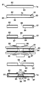
At first referring to Fig. 4A, the printed wiring board 81 comprises an
insulator substrate 1 a and a copper foil 82 formed on one surface of the
insulator substrate 1 a. The insulator substrate 1 a has the other surface as
a
substrate resin surface 83 where a resin is exposed. As will be described in
the following, a thermosetting resin film (84 in Fig. 4B) is put on the
substrate
resin surface 83 of the printed wiring board 81 and temporarily or
preparatorily
fixed.
Referring to Fig. 4B, the thermosetting resin film 84 is temporarily fixed
to the printed wiring board 81 at temporary fixing portions 85. The
thermosetting resin film 84 is low in resin flowability. As illustrated in
Fig. 4B,
The thermosetting resin film 84 is placed at a base. The printed wiring board
81 is put on the thermosetting resin film 84 so that the substrate resin
surface
83 is faced to the thermosetting resin film 84. Next, the temporal fixing
portions 85 of the thermosetting resin film 84 are heated or otherwise treated
to
melt and then solidify the thermosetting resin film 84. As a consequence, the
substrate resin surface 83 and the thermosetting resin film 84 are adhered and
temporarily fixed. The temporal fixing portions 85 may be located at any
desired positions where no wiring or no through hole is present on the printed
wiring board 81. At this stage, the thermosetting resin film 84 is unchanged
in
its state except the temporal fixing portions 85. In other words, the
thermosetting resin film 84 has no adhesive effect in an area except the
temporal fixing portions 85. Next, a through hole (86 in Fig. 4C) is formed in
the printed wiring board 81 and the thermosetting resin film 84 integrally
coupled therewith in the following manner.
Referring to Fig. 4C, the through hole 86 is formed in the printed wiring
board 81 and the thermosetting resin film 84 temporarily fixed thereto. As
illustrated in Fig. 4C, the through hole 86 is formed by drilling in the
printed
CA 02365004 2001-12-10
l
wiring board 81 and the thermosetting resin film 84 integrally coupled with
each
other at the temporal fixing portions 85 in Fig. 4B. As a consequence, through
holes equal in diameter and coincident in position are formed in the printed
wiring board 81 and the thermosetting resin film 84 to define the through hole
86 of the printed wiring board 81. Next, as illustrated in Fig. 4D, the
printed
wiring board 81 and the thermosetting resin film 84 with the through hole 86
formed therein are put on a metal foil 87 and assembled together.
Referring to Fig. 4D, the printed wiring board 81 and the thermosetting
resin film 84 with the through hole 86 formed therein as an interlayer
connection
hole in Fig. 4C are assembled on the metal foil 87 to be subjected to vacuum
pressing and heating. As illustrated in Fig. 4D, the metal foil 87, the
thermosetting resin film 84, and the printed wiring board 81 are stacked in
this
order from the bottom. At this stage, the printed wiring board 81 and the
thermosetting resin film 84 are temporarily fixed. In the above-mentioned
assembling, the printed wiring board 81 with the thermosetting resin film 84
are
simply stacked on the metal foil 87 without using any substance having an
adhesive effect. Next, a resultant assembly is put into a press to be
subjected
to vacuum pressing (88 in Fig. 4E) and heating so that the metal foil 87 is
adhered.
Referring to Fig. 4E, the assembly in Fig. 4D is subjected to the vacuum
pressing 88 and the heating. The printed wiring board 81, the thermosetting
resin film 84, and the metal foil 87 assembled into a pressable state in Fig.
4D
are put into the press to be subjected to the vacuum pressing 88 and the
heating. By the heating, the thermosetting resin film 84 is melted so that the
substrate resin surface 83 of the printed wiring board 81 is brought into
tight
contact with the metal foil 87. In the figure, a reference numeral 89
represents
a bottom of the through hole 86 formed in the thermosetting resin film 84 and
in
the printed wiring board 81 to be coincident in position and equal in
diameter.
CA 02365004 2001-12-10
Z1
The metal foil 87 is exposed at the bottom 89. A reference numeral 90
represents a bottom surrounding portion of the through hole 86. The
thermosetting resin film 84 melted by the vacuum pressing slightly leaks to
the
bottom surrounding portion 90. The thermosetting resin film 84 leaking as
mentioned above is poor in resin flowabiiity and therefore stays in the bottom
surrounding portion 90 to form a corner rounded portion or a corner R portion
(93 in Fig. 4F) without spreading out of the bottom surrounding portion 90. By
the heating, the thermosetting resin film 84 adheres the printed wiring board
81
and the metal foil 87 and is solidified. At the bottom surrounding portion 90
of
the through hole 86, the thermosetting resin film 84 is solidified to form the
corner rounded portion (or the corner rounded portion). Next, the printed
wiring board 81, the thermosetting resin film 84, and the metal foil 87
integrally
coupled with one another by the vacuum pressing and the heating are removed
from the press.
Referring to Fig. 4F, the printed wiring board 81 kept in tight contact with
the metal foil 87 by the vacuum pressing and the heating in Fig. 4E are
removed from the press. The metal foil 87 is exposed at a bottom 92 of the
through hole 86. The corner rounded portion (or the corner R portion) 93, is
formed by solidification of the thermosetting resin film 84 at the bottom
surrounding portion 90 of the through hole 86. The metal foil 87 has an outer
surface (a lower surface in the figure) which is flat without irregularities.
The printed wiring board 81 in the state illustrated in Fig. 4F will be
referred to as an intermediate printed wiring board.
Next, the intermediate printed wiring board illustrated in Fig. 4F is
subjected to plating (94 in Fig. 4G) to provide interlayer connection.
Referring to Fig. 4G, the printed wiring board 81 removed from the
press with the metal foil 87 attached thereto as illustrated in Fig. 4F is
subjected
to the plating (for example, copper plating) 94 to provide interlayer
connection.
CA 02365004 2001-12-10
is
When the printed wiring board 81 with the metal foil 87 adhered thereto is
subjected to the plating 94, the copper foil 82 and the metal foil 87 on the
printed wiring board 81 are plated. In the through hole 86, circulation of a
plating solution is improved by the shape of the corner rounded portion (or
the
corner R portion) 93 so that a plating layer 95 is formed on an upper surface
of
the metal foil 87 at the bottom 92 of the through hole 86, on a wall surface
91 of
the through hole 86, and on the corner rounded portion (or the corner R
portion)
93 of the through hole 86 to thereby complete the interlayer connection.
The printed wiring board 81 in the state where the interlayer connection
is completed as illustrated in Fig. 4G will be referred to as a final printed
wiring
board. The printed wiring board 81 in the state where the interlayer
connection
is completed as illustrated in Fig. 4G may also be referred to as a closed-
hole
printed wiring board because the bottom of the interlayer connection hole is
closed by the metal.
Referring to Fig. 4G, the printed wiring board 81 in the state where the
interlayer connection is-completed has a following structure. Specifically,
the
printed wiring board 81 includes an insulator substrate 1 a having a first
principal
surface and a second principal surface opposite to the first principal surface
and
a first metal layer (87, 95) formed on the second principal surface. The
insulator substrate 1 a has a through hole 86 which is formed therein and
extends in a direction substantially perpendicular to the first and the second
principal surfaces so that a part of a surface of the first metal layer (87,
95) is
exposed as a exposed surface through a bottom of the through hole 86. The
printed wiring board 81 further includes a second metal layer (95) formed on
the
first principal surface of the insulator substrate 1 a, on an inner wall of
the
through hole 86, and on the exposed surface of the first metal layer 87. In
the
illustrated example, a combination of the copper foil 82 and the plating layer
95
is formed on the first principal surface of the insulator substrate 1 a as the
CA 02365004 2001-12-10
13
second metal layer.
Next, a dry film (97 in Fig. 4H) having a desired wiring pattern is
adhered to the interlayer connection printed wiring board (closed-hole printed
wiring board) to determine the wiring pattern of the printed wiring board 81.
Referring to Fig. 4H, the dry film 97 is adhered to the printed wiring
board 81 provided with the interlayer connection in Fig 4G. The printed wiring
board 81 provided with the interlayer connection in the above-mentioned steps
is the closed-hole printed wiring board 96. In the closed-hole printed wiring
board 96, one side of the through hole 86 as the interlayer connection hole is
covered with the metal foil 87 and the plating layer 95 and is flat without
irregularities. The dry film 97 has the desired printed pattern. The dry film
97
is adhered to the closed-hole printed wiring board 96 to determine the wiring
pattern. Then, etching (98 in Fig. 41) is carried out to form the wiring
pattern of
the closed-hole printed wiring board 96.
Referring to Fig. 41, the closed-hole printed wiring board 96 with the dry
film 97 attached thereto in Fig. 4H is subjected to the etching 98. By the
etching 98, the metal foil 82, the metal foil 87, and the plating layer 95 are
removed except those portions protected by the dry film 97 to form the wiring
pattern of the closed-hole printed wiring board 96. Next, the dry film 97 is
detached.
Referring to Fig. 4J, the dry film 97 is detached from the closed-hole
printed wiring board 96 subjected to the etching in Fig. 4H. In the closed-
hole
printed wiring board 96 illustrated in the figure, the dry film 97 is detached
and
the wiring pattern (connection pad) is completed. In Fig. 4J, the connection
pad 34 comprises the metal foil 87 and the plating layer 95.
Referring to Fig. 5, a component 32 is mounted on the closed-hole
printed wiring board 96 according to this invention. The component 32 is
directly connected to the connection pad 34 formed on the through hole 86.
CA 02365004 2001-12-10
14
Therefore, as compared the case where the through hole is not filled as
illustrated in Fig. 2, the wiring distance is shortened and the inductance is
reduced. Thus, like in the case where the printed wiring board with the
through
hole filled by the printing technique is used as illustrated in Fig. 3, the
impedance of the printed wiring board 81 is reduced.
In the printed wiring board with the through hole filled by the printing
technique as illustrated in Fig. 3, the connection pad 34 is formed on the
filled
resin 19 buried in the through hole. Therefore, mountability of the component
32 depends on the smoothness of the surface of the filled resin 19. On the
other hand, in the closed-hole printed wiring board 96 according to this
invention, the connection pad 34 in Fig. 5 is obtained by forming the plating
Layer 95 on the metal foil 87 as illustrated in Fig. 4J. Therefore, no
polishing
step is required and the smoothness is excellent. The mountability of the
component is good and stable.
In this invention, one end (bottom) of the through hole 86 is covered
with the metal foil 87 as illustrated in Fig. 4F. Furthermore, the corner
rounded
portion (or the corner R portion) 93 is formed around the bottom of the
through
hole 86. Therefore, the plating 94 illustrated in Fig. 4G is improved in
coating
characteristics to increase the thickness of the plating layer 95 in the
through
hole 86. Furthermore, by the plating, hole filling by the metal is possible so
that the electric resistance can be minimized. As illustrated in Fig. 5, the
bottom of the through hole 86 is covered with the metal foil 87 in Fig. 4J.
Therefore, no land is required at the pad 34.
As described above, according to this invention, it is possible to
manufacture the printed wiring board in which the connection pad can be
formed on the through hole without carrying out the hole filling process for
the
through hole. Thus, the efficiency in production can be improved.