Note: Descriptions are shown in the official language in which they were submitted.
CA 02365486 2001-12-18
00-EDP-243 1
APPARATUS AND METHOD FOR PROTECTING A LOAD
FROM FLUCTUATIONS IN SUPPLY VOLTAGE
BACKGROUND OF THE INVENTION
Field of the Invention
This invention relates to load monitoring through the use of a switch
which disconnects the load from the source when the voltage is outside
selected limits
and turns the switch back on when the voltage returns to within the selected
limits. In
particular, it relates to eliminating chatter of the switch when the voltage
fluctuates
around the selected limits by introducing adaptive hysteresis into control of
the switch
and also to a simple rapid apparatus and method for detecting phase loss.
Background Information
Various types of voltage monitoring apparatus are known that
disconnect a load if the supply voltage deviates from preset limits. The load
is
reconnected when the voltage is again within the limits. A problem associated
with
this disconnecting and reconnecting high current loads is that the voltage
level can
fluctuate within a few cycles about the trip settings causing the load to be
turned off
and on in rapid succession. The introduction of hysteresis into the control
circuit of
the switch connecting and disconnecting the load can prevent the rapid
oscillation or
instability when the voltage level is close to the set limits. Typically, this
hysteresis is
provided by the introduction of feedback to the input of an analog comparator
from
the comparator output or by use of a time delay circuit. Both of these
approaches
introduce a fixed hysteresis into the control circuit and will not
automatically
accommodate for various levels of voltage fluctuation. Sufficient hysteresis
can be
introduced into the control circuit to reduce the susceptibility of the
monitor to
voltage fluctuations; however, the accuracy of the monitor is degraded.
Another problem for voltage monitoring is the increased generation of
harmonics in power circuits resulting in great part from the widespread
utilization of
power switching semiconductor devices. Most of the present day voltage
monitoring
CA 02365486 2001-12-18
00-EDP-243 2
devices monitor the peak or average voltage. While the damaging heating
effects of
an ac waveform represented by the RMS value can readily be determined from the
peak value for a pure sinusoidal waveform, harmonics cause the ac waveform to
distort. One effect is the flattening of the top of the waveform. In such a
case, the
RMS value of the waveform is not readily determinable from the peak value.
Peak
detecting and average voltage monitoring circuits that are calibrated for
sinusoidal
waveforms will not turn off the power to the load if the peak voltage limit is
not
reached. However, the RMS value of the voltage waveform can be above the
rating
of the load and cause damage.
Another common function of voltage monitors is detection of loss of a
phase. When an overvoltage occurs in a three-phase system, one phase might be
shorted to ground. Typical approaches to loss of phase detection employ
calculation
and can require a half cycle.
There is a need, therefore, for improved apparatus and method for
protecting loads from fluctuating ac supply voltages.
SUMMARY OF THE INVENTION
This need and others are satisfied by the invention which is directed to
apparatus for protecting a load from fluctuations in ac supply voltage by
utilization of
adaptive hysteresis to eliminate chattering of an electrically controlled
switch which
disconnects the load when the supply voltage is outside of selected limits and
reconnects the load by closing the switch when the voltage returns to within
the
limits. In particular, the apparatus comprises an electrically controlled
switch
connecting a load to the ac source, a voltage monitor monitoring the voltage
applied
to the load, and a controller. The controller includes means turning the
switch off
when the voltage applied to the load is outside selected limits and turns the
switch
back on when the voltage returns to within the selected limits. The controller
further
includes adjusting means detecting chattering of the switch and progressively
adjusting the selected limits from preselected base limit values until the
chattering is
eliminated. By chattering, it is meant that the switch turns off and on
rapidly.
Chattering can be measured by the number of times that the switch is turned
off and
CA 02365486 2001-12-18
00-EDP-243 3
back on within a predetermined time interval. The adjusting means can include
means incrementally progressively adjusting the selected limits until this
chattering of
the switch is eliminated. The adjusting means further includes reset means
resetting
the selected limits to the preselected base limits upon the occurrence of a
predetermined condition, which in the exemplary embodiment of the invention is
the
absence of chattering for a predetermined time period.
The voltage monitor digitizes the supply voltage and utilizes samples
of the voltage generated over one quarter cycle. Preferably, the samples taken
over
one quarter cycle are used to generate an RMS value for the voltage. This
rapid
determination of the RMS voltage using samples gathered over one quarter cycle
is
particular advantageous in a three-phase ac system where the RMS voltage in
the
three phases is generated from samples taken in successive quarter cycles of
the three
phases.
The invention also embraces apparatus for rapidly detecting a phase
loss. Apparatus converts the ac waveform to a square wave and then detects the
leading edge of the square wave. Absence of the leading edge indicates a phase
loss.
This apparatus can include means which looks for a square wave to reach a
predetermined amplitude within a designated time interval after a zero
crossing.
The invention also embraces a method of protecting a load from
fluctuations in supply voltage applied to the load through an electronic
switch by
monitoring the ac voltage, turning the switch off when the voltage exceeds
selected
limits and turning the switch back on when the voltage returns within the
selected
limits, detecting chattering of the switch and progressively adjusting the
selected
limits from preselected base limit values until the chattering is eliminated.
The limits
can be progressively adjusted by incrementally adjusting the selected limits
until the
chattering ceases. Also, the chattering can be detected by counting the number
of
times the switch is turned off and then on within a selected time interval.
The
monitoring of the voltage can be effected by use of digital samples over one
quarter
cycle, and for a multiphase system using samples taken in one quarter cycles
of each
phase. The method also includes monitoring the voltage in a multiphase system
for
phase loss by generating a square wave from the ac voltage and checking for
the
CA 02365486 2001-12-18
00-EDP-243 4
leading edge of the square wave. The leading edge of the square wave can be
detected by checking for a predetermined amplitude of the square wave within a
designated period of time after a projected zero crossing.
BRIEF DESCRIPTION OF THE DRAWINGS
A full understanding of the invention can be gained from the following
description of the preferred embodiments when read in conjunction with the
accompanying drawings in which:
Figure 1 is a block diagram of an electrical system incorporating the
invention.
Figure 2 is a schematic diagram of the system of Figure 1.
Figure 3 is a flow chart for a program which determines the RMS
voltage in accordance with the invention.
Figures 4a and 4b taken together illustrate a flow chart of a program
for eliminating chatter of the switches in the system described in Figure 1.
Figure 5 is a timing diagram illustrating the operation of the program
of Figures 4a and 4b.
DESCRIPTION OF THE PREFERRED EMBODIMENTS
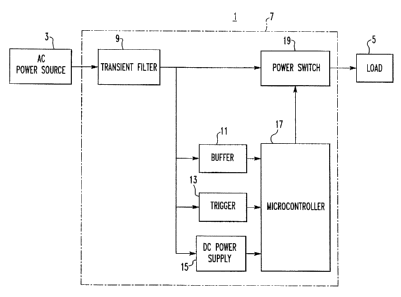
Figure 1 illustrates an ac electric power system 1 in which an ac power
source 3 provides power to a load 5. Apparatus in the form of a voltage
monitor 7
protects the load 5 from fluctuations in the voltage provided by the ac source
3. The
line voltage monitor 7 has six major components: a transient filter 9, a
buffer 11, a
trigger 13, a do power supply 15, a microcontroller 17, and a power switch 19.
The
exemplary ac power system 1 is three phase; however, it is shown in single
line form
in Figure 1 for clarity.
The transient filter 9 is a low pass filter which protects the load 5 and
the input circuitry of the line voltage monitor from rapidly rising voltage
transients.
The buffer 11 provides matching of the input impedance of the microcontroller
17
with that of the input supply voltage, which as will be seen, is reduced by
voltage
dividers. The do power supply 15 provides power for the microcontroller 17 and
its
associated circuits. The trigger 13 initiates sampling of the ac voltages, and
also
CA 02365486 2001-12-18
00-EDP-243 5
provides a signal when there is a phase loss. The power switch 19 connects and
disconnects the load 5 from the ac source 3 under the control of the
microcontroller
17.
The microcontroller 17 digitizes samples of the analog voltages. The
digital samples are taken over a quarter cycle for processing by the
microcontroller to
generate an RMS value of each voltage. When the RMS voltage exceeds selected
limits, that is goes above a selected high limit or below a selected low
limit, the
microcontroller 17 turns the power switch 19 off, which in turn turns off the
power to
the load 5. When the power is again within the limits, the microcontroller
turns the
power switch 19 back on.
Should the ac voltage fluctuate, causing the power switch 19 to chatter,
that is to rapidly turn off and on, the microcontroller progressively adjusts
the limits
by narrowing them through lowering the upper limit and raising the lower limit
until
the chattering is eliminated. This is accomplished by the microcontroller 17
by
progressively incrementally adjusting the selected limits until the chattering
terminates. The chattering is detected by counting the number of times that
the power
switch 19 is turned off and back on within a selected time interval. In the
exemplary
embodiment of the invention, turning off and back on of the switch twice
within the
time period that it takes fox the switch to mechanically turn off twice and
turn on
twice, together with the times required to gather the samples to make the
voltage
measurements (the acquisition time) and the time for the microcontroller to
process
the sample (the processing time). Collectively, the acquisition time plus the
processing time may be referred to as the detection time. As will be seen,
each time
the power switch 19 chatters, a count is incremented. The cumulative value of
this
count is used to adjust the selected limits from a preselected base limit
value. Thus,
when chattering is detected; the limits of the voltage monitor are narrowed.
If
chattering is not eliminated, the count is incremented and the selected limits
are
further narrowed. This process continues until the chattering is eliminated.
Under
predetermined conditions, in the exemplary embodiment when chattering has been
eliminated for a predetermined period of time, the microcontroller resets the
selected
limits back to the preselected base limits. Hence, it can be seen that the
selected
CA 02365486 2001-12-18
00-EDP-243 6
limits for the voltage are progressively, incrementally adjusted until
chattering is
eliminated. Therefore, only the amount of hysteresis required to prevent
chattering is
introduced and therefore, accuracy is preserved as much as possible.
Figure 2 is a detailed schematic diagram of the line voltage monitor 7
for protecting a three-phase load 5 from fluctuations in the three-phase
supply voltage
provided on the phase lines 3A-3C having a nominal voltage of 380 VAC line to
line.
It should be noted that the invention could be applied to single phase
applications by
simply reducing the number of channels.
The transient filter 9 includes metal oxide varistors (MOV) 21 which
clamp voltage transients between the phase lines 3A-3C. The voltage ratings of
these
MOVs 21 are such that they clamp above the highest expected voltage between
the
lines 3A-3C. This prevents the MOVs 21 from turning on when there is a long
duration of overvoltage, e.g., more than one half cycle. During this
condition, the
microcontroller 17 turns off relays 19A-19C which form the power switch 19,
thereby
preventing the load 5 from seeing the overvoltage condition.
Additional MOVs 23 provide common mode transient protection.
Three phase coil 25 and capacitors 27 form a low pass filter 29, which filters
high
frequency transients. The low pass filter 29 also attenuates high frequency
signals
greater than one half the sampling rate of the microcontroller 17, thereby
operating as
an anti-abasing filter.
MOVs 31 provide secondary protection by clamping any voltage
transient remnants. The transient filter 9 protects both the load 5 and the
remainder of
the line voltage monitor 7 from high frequency voltage disturbances, i.e.,
noise, on the
phase lines 3A-3C. The filtered voltage output from the transient filter 9 is
supplied
on the leads 33A-33C to the buffer 1 l, trigger 13, and the do power supply
15. This
do power supply 15 includes an input transformer 35 which is connected to the
lead
33B and 33C. The transformer 59 feeds a bridge rectifier 37, which in
conjunction
with a capacitor 39 and voltage regulator 41, provides regulated do power on
lead 43.
A zener diode 45 connected across the bridge 37 prevents the voltage from
exceeding
the rated input voltage of the regulator 41.
CA 02365486 2001-12-18
00-EDP-243 7
The buffer 11 includes for each phase a voltage divider formed by the
resistors 45, 47 and 49 that reduce the voltages from the lines 33A-33C to a
level that
can be processed by the microcontroller 17. Capacitors 53 and back-to-back
zener
diodes 55 protect the inputs of op amps 57 in the buffers and op amps 59 in
the trigger
13 from voltage transients coming from the load 5. The zener diodes 55 also
limit the
voltage input level to five volts, which is the maximum input of
microcontroller 17.
The op amps 57 and 59 are LM224 or the like. Diodes 61 provide a path to
ground
during the negative voltage excursions of the lines 33A-33C. Therefore, only
positive
voltages are seen by the inputs of the op amps 57 and 59. If the diodes 61
were
removed, a -VDC supply with the same values as the positive supply would be
required. The diodes 61 simplify the power supply circuit. The diodes 61 are
Schottky type 1N5817 which provide a low forward voltage drop. The voltage
dividers formed by the network of resistors 45, 47 and 49 are scaled to the
maximum
range of the microcontroller 17, which in this case is 5 VDC. Due to the large
values
of the resistors 45, current flowing to the diodes 61 is negligible, and
consequently, so
is the offset voltage produced thereby. Also, using the maximum scale of
microcontroller 17 reduces the effect of the offset voltage.
Op amps 57 are configured in a buffer or voltage follower
configuration to match the high impedance of the voltage dividers with the low
input
impedance of the microcontroller 17. Resistors 63 provide a minimal load to
the op
amps 57. Microcontroller 17 samples each phase voltage sequentially, and
during this
time, only one phase is being measured and connected to the input of the
microcontroller 17.
The op amps 59 of the trigger 13 generate square wave outputs on the
positive half cycles of the ac voltage waveforms from the lines 33B-33C. The
microcontroller 17 starts sampling when a positive pulse is detected from the
output
of an op amp 59. Resistors 67 provide minimum loads to the output of the op
amps
59. Capacitors 69 filter noise from the op amps 59. The square waves generated
by
the trigger are used also in loss of phase detection.
Microcontroller 17 is an 8 bit microchip PIC16C715 with a built in
four channel ADC (analog to digital converter). The internal ADC voltage
reference
CA 02365486 2001-12-18
00-EDP-2.43 8
is the do supply voltage provided on the lead 43. It should be noted that a
separate
ADC and voltage reference could be used. Capacitor 71 acts as a decoupling
capacitor. Resistor 73 is necessary for resetting the microcontroller 17
during power-
up.
Microcontroller 17 takes 67 samples in a quarter cycle and performs an
RMS computation. The RMS value of the voltage is then compared to a selected
limit. When this voltage is outside the selected limits, the microcontroller
17 sends a
trip signal to FET 75 through resistor 77: The FET 75 drain lead is connected
directly
to the negative coil terminals of the relays 19A-19C. Light emitting diode
(LED) 79
serves as a simple trip visual indicator. It is on when the relays 19A-19C are
off.
Resistor 81 limits current flowing to the LED 79. Diode 83 protects the FET 75
from
overvoltage when the relays 19A-19C are turned off.
Figure 3 illustrates the flowchart 85 implemented by the
microcontroller 17 to calculate the RMS voltages. Initially during power-up,
microcontroller 17 checks the phase sequence and determines which op amp 59 to
check first. For example, if line 33A starts the phase sequence, then the
microcontroller 17 checks first the op amp 59 connected to that line: Each
time the
program 85 is called for each phase, a check is made for phase loss. Thus, the
output
of the appropriate op amp 59 in the trigger 13 is checked at 87 and a timer is
started at
89. As discussed, the microcontroller 17 checks for phase loss by looking for
the
leading edge of the square wave generated by the appropriate op amp 59. This
is
detected by determining whether output of the op amp has reached a preselected
amplitude as determined at 91 within a predetermined time period, such as 1
ms, as
determined at 93. If this does not occur, indicating a loss of that phase, all
of the
relays 19a-19c are turned off at 95 and the timer is reset at 97.
Assuming that the phase voltage is present, a loop is entered at 99 to
gather and process the digitized samples j of the voltage generated by the
ADC. In
order to generate an RMS value of the voltage, the sample is multiplied by
itself and
then by 2 at 101 and added to an accumulator in 103. When the selected number
of
samples N have been processed as determined at 105, the accumulated value is
divided by 2N at 107. The square root is then taken at 109 to generate the RMS
value
CA 02365486 2001-12-18
00-EDP-243 9
at 111. As the half cycles of voltage are symmetrical at the 90° point,
or one quarter
cycle, the voltage can be sampled for one quarter cycle with each sample value
doubled. {Actually it is not necessary to double the samples as the factor of
2 is
cancelled out when the accumulated value is divided by 2 times the number of
samples at 107).
The number of equally spaced samples that can be taken in a quarter
cycle depends upon the operating frequency of the microcontroller 17. In the
exemplary system, the internal operating frequency of the microcontroller 17
was
selected as 5 MHz. This permits sampling and calculation of the RMS value for
sixty-seven samples in a total time of 4.25 ms. An advantage of quarter cycle
sampling for a three phase system is that the phases may be successively
immediately
sampled in rotation for a sixty cycle wave form. As one cycle in a 60 Hz
system is
16.6 ms, and the phases are 120° apart, there is 5.55 ms between the
phases which is
substantially less than the 4.25 ms required to calculate the RMS voltage
value.
Once each cycle, the program 113 illustrated in Figures 4a and 4b is
run. This controller program 113 controls the turning on and off of the power
switch
19, including adjustment of the limits for a turn on and turn off which
provide the
adaptive hysteresis for the voltage monitor. This program utilizes two timers:
an off
timer which records the time since the power switch was turned off, and an on
timer
which times the time since the power switches were turned on. It also includes
an ON
counter which counts the number of times that the power switch has been turned
on
and a separate count which is the number of times that the power switch has
been
turned off and on twice within a selected time interval. This latter count is
count of
the chattering of the power switch.
The controller program 113 starts off by temporarily storing the RMS
value of voltage at 115. The program 113 is run for each phase. If the count
of the
number of times that the power switch has been turned from ON to OFF twice
within
the selected time period is 0 at 117, i.e., no chattering has been detected,
then the
registers for the selected voltage limits are set to the preselected base
values at 119.
Otherwise, the selected limits are adjusted at 121 by subtracting the count
for the high
or positive limit and adding the count for the low or negative limit. If the
measured
CA 02365486 2001-12-18
00-EDP-243 10
voltage is above the high limit at 123 or below the low limit at 125, i.e.,
outside of the
selected limits, the power switch is turned off at 127. If the flag is 0 at
129, indicating
that the power switch was previously on and has just been turned off, the on
timer is
stopped at 131 and the off timer is started at 133. The off timer is then
checked at 135
and if it is timed out, it is reset at 137. The off timer is checked at 135
also on
subsequent runs of the routine where the switch has remained off and hence the
flag is
equal to 1 at 129. The off time limit is equal to the mechanical delay time
for the
switch to turn off plus the acquisition time to generate the RMS value of the
voltage
and plus the processing time for the microcomputer to run the program 113.
Next, the
flag is set to 1 at 139 if it was previously at 0.
If the RMS value of the voltage is between the limits as determined at
123 and 125, the power switch is turned ON at 141. If the power switch was
previously OFF so that the flag is equal to 1 at 143, the ON counter is
incremented at
145, the OFF timer is stopped at 147, and the ON timer is turned on at 149. If
the ON
timer has timed out at 151, it is reset at 153. The limit on the ON timer is
the
mechanical delay in the closing of the power switch plus the acquisition time
to
calculate the RMS value of voltage plus the processing time of this program.
The flag
is then set to 0 at 155 indicating that the power switch is closed.
Following the servicing of the appropriate timer depending upon
whether the switch is ON or OFF, the ON counter is checked at 157. If the ON
count
equals 2, indicating that the power switch has been turned OFF and back to ON
twice,
the timers are turned OFF at 159 and the ON counter is reset at 161. If the
total OFF
plus ON time is less than the second turn on time as determined at 163, the
power
switch is chattering and the count is incremented at 165. The second turn on
time is
defined by:
2°d turn On = 2td + 2tf + total acquisition + processing delay + is
tf = power switch turn off delay
td = power switch turn on delay
is = safety delay
CA 02365486 2001-12-18
00-EDP-243 11
The time tf is the time required for the power switch (relays 19A-19C)
to change state from ON to OFF when the coils are deenergized. The time td is
the
time required for the power switch 19 (relays 19A-19C) to change states from
OFF to
ON when the coils are energized. The time is is the interval that the power
switch or
the load could tolerate in switching from ON to OFF and the associated delay
incurred
by the microcontroller 17 during processing. Thus, it can be appreciated that
the
second turn on time is a function of the relays used and the speed of the
microcontroller 17. Incrementing of the count at 165 will adjust the selected
limit for
turning the switch OFF and ON the next time the routine is run. After the
count is
incremented at 165, the acquisition counter is reset at 167. The acquisition
counter is
used to reset the selected limits back to the base limit values after
chattering has
ceased. This counter is incremented at 169 each time the routine is run if the
ON
counter has not reached 2 at 157. If the acquisition counter reaches a preset
count,
255 in the exemplary system, as determined at 171, then the reset period has
expired
and the acquisition counter is reset at 173 and the count is reset at 175 so
that the base
limit values are restored. Following this, and also if the acquisition counter
is not
timed out at 171, the program awaits for the next cycle to gather another set
of
samples at 177.
Figure 5 illustrates the sequence and timing involved in the detection
of chattering. As can be seen, the relay switches from OFF to ON twice. The
first
time the routine 113 is run, the relays are turned OFF. This OFF time duration
1 as
can be seen equals the time for the relays to mechanically turn OFF plus the
acquisition delay which is a time for the routine 85 shown in Figure 3 to run
and the
processing delay which is the time for the routine 113 in Figures 4a and 4b to
run. The
numbers in parentheses refer to the steps in the routine 113. Should the
voltages
return to within the limits, the relays are turned on again and the ON time
duration 1
is measured. If the voltage again exceeds the limits, the relays are turned
off, and this
second OFF time duration is measured. If again the voltage returns within the
limits,
the relays are turned on for a second time and a second time on duration is
measured.
Thus, the total elapsed ON plus OFF time is equal to the sum of the first and
second
CA 02365486 2001-12-18
00-EDP-243 12
OFF time durations plus the first and second ON durations. If this total time
is less
than the selected time interval, the relay is chattering and the limits are
narrowed.
While specific embodiments of the invention have been described in
detail, it will be appreciated by those skilled in the art that various
modifications and
alternatives to those details could be developed in light of the overall
teachings of the
disclosure. Accordingly, the particular arrangements disclosed are meant to be
illustrative only and not limiting as to the scope of the invention which is
to be given
the full breadth of the claims appended and any and all equivalents thereof.