Note: Descriptions are shown in the official language in which they were submitted.
CA 02365498 2001-12-19
1
ALIGNMENT OF OPTICAL ASSEMBLIES
This invention relates to multi-element, optical
assemblies and more particularly to systems and method of
s accurately aligning elements during fabrication of an optical
assembly.
Electro-optical interface devices such as optical
transmitters and optical receivers have played an important
role in the rapid growth of high speed, short and long range
io communications. Semi-conducting light emitting devices such
as surface and edge emitting diodes and lasers can be
tailored to generate optical power in a frequency range well
suited to conventional photo diodes and optical fibers. In a
exemplary implementation, a vertical cavity surface emitting
i5 laser (VCSEL), for example, is used to generate modulated
optical power which is coupled into a single mode optical
fiber and transported to a down stream receiver where the
optical power is coupled to a photo diode and converted back
to an electric signal. Typically, such VCSELs are mounted on
2o a carrier, printed circuit board or a lead frame. In some
applications a lens may be used to focus the optical beam
onto the optical fiber. Alignment of such components is
extremely critical, particularly in view of the very small
size of the VCSEL and optical fiber. Misalignment by even
2s small amounts severely reduces the coupling efficiency.
A frequently used fabrication technique for optical
assemblies involves an active alignment process whereby the
light emitting device is energized and the lens and fiber are
moved relative to the active device until optimum coupling is
3o accomplished. This process can be extremely time consuming
CA 02365498 2001-12-19
2
and thereby adds considerably to the fabrication cost of the
optical assembly.
Therefore, there exists a need for a system and method
whereby the various components of the assembly can be
s accurately aligned in a efficient manner.
The present invention addresses the above discussed need
by providing one or more of a variety of guide pins, which
typically will be associated with one of the optical
components for example, the substrate on which the active
io device is mounted, and then each of the remaining elements of
the assembly will have a cooperating alignment means such
that when each of the elements are aligned relative to the
guide pin each of the components in the assembly are
accurately aligned.
i5 Therefore, in accordance with a first aspect of the
present invention there is provided a method of aligning
elements in the fabrication of a multi-element electro-
optical assembly comprising: providing an alignment guide;
and providing each element of the multi-element assembly with
2o cooperating guide means whereby the positioning of the
cooperating guide means on each element relative to the
alignment guide provide alignment of the elements.
In accordance with the second aspect of the invention
there is provided a system for use in aligning elements
2s during the fabrication of an electro-optical assembly, each
element having one or more components of the electro-optical
assembly, the assembly comprising an alignment element and
cooperating guide means associated with each element of the
assembly whereby aligning the guiding means and the alignment
3o element provides alignment of components of the assembly.
CA 02365498 2001-12-19
3
The invention will be described in greater detail with
reference to the attached drawings wherein:
Figure 1 is a side view of an optical assembly having a light
emitting active device;
s Figure 2 is an enlarged partial view of an assembly having an
optical receiver;
Figure 3 is a side view of a transmitter and monitor
assembly;
Figure 4 is a side view of a variation of the assembly of
to Figure 3;
Figure 5 is a partial view of an assembly with a partially
reflective lens; and
Figure 6 is a cross sectional view of an optical assembly
including associated integrated circuits.
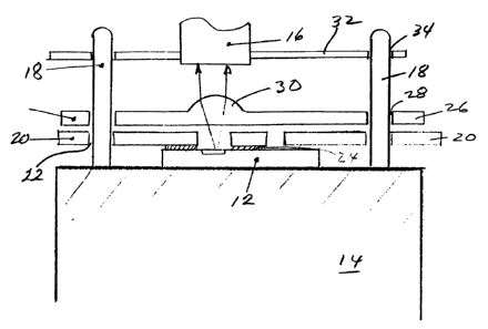
15 Figure 1 illustrates one practical embodiment of the
present invention wherein a light emitting device such as
VCSEL 12 is mounted on a substrate 14 or other suitable
carrier and the output of the VCSEL is coupled into optical
fiber 16. In Figure 1 the substrate 14 has associated with
20 it one or more guide pins 18. The VCSEL 12 may be positioned
on the substrate 14 using an alignment marker (not shown), on
the substrate such that the VCSEL is accurately positioned
relative to guide pins 18. In Figure 1 a lead frame 20 is
used to make the necessary electrical connections to at least
2s one side of the VCSEL 12. Lead frame 20 is provided with
alignment guide means 22 which as shown in Figure 1 is a hole
of a suitable diameter to allow the lead frame 20 to drop
over the guide pins 18. It is to be understood that VCSEL 12
can also be fabricated to use a flip chip type of
3o construction wherein both electrical contacts are on the same
side and may be attached to the lead frame 20 using solder
CA 02365498 2001-12-19
4
24. The lead frame 20 is placed over the guide pins 18 and
in this case it is not necessary to provide any alignment
marking on the substrate.
Lens assembly 26 is also provided with guide means 28 in
s the form of accurately positioned holes. The bubble lens 30
associated with lens assembly 26 is positioned relative to
the guide means 28 such that when the lens assembly is
mounted on the guide pins 18 the bubble lens 30 is directly
over the active or light emitting region of the VCSEL 12.
io Finally, optical fiber 16 is held in a support member 32
which again is provided with guide means 34 such that when
the fiber support is positioned over the guide pins 18 the
fiber 16 is accurately aligned with respect to the lens 30
and the active portion of the VCSEL 12.
15 Guide pins 18 of Figure 1 may be circular in cross
section, square in cross section or in fact conical.
Further, although the guide pins are seen to be associated
with the substrate 14 it will be apparent to one skilled in
the art that they may be associated with any of the other
2o components of the assembly. For example, the pins may be
part of the lens holder 26 in which case they will fit in to
the appropriate holes in the remaining elements. The pins
may be made of metal such as aluminum, an accurately etched
semiconductor material, ceramic, plastic or other materials
2s as will be apparent to one skilled in the art.
Although the guiding means are shown as being holes
through the respective elements it will be also understood
that these may simply be appropriately contoured forms such
as grooves in the edges of the various elements of the
3o assembly.
CA 02365498 2001-12-19
The guide pins 18 may also be in the form of balls, hook
type devices or clips which, as indicated above, may be
permanently associated with one of the elements or they may
be of a type which may be removed after the assembly is
s completed and appropriately secured in place.
Figure 2 shows a device similar to that which is shown
in Figure 1 except that it now comprises an optical receiver
36 such as a photo diode. In this implementation optical
energy from a downstream source (not shown) is coupled from
io the optical fiber 16 through lens 30 and onto the active
receptor 36. As in the previous aspect each of the
components is aligned relative to each other by using the
guide pins 18 which are not shown in Figure 2.
Figures 3 and 4 illustrate application wherein the
i5 alignment of the lens assembly relative to active devices is
critical. In Figure 3 the relative output of VCSEL 12 is
monitored by a photo detector 36 by reflecting a portion of
the VCSEL output back to the detector using reflective
surfaces of the accurately positioned lens 40.
2o Figure 4 is another example of a lens assembly 42
wherein the optical transmission of an edge emitting device
44 is reflected out of the assembly by the 45 degree surface
46 of the lens 42. The emission from the back facet of the
edge emitting device 44 is deflected by surface 48, and
2s reflected by surfaces 50 and 52 to the detector 36. Again,
the lens assembly 42 must be accurately positioned with
respect to the emitter 44 and monitor 36 and this accurate
positioning can be achieved using the alignment process of
the present invention.
3o Figure 5 shows a further example wherein the lens
assembly has a partially reflecting surface such that a
CA 02365498 2001-12-19
6
portion of the emission is returned to a suitably positioned
detector.
Figure 6 shows a further version of the assembly of
Figure 1. In this case a printed circuit board 60, has
s conductor rails 61 for attachment of various active
components positioned relative to the guiding means 18.
These components may be for example a VCSEL 12 (or a photo
diode for example a PIN diode), pre and/or post amplifiers
62, drive chips 64, capacitors etc.
io It will be apparent to one skilled in the art that the
basic concept of the present invention will lend itself to
the fabrication of a variety of assemblies wherein components
on one layer must be accurately aligned relative to
components on layers above and/or below. Such elements might
i5 include in addition to the above mentioned components, one or
several ways to combine/split multiple wave lengths. The
layers may also include mechanical or environmental
protection covers to protect against moist, dust etc. The
optical elements may include in additional to a lens,
2o mirrors, anti-reflective coatings or other optical layers or
fibers. -
Although the particular embodiments of the invention
have been described and illustrated it would be apparent to
one skilled in the art that various changes can be made to
2s these embodiments without departing from the underlining
concept of the invention. It is to be understood that such
variations will follow within the full scope of the invention
as defined in the appended claims.