Note: Descriptions are shown in the official language in which they were submitted.
CA 02365506 2001-08-27
WO 00/52671 PCT/GB0O/00723
ADDRESSING BISTABLE NEMATIC LIQUID CRYSTAL DEVICES
This invention relates to the addressing of bistable nematic liquid crystal
devices.
One known bistable nematic liquid crystal device is described in WO-97/14990,
PCT/GB96/02463, G1398/02806. 1, EP96932739.4 and has been described a zenithal
bistable device (ZBD TM). This device comprises a thin layer of a nematic or
long pitch
cholesteric liquid crystal material contained between cell walls. Optically
transparent
row and column electrode structures arranged in an x,y matrix of addressable
pixel
allow an electric field to be applied across the layer at each pixel causing a
switching
of the material. One or both cell walls are surface treated to permit nematic
liquid
crystal molecules to adopt either of two pretilt angles in the same azimuthal
plane at
each surface. Opposite surfaces may have pretilt in differing azimuthal
planes. The
two states are observed as a dark (e.g. black) and a bright (e.g. light grey)
state. The
cell can be electrically switched between these two states to allow
information display
which can persist after the removal of power; i.e. the liquid crystal material
is latched
into either of the two allowed states and remain in the one latched state
until
electrically switched to the other latched state.
Another bistable nematic device is described in WO99/34251, PCT/GB98/03787.
This uses grating structures to provide bistable alignment similar to WO-
97/14990 but
uses a negative dielectric anisotropy material.
CA 02365506 2010-01-07
28817-10
2
The terms switching and latching need some explanation: in
monostable nematic devices, the affect of a suitable applied electric field is
to
move the liquid crystal molecules (more correctly the director) from one
alignment
condition to another, i.e. from a zero applied voltage OFF state to an applied
voltage ON state. In a bistable device, the application of a voltage may cause
some movement of the liquid crystal molecules without sufficient movement to
cause them to permanently move into a different (one of two) state. In the
present
application, the term switch and latch are used to mean the molecules are
caused
to move from one bistable state to the other bistable state; where they remain
until
switched or latched back to the first state.
The term same azimuthal plane is explained as follows; let the walls
of a cell lie in the x, y plane, which means the normal to the cell walls is
the z-axis.
Two pretilt angles in the same azimuthal plane means two different molecular
positions in the same x, y plane.
Another bistable nematic liquid crystal device is described in GB-
2,286,467. This uses a grating alignment surface to give two stable states in
two
different azimuthal planes.
Most presently available liquid crystal devices are monostable and
are addressed using rms. addressing methods. For example twisted nematic and
phase change type of liquid crystal devices are switched to an ON state by
application of a suitable voltage, and allowed to switch to an OFF state when
the
applied voltage falls below a lower voltage level. In these devices the liquid
crystal
material responds to the rms. value of the electric field. Various well-known
addressing schemes are used; all use ac rms. voltage values. This is
convenient
because liquid crystal material deteriorate if the applied voltage is dc.
EP 569,029 describes a long pitch cholesteric liquid crystal display
having two metastable switched states. The material is first switched to a
Frederick's transition, then switched with other voltages to either of the two
metastable states. Each state lasts for about 10 seconds after voltage is
removed;
i.e. the display has (temporary) bistability providing the display is
continually
addressed.
CA 02365506 2010-01-07
28817-10
3
Another type of device is the ferroelectric liquid crystal display
(FELCD) which can be made into bistable device with the use of smectic liquid
crystal materials and suitable cell wall surface alignment treatment. Such a
device
is a surface stabilised ferroelectric liquid crystal device (SSFELCDs) as
described
by: - L J Yu, H Lee, C S Bak and M M Labes, Phys Rev Left 36, 7, 388 (1976); R
B Meyer, Mol Cryst Liq Cryst. 40, 33 (1977); N A Clark and S T Lagerwall, Appl
Phys Lett, 36, 11, 899 (1980). These device switch upon receipt of a suitable
unipolar (dc) pulse of suitable voltage amplitude and time. For example a
positive
pulse switches to an ON state, and a negative pulse switches to an OFF state.
A
disadvantage of this is that the material will degenerate under dc. voltages.
Therefore the many known addressing schemes must ensure a net zero value dc.
For example by periodically inverting all voltages.
Known addressing schemes for bistable smectic devices include
those described in EP-0,542,804, PCT/GB91/01263, EP-0,306,203, EP-
0,197,742, Surgey et al ferroelectric 1991, vol. 122 pp63-79 etc. Some use
mono
pulse strobe pulses, others bipolar strobe pulses in combination with bipolar
data
pulses.
Bistable nematic devices, as mentioned above, switch between or
latch into their two bistable states upon receipt of suitable unipolar (dc)
pulses.
This may allow use of existing addressing schemes previously used for ferro
electric bistable devices. However, the switching characteristics of bistable
nematic devices are different from that of ferro electric bistable devices.
Some embodiments of the present invention address the problem of
switching bistable nematic liquid crystal devices by providing new addressing
schemes, which take account of the different switching characteristics of
bistable
nematic devices.
According to some embodiments of this invention, this is to provide a
method of addressing a bistable nematic device formed by two cell walls
enclosing
a layer of nematic or long pitch cholesteric liquid crystal material with
electrode
structures carried by the walls to form a series of row electrodes on one wall
and a
series of column electrodes on the other wall to form a matrix of intersecting
CA 02365506 2010-01-07
28817-10
4
regions or pixels with a wall surface treatment on at least one wall providing
a
molecular alignment permitting the molecules at or adjacent the wall to align
into
two different stable states upon application of appropriate unipolar voltage
pulses,
the method comprising the steps of:
applying a row waveform to each row in a sequence whilst
simultaneously applying one of two data waveforms to each column electrode
whereby each pixel can be independently switched between two bistable states;
the row waveform having a period of at least two time slots, at least
two unipolar pulses for switching the device to a first state, and at least
two
unipolar pulses for switching the device to a second state,
both data waveforms having a period of at least two time slots with a
unipolar pulse in each time slot, with at least one data waveform shaped to
combine with the row waveform to cause a switching to one latched state
whereby each pixel can be addressed to latch into either stable state
to collectively provide a desired display, with a substantially net zero dc
voltage
applied to the device.
CA 02365506 2010-01-07
28817-10
-5-
In some embodiments, the alignment on a cell wall is arranged to give two
different
switching characteristics; namely lower voltage/time values for switching from
one
latched state to the other latched state. This may be arranged by variation of
the
height of grooves in a grating structure, and/or variation of the period of
the grating,
and/or selection of a surfactant on the grating, and/or selection of material
elastic
constants. The surfactant may be lecithin or a chrome complex surfactant.
The addressing of the device may be in two field times, one for switching to
one stable
state, and the other for switching into the second stable state. The field
times may be
identical or different in length. The device may be addressed by selectively
switching
pixels to one state in one field time and selectively switching pixels to the
other state
in the second field time. Alternatively, some or all of the pixels may be
blanked into
one state, then selectively switched to the other state. The blanking can be
done at
the same time to all pixels, a row at a time (e.g. one or more rows ahead of
selective
addressing), or the blanking and selective addressing may be combined as each
row
is being addressed.
The row waveform may be at least two unipolar pulses capable of blanking
pixels, and
at least two unipolar addressing pulses capable of combining with data
waveforms to
selectively switch pixels. The blanking pules may be of equal and opposite (or
the
same polarity) amplitude or different (including a zero) amplitude; similarly
the
addressing pulses may be of equal and opposite amplitude or different
(including a
zero) amplitude providing that overall the device receives substantially net
zero dc
voltage. The blanking pulses may be of the same or different amplitude to
those of
the addressing pulses. The two blanking pulses and the two addressing pulses
may
be equally or unequally spaced apart in time including blanking immediately
followed
by addressing. When the row waveform period is formed of three or more is
periods,
then at least one time slot may be of zero voltage amplitude.
CA 02365506 2001-08-27
WO 00/52671 PCT/GBOO/00723
-6-
Each data waveform is usually of equal and opposite alternate pulses. However,
for
some applications a zero voltage may be applied in one time slot of each
waveform
period.
The row and data waveforms may have periods of two, three, four, or more time
slots
ts. The line address time may have periods of two, three, four, or more time
slots ts.
Furthermore, the row waveform period may extend in time over more than one
line
address time, in a manner analogous to the addressing of FELCDs in EP-
0,542,804
PCT/GB91 /01263.
The addressing may be to each row in turn, or in a different sequence, such as
interleaving the addressing e.g. as in Figure 11 below.
The temperature of the liquid crystal material may be measured and voltages
Vs, Vd
ratio of VsNd and/or time length of ts, and/or relative position of blanking
to selective
addressing pulses adjusted to compensate for switching characteristics with
temperature.
Additional voltage waveforms, voltage reduction waveforms, may be added to the
row
and or column electrodes. When added to row electrodes these voltage reduction
waveforms combine with the column voltages without changing the required
switching
voltages to give an overall reduction in peak or rms. levels.
Use of voltage reduction waveforms gives reduced voltages requirements for
driver
circuits. This enables standard drivers circuits designed to rms. address
twisted
nematic type of displays, to be used as in GB 2,290,160.
CA 02365506 2010-01-07
28817-10
7
According to some embodiments of this invention, a bistable nematic
device comprises:
two cell walls spaced apart and enclosing a layer of nematic or long
pitch cholesteric liquid crystal material;
a first series of electrodes on one wall and a second series of
electrodes on the other wall collectively forming a matrix of intersecting
regions or
pixels;
surface treatments on at least one wall to provide a molecular
alignment permitting the molecules at or adjacent the wall to align into two
different stable states upon application of appropriate unipolar voltage
pulses;
means for distinguishing between the switched states of the liquid
crystal material;
means for generating and applying a row waveform to each
electrode in the first series of electrodes in a sequence;
means for generating and applying one of two data waveforms to
each electrode in the second series of electrodes;
the row waveform having a period of at least two time slots and at
least two unipolar pulses for switching the device to a first state, at least
two
unipolar pulses for switching the device to a second state;
both data waveforms having a period of at least two time slots with a
unipolar pulse in each time slot giving substantially net zero dc value, with
at least
one data waveform shaped to combine with the row waveform to cause a
switching to one latched state;
whereby each pixel can be independently switched into either stable
state to collectively provide a desired display, with a substantially net zero
dc
voltage applied to the device.
CA 02365506 2001-08-27
WO 00/52671 PCT/GBOO/00723
-8-
The means for distinguishing between the switched states of the liquid crystal
material
may be two polarisers, or a dichroic dye in the liquid crystal material with
or without
one or more polarisers. The polarisers may be neutral or coloured.
The first series of electrodes may be formed into row or line electrodes, and
the
second series of electrodes formed into column electrodes. The row and column
electrodes form collectively a x,y matrix of addressable pixels. Typically the
electrodes
are 200 m wide spaced 20 m apart. Other electrode configurations may be used.
For example so called r-O arrangements. Also alpha numeric, or seven or eight
bar
arrangements may be made.
The surface treatment may be grating surfaces. The grating may be a profiled
layer of
a photopolymer formed by a photolithographic process e.g. M C Hutley,
Diffraction
Gratings (Academic Press, London 1982) p 95-125; and F Horn, Physics World, 33
(March 1993). Alternatively, the grating may be formed by embossing; M T Gale,
J
Kane and K Knop, J App. Photo Eng, 4, 2, 41 (1978), or ruling; E G Loewen and
R S
Wiley, Proc SPIE, 88 (1987), or by transfer from a carrier layer.
The grating profile may be uniform over each complete pixel, or may vary
within each
pixel so that different voltage levels are needed to switch different areas of
a pixel.
For such an arrangement, more than two different data waveforms may be used.
CA 02365506 2001-08-27
WO 00/52671 PCT/GBOO/00723
-9-
The device may include driver circuits, logic arrays, inputs such as
keyboards, or
computer links to address the device. Alternatively, the device may be a cell
only,
with cell walls, electrodes, liquid crystal material, and surface alignment
treatment. In
the latter case, the device may include contacts for connecting to drivers
etc. as
required when changes are made to the display device. This utilises the
bistable
nature of the device. For example smart cards may display information that can
be
changed by external means such as driver circuits, radio, magnetic, or laser
readers
or addressers when inserted into control circuits etc.
Cells designed as smart cards may suffer from static effects when moved
around, e.g.
into pockets or wallets. To avoid possible static effects some or all of the
electrodes
may be connected together with resistive links. These allow a charge
stabilisation at
the electrodes to prevent unwanted changes in display. The links are of
sufficient
value to allow the induced charges to equalise slowly without effecting the
much
higher frequency voltage changes occurring when the cell is addressed.
The device may include nematic material only, or nematic plus a small amount
of a
chiral or cholesteric additive such as cholesteric liquid crystal material,
and may
include an amount of a dichroic dye for enhancing observed colour.
CA 02365506 2010-01-07
28817-10
-10-
Some embodiments of the invention will now be described, by way of example
only with reference to the accompanying drawings of which:
Figure 1 is a plan view of a matrix multiplexed addressed liquid crystal
display as
described in WO-GB96/02463;
Figure 2 is the cross section of the display of Figure 1;
Figures 3a and 3b show a cross section of a stylised cell configuration with
bistable
switching between the two states as described in WO-97/14990, the two figures
show
high and low surface tilt respectively on a bistable surface;
Figure 4 shows the transmission of the cell and the applied signals as a
function of
time;
Figure 5 shows switching characteristic of time against voltage for a bistable
nematic
device, two sets of curves are shown to indicate switching from dark to light
(upper
curve) and light to dark (lower curve), the solid lines indicate full
switching and the
broken lines indicate onset of switching;
Figure 6 shows a first example of waveforms of the present invention to
address eight
lines with four columns using two time slot addressing with strobe pulses
arranged in
two equal field addressing times;
Figure 7 shows the optical response of a pixel to resultant voltages applied
by the
addressing scheme of Figure 6;
CA 02365506 2001-08-27
WO 00/52671 PCT/GBOO/00723
-11-
Figure 8 shows the effect of changing line addressing time on transmission at
several
marked pixels to give an indication of pixel pattern dependence on the
addressing
scheme of Figure 6;
Figure 9 shows a scheme similar to that of Figure 6, but with a zero voltage
level
applied to all column electrodes in the first field time;
Figure 10 shows a two slot scheme where each line is blanked to one state then
1o switched selectively to the other state;
Figure 11 shows a two slot scheme with blanking and selective switching, where
the
rows are addressed with two interleaved fields, rather than each field in turn
as in
Figure 9;
Figure 12 shows the optical response of a pixel to resultant voltages applied
by the
addressing scheme of Figure 11;
Figure 13 shows the effect of changing line addressing time on transmission at
several marked pixels to give an indication of pixel pattern dependence on the
addressing scheme of Figure 11;
Figure 14 shows a four slot addressing scheme with blanking followed by
selective
switching and periods of zero voltages in both strobe and data waveforms; and
Figure 15 shows a three slot addressing scheme with blanking then selective
addressing and with rms. reduction waveforms applied to rows to reduce
resultant
rms. voltage value.
CA 02365506 2001-08-27
WO 00/52671 PCT/GBOO/00723
-12-
The known display in Figures 1, 2 comprises a liquid crystal cell 1 formed by
a layer 2
of nematic or long pitch cholesteric liquid crystal material contained between
glass
walls 3, 4. A spacer ring 5 maintains the walls typically 1-6 m apart.
Additionally
numerous beads of the same dimensions may be dispersed within the liquid
crystal to
maintain an accurate wall spacing. Strip like row electrodes 6 e.g. of Sn02 or
ITO
(indium tin oxide) are formed on one wall 3 and similar column electrodes 7
are
formed on the other wall 4. With m-row and n-column electrodes this forms an
mxn
matrix of addressable elements or pixels. Each pixel is formed by the
intersection of a
row and column electrode.
A row driver 8 supplies voltage to each row electrode 6. Similarly a column
driver 9
supplies voltages to each column electrode 7. Control of applied voltages is
from a
control logic 10, which receives power from a voltage source 11 and timing
from a
clock 12.
Either side of the cell 1 are polarisers 13, 13' arranged with their
polarisation axis
substantially crossed with respect to one another and at an angle of
substantially 45
to the alignment directions R, if any, on the adjacent wall 3, 4 as described
later.
Additionally an optical compensation layer 17 of e.g. stretched polymer may be
added
adjacent to the liquid crystal layer 2 between cell wall and polariser.
A partly reflecting mirror 16 may be arranged behind the cell 1 together with
a light
source 15. These allow the display to be seen in reflection and lit from
behind in dull
ambient lighting. For a transmission device, the mirror 16 may be omitted.
Alternatively, an internal reflecting surface may be used.
CA 02365506 2001-08-27
WO 00/52671 PCT/GBOO/00723
-13-
Prior to assembly, at least one of the cell walls 3, 4 are treated with
alignment gratings
to provide a bistable pretilt. The other surface may be treated with either a
planar (i.e.
zero or a few degrees of pretilt with an alignment direction) or homeotropic
monostable surface, or a degenerate planar surface (i.e. a zero or few degrees
of
pretilt with no alignment direction).
The grating surfaces for these devices can be fabricated using a variety of
techniques
as described in WO-97/14990. The homeotropic treatment can be any surfactant,
which has good adhesion to the grating surface. This treatment should also
lead to an
unpinned alignment. That is, an alignment which favours a particular nematic
orientation without inducing rigid positional ordering of the nematic on the
surface.
Finally the cell is filled with a positive dielectric anisotropy nematic
material which may
be e.g. E7, ZL12293 or TX2A (Merck). Alternatively the material may be a
negative
dielectric anisotropy nematic material such as ZLI 4788, ZLI.4415, or MLC.6608
(Merck).
Small amounts e.g. 1-5% of a dichroic dye may be incorporated into the liquid
crystal
material. This cell may be used with or without a polariser, to provide
colour, to
improve contrast, or to operate as a guest host type device; e.g. the material
D124 in
E63 (Merck). The polariser(s) of the device (with or without a dye) may be
rotated to
optimise contrast between the two switched states of the device.
CA 02365506 2001-08-27
WO 00/52671 PCT/GBOO/00723
-14-
One suitable cell configuration to allow switching between the bistable states
is shown
in Figure 3 which is a stylised cross section of the device in which a layer 2
of nematic
liquid crystal material with positive dielectric anisotropy is contained
between a
bistable grating surface 25 and a monostable homeotropic surface 26. The
latter
surface 26 could, for example, be a flat photoresist surface coated with
lecithin.
Within this device liquid crystal molecules can exist in two stable states. In
state (a)
both surfaces 25, 26 are homeotropic whereas in (b) the grating surface 25 is
in its
low pretilt state leading to a splayed structure. Either state may be bright
or dark
depending on orientation of polarisers, bulk twist angle and cell geometry
(transmissive/reflective). The convention adopted in this application is to
define the
OFF state of Figure 3a as a dark (or black) state, and that of Figure 3b the
bright (or
light) state. For many nematic materials, a splay or bend deformation will
lead to a
macroscopic flexoelectric polarisation, which is represented by the vector F
in Figure
3. A dc pulse can couple to this polarisation and depending on its sign will
either
favour or disfavour configuration (b).
With the device in state (a), the application of a positive pulse will still
cause
fluctuations in the homeotropic structure despite the positive dielectric
anisotropy.
These fluctuations are sufficient to drive the system over the energy barrier
that
separates the two alignment states. At the end of the pulse the system will
fall into
state (b) because the sign of the field couples favourably with the
flexoelectric
polarisation. With the system in state (b), a pulse of the negative sign will
once again
disrupt the system but now it will relax into state (a), as its sign does not
favour the
formation of the flexoelectric polarisation. In its homeotropic state, the
bistable surface
is tilted at slightly less than 900 (e.g. 89.5 ). This is sufficient to
control the direction of
splay obtained when the cell switches into state (b).
One particular cell consisted of a layer of nematic ZL12293 (Merck) sandwiched
between a bistable grating surface and a homeotropic flat surface. The cell
thickness
was 31-Lm. Transmission was measured through the cell during the application
of dc
pulses at room temperature (20 C). The polariser and analyser 13, 13' on each
side
of the cell 1 were crossed with respect to each other and oriented at 45 to
the
CA 02365506 2001-08-27
WO 00/52671 PCT/GBOO/00723
-15-
grating grooves. In this set up, the two states in Figure 3, (a) and (b),
appear dark
(black) and bright (light) respectively when addressed as follows.
Figure 4 shows the applied voltage pulses (lower trace) and the optical
response
(upper trace) as a function of time. Each pulse had a peak height of 55.0
volts and a
duration of 3.3ms. Pulse separation was 300ms. With the first application of a
positive
pulse, the transmission changes from dark to light indicating that the cell
has switched
from state Figure 4(a) to state (b). A second positive pulse causes a
transient change
in transmission due to the rms. effect of coupling to the positive dielectric
anisotropy
causing a momentary switching of the bulk material to state (a). However, in
this case
the cell does not latch at the surface and so remains in state (b). The next
pulse is
negative in sign and so switches the cell from state (b) to state (a). Finally
a second
negative pulse leaves the cell in state (a). This experiment shows that the
cell does
not change state on each pulse unless it is of the correct sign. Thus it
proves that the
system is bistable and that the sign of the applied pulse can reliably select
the final
state.
Figure 5 shows typical switching characteristics. Four lines are shown, the
upper full
line and upper broken line indicate the time/voltage curves when switching
from dark
to light; the broken curve indicates the onset of switching, the full curve
indicates
complete switching. The region between the full curve and broken curve is a
partial
switch region. The lower two lines indicate the same features for switching
from light
to dark. Time/voltage values above the full curve always switch. As shown, for
a
particular value of timer a pulse of negative Vs (or -(Vs-Vd) or -(Vs+Vd))
will switch
all pixels to dark; but a pulse of +Vs by itself is not sufficient to fully
switch to light.
Thus to switch to bright requires +(Vs+Vd), i.e. the strobe pulse plus the
appropriate
data pulse is required.
The partial switching region may be exploited to partially switch pixels and
thereby
generate levels of grey scale in an analogue fashion. For example the data
waveform
amplitudes, Vd, may be modulated in such a way that the resultant strobe plus
data
pulse falls within the dark to bright partial switching region in a controlled
manner. If
the strobe and data voltages were such that (Vs-Vd) lay on the onset of
switching
curve and +(Vs+Vd) lay on the full switching curve then varying the amplitude
of the
CA 02365506 2001-08-27
WO 00/52671 PCT/GBOO/00723
-16-
data voltage from zero to Vd would give controlled partially switched levels
of
brightness for resultant pulses of +(Vs Vd) whilst resultant pulses of -(Vs
Vd) would
always switch to dark.
These curves contrast with e.g. FELCDs where switching characteristic curves
vary
with the shape of applied voltages, but not with the direction of switching.
The
distance apart of the two curves can be varied by varying the height of the
grating
surface, and/or varying the amplitude of the grating, and/or varying surface
anchoring
energy, e.g. by use of different surfactants. This has the effect of changing
the energy
level of the two permitted states. By this means, the two curves can be made
to occur
even further apart, to coincide or even reverse their positions.
One possible explanation for this separation of the two curves is that
switching to
black utilises both flexo electric dielectric coupling to the applied field
(for a positive
dielectric anisotropy material), whereas in switching to the white state there
is
coupling to the flexo electric constant only. The shape of the grating surface
is
selected to give slightly different energy levels in the two states to allow
for this, or
even enhance the difference between switching voltages. In one typical example
the
value of grating height h to period w h/w was 0.6; typically the range is 0.5
to 0.7.
Typically h is 0.5 in a range of 0.1 to 10 m, w is 1 in a range 0.05 to 5 m.
In the
device of WO-97/14990 h/w was 0.6. For low h/w, the high pretilt state has the
lowest
energy and so the nematic will preferentially adopt a high pretilt state,
Figure 3a.
Conversely for large h/w, the low pretilt state has the lowest energy and
nematic will
preferentially adopt this state. Around h/w=0.52 the two states have the same
energy.
Arranging h/w away from this condition separates the two switching curves of
Figure 5. Additionally or alternatively, the surface surfactant may be varied.
CA 02365506 2001-08-27
WO 00/52671 PCT/GB0O/00723
-17-
The characteristics shown in Figure 5 can be obtained in a test cell (e.g. a
single pixel
cell) by application of suitable voltage pulses. In a matrix cell with many
pixels, e.g.
Figure 1, voltages are applied by application of row waveforms to each row in
a
sequence at the same time that one of two data waveforms are applied to each
column. This requires designing the shape of the row and column waveforms to
achieve the desired result. Several different shapes and arrangements are
possible
and are described below. A common feature is the need to achieve substantially
net
zero dc voltage at each pixel. This is usually achieved using waveforms with
pairs of
equal and opposite unipolar pulses, even though for addressing purposes only,
single
pulses would be adequate.
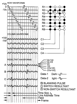
Figure 6 shows a first example of the present invention. A four column by
eight-row
matrix is addressed into the particular pattern shown with full circles the
OFF dark
state and the empty circles the ON light state.
All waveforms are time divided into time slots ts. The time taken to address
each line
is 2ts and is termed the line address time. The time taken to address a
complete
display is termed a frame time, made up (in the specific example of Figure 6)
of two
field times.
Addressing is by way of row waveforms applied in a sequence to each row in
turn,
together with one of two data waveforms applied to each column. The row
waveform
is formed of a first pulse of voltage +Vs in a is immediately followed by a
pulse of -Vs
in one is in a first field followed sometime later by the inverse in a second
field. In the
context of Figure 6, the four pulses of amplitude Vs are termed strobe pulses.
In the
technical field of FELCD's, the term strobe is used for a (row) pulse which
combines
with a data (column) pulse selectively to effect pixel switching; whilst the
term blanking
pulse is used for a (row) pulse that always causes a pixel to switch
irrespective of the
data pulse applied to a column. Often the blanking pulse is significantly
larger in
amplitude and/or time than strobe pulses. For the eight-row display of Figure
6, the
field time is 8x2ts and therefore the frame time is 2x8x2ts.
CA 02365506 2001-08-27
WO 00/52671 PCT/GBO0/00723
-18-
The two data waveforms are the same but opposite polarity, one (shown as data-
1) is
used when switching to a dark state, the other (shown as data-2) to switch to
a light
state when combined with an appropriate strobe. Each data waveform consists of
pulses of either +Vd or -Vd in successive time slots.
Marked on the Figure 6 are pixels, row and column intersections, R3/C1, R3/C2,
R3/C3, R3/C4 marked A, B, C, D respectively.
Column waveforms applied to columns C1 to C4 are shown. Since all pixels in C1
remain in the OFF dark state, the data waveform for C1 remains the same data-1
for
the whole addressing time. In column C2 the pixels are alternately OFF and ON,
and
therefore the waveform applied to C2 is alternately data-1 and data-2. For C3
the
column waveform is data-2, data-1, data-1, data-2, data-2, data-1, data-1, and
data-2
in successive line address times of 2ts. Column C4 receives data-1, data-1,
data-2,
data-2, data-1, data-1, data-2, data-2 in successive line address times.
Resultant waveforms appearing at pixels A, B, C, D, are as shown. For pixel A
the
strobe in the first field time is used with data-1 to cause a switching to
dark with the
second of the strobe pulses in ts6 giving a resultant of -(Vs+Vd). Examination
of
Figure 5 shows that a pixel can be switched from light to dark at a voltage
time
product between the two curves. The combination of either -(Vs+Vd) or -(Vs-Vd)
can
be arranged in the first field time to lie between the two curves and cause
switching to
dark. This means that the data waveform in this first field can be either data-
1 or
data-2. Data-1 is used in the particular example of pixel A Figure 6.
Therefore, to use
the terminology of FELCD's the first two strobe pulses are blanking pulses
even
though they are of the same amplitude as the true strobe pulses. Later, for
pixel A in
the second field time, the resultant +(Vs-Vd) is not sufficient to cause
switching from
OFF to ON because it lies between the two curves of Figure 5 and therefore
below the
value required to switch from dark to light.
CA 02365506 2001-08-27
WO 00/52671 PCT/GBOO/00723
-19-
Pixel B is switched by resultant -(Vs-Vd) to dark (because of a lower
amplitude
required to switch to dark than to bright) in ts6 of the first field time and
to bright in the
second field time by the resultant +(Vs+Vd) in the second pulse of the second
strobe
pulse pair in ts22. Similarly, (like pixel A) pixel C is switched to dark in
the first field
time and remains dark in the second field time. Pixel D (like pixel B) is
switched to
dark in the first field time and to light in the second field time.
Separation of the curves allows a strobe pulse to function as a blanking
pulse. One
disadvantage for some two-field schemes is that the bright state has a reduced
average value because e.g. pixels B and D are always switched to dark in one
field
and bright in the second field. Bringing the two curves of Figure 5 together,
allows the
voltage levels to be adjusted e.g. so that bright pixels can remain bright in
the first
field with increase average transmission levels.
The example shown in Figure 6 uses two field times of equal time duration, the
first
field is used to switch to the OFF dark state, and the second field is used to
switch to
the ON light state. Throughout both first and second field times, data-1 or
data-2 is
applied to each column. This has a disadvantage of maintaining a high rms.
level of
voltage at each pixel. Display contrast is reduced with increasing rms.
levels.
Figure 7 shows the response of a pixel to the resultant waveforms of Figure 6;
the
applied waveform is at the top and the optical response shown below. Test
details
were as follows: Vs=15v, Vd=4v, line address time = 10ms, material Merck BL-
036,
thickness approximately 4 m. At time zero the pixel is in the bright state but
transmission is small due to the rms. signal caused by the column waveforms at
a
pixel in its light state. A large dc pulse switches the pixel to its dark
state and the
transmission drops to a low value within the time shown as address dark frame.
If the
pixel then receives zero voltage, the transmission is seen to drop even
further; this is
indicated as a time of zero bias frame.
CA 02365506 2001-08-27
WO 00/52671 PCT/GBOO/00723
-20-
During the second field time, indicated as address bright frame, an amount of
rms. is
received due to the column waveforms, then an address to light state pulse is
received and causes an increase in transmission indicating that the pixel has
switched
to its light state. If the pixel then receives zero voltage, indicated as zero
bias frame,
then the transmission increases considerably to a higher level.
Two features are observed. First the pixel switches and latches into two
stable states,
the dark and light states. Second the presence of rms. voltage across a pixel
reduces
the contrast between dark and light states. Thus the best display occurs when
all
pixels are latched to their required dark or light state, and when all
voltages are
removed from the device. For some devices where information to be displayed is
changed infrequently, such an addressing scheme is adequate. For example
credit
card type displays which are only changed at sales transactions.
Figure 8 shows light transmission for each pixel A, B, C, D in Figure 6
plotted against
changes in line address time (I.a.t.). The addressing scheme of Figure 6 had
Vs=15v,
Vd=4v with 32 lines addressed. When line address time is around 8 or
9mseconds,
all four pixels will switch fully. Either side of this time, some pixels will
switch partly,
thereby indicating what is termed pixel pattern dependence. Thus for the
scheme of
Figure 6, to obtain maximum usefulness, the line address time must be adjusted
so
that a clear display is obtained whatever pattern of dark and light pixels is
required.
Figure 9 is similar to that of Figure 6, except that throughout the entire
first field time,
the column waveform is held at zero volts. As a result the maximum voltage at
pixels
A, B, C, D during the first field time are +Vs and -Vs. This level is arranged
to be
sufficient to switch all to the dark OFF state when -Vs is received. In the
second field
time, all pixels required to be ON are switched to ON by the pulse +Vs+Vd. For
pixel
B and D this has the disadvantage that pixels B, and D are switched to OFF for
one
field time then to ON in the second field time; this reduces their average
brightness.
CA 02365506 2001-08-27
WO 00/52671 PCT/GBOO/00723
-21-
In a modification (not shown) of Figure 9, the two strobe pulses in the first
field are
applied to each row at the same time, thereby reducing the first field to as
low as 2ts,
but can be made longer. At the same time either a zero or a data-1 or modified
data
is applied to all columns. Then, in a second field as for Figure 9, the
remaining strobe
pulses and either data-1 or data-2 are applied to respective rows and columns
to
cause selective switching. Such an addressing scheme can be termed blanking
followed by selective switching in one field; it reduces the frame time.
A variation of total blanking in one line address time then selective
switching, is to
blank then selectively address each row in turn. This is shown in Figure 10
where
each row is blanked 2 line address times ahead of selective addressing. In the
particular example of Figure 10 the blanking pulses are of the same amplitude
as the
strobe. For example, at row R3, the blanking (after receiving +Vs for tsl) is -
Vs in ts2,
which switches all pixels to dark irrespective of which data waveform is being
applied.
This is shown in the resultant waveforms where all pixels in row R3 switch in
the first
two time slots.
In the particular example of Figure 10 the blanking is 2 line addressing times
ahead of
the strobe; other values can be chosen. For example, the blanking may
immediately
precede the two strobe pulses, or may be several line addressing times ahead.
Thus in R3, after the second blanking pulse of -Vs has been applied, there is
zero for
both ts3 and ts4. The strobe of -Vs for ts5, and +Vs for ts6 is applied in
combination
with the appropriate data as shown under column waveforms during periods ts5,
M.
As before the strobe waveform, comprising the two blanking pulses and the two
strobe pulses, is applied to each row R1 to R8 in turn. The total address time
is 8 line
address times, i.e. 16ts in contrast with 32ts for the schemes of Figures 6,
7.
CA 02365506 2001-08-27
WO 00/52671 PCT/GB00/00723
-22-
Examination of the resultants show: -
For pixel A, large blanking +(Vs+Vd) then -(Vs+Vd), then +Vd, -Vd (the time
between
blanking and strobe addressing), then -(Vs-Vd) and +(Vs-Vd) in ts5, M. These
values Vs-Vd are insufficient to cause switching from the blanked dark to
light
because Vs-Vd lies between the two curves in Figure 5 and the material will
not
switch to light.
For pixel B, blanking by +(Vs-Vd) then -(Vs-Vd). This will switch to dark
because the
Vs-Vd lies between the curves of Figure 5 (i.e. above the curve switching to
dark) and
the material will switch to dark. Later in ts5, ts6, the resultant of -(Vs+Vd)
then
+(Vs+Vd) switches to light because Vs+Vd is above the dark to light switching
curve
of Figure 5.
In the time periods ts5, ts6 the difference between pixels A and B is that the
data
waveform for pixel A is different to that of pixel B. This allows the
selective switching
of pixels from dark to light depending upon the data waveform used in
combination
with the strobe pulses.
For pixels C and D the situation is similar to that for pixels A and B, namely
switching
to dark by the blanking in tsl, ts2 and selective switching to light in ts5,
ts6.
In the scheme of Figure 10 the whole device is addressed in a single field,
the field
and frame time are the same. In another embodiment, each row is blanked then
selectively addressed at least twice per frame time; i.e. each row is
addressed two or
more times in two or more fields per frame. A similar scheme is described for
FELCDs in WO-95/27971.
CA 02365506 2001-08-27
WO 00/52671 PCT/GBOO/00723
-23-
Figure 11 shows a two slot addressing scheme in which first and second fields
are
interleaved and each pixel is blanked to black then selectively switched to
light. The
row waveform is a blanking formed by +Vs then -Vs in adjacent time slots,
followed by
zero volts for 4ts, then addressing strobes of -Vs and +Vs in adjacent times
slots. In
this example the blanking pulse and addressing strobe pulse are of equal
value, but
they could be different.
Data waveforms are -Vd then +Vd for dark switching, and +Vd then -Vd for light
switching. When a particular row is blanked the data value is zero on all
columns
since there is no need for selectivity of data and the pixel will switch dark
under -Vs
only.
Addressing of R3 is as follows: for time periods ts5, ts6 the strobe waveform
is +Vs
then -Vs, the row waveforms are zero on all columns C1 to C4, giving
resultants of
+Vs then -Vs at each pixel A, B, C, D which gives a blanking level switching
to dark in
M. For time slots ts7 and ts8 the resultant at pixels A, B, C, D is +Vd then -
Vd, which
is below any switching level. For time slots ts9 and tsl0 the resultants at
pixels A, B,
C, D are zero because the row 3 waveform is zero and all the columns are at
zero
while row 4 is being blanked. For time slots tsl 1 and ts12 the addressing
strobe is -
Vs then +Vs, the data waveform is -Vd then +Vd on C1 and C3, and +Vd then -Vd
on
C2 and C4. The resultant at pixels A and C is -(Vs-Vd) then +(Vs-Vd) which is
insufficient to cause switching from dark to the bright state. The resultant
at pixels B
and D is -(Vs+Vd) then +(Vs+Vd) which is sufficient in ts12 to cause a
switching to
bright.
CA 02365506 2001-08-27
WO 00/52671 PCT/GBOO/00723
-24-
The effect of interleaving is as follows: immediately after R3 is blanked,
i.e. ts7 and
ts8, row R2 is selectively addressed to the light state by the strobe pulse of
-Vs then
+Vs whilst data levels of +/-Vd are applied to each C1 to C4. This is followed
in time,
i.e. ts9 and ts10, by blanking pulses of +Vs then -Vs applied to R4 whilst
zero data
voltage is applied to columns C1 to C4. Thus addressing is as follows: (e.g.
starting
at row R3) blank R3, selectively address R2, blank R4, selectively address R3,
blank
R5, selectively address R4, blank R6, selectively address R5, blank R7,
selectively
address R6 etc. The effect of interleaving is to reduce the time between the
dark and
the light state for pixels required to be in the light state, and also to
reduce the rms.
level at each pixel due to the zero voltage during some time periods.
Figure 12 shows a pixel's optical response, lower trace, to applied voltages,
upper
trace, for the addressing scheme of Figure 11; Vs=15v, Vd=4v, I.a.t.=20ms, 32
lines of
addressing. At time zero the pixel is in its light state and receiving a small
rms.
voltage from the data waveforms. Within the time marked address dark frame the
pixel receives a blanking -Vs pulse which causes switching to the dark state
and a
large reduction in optical transmission. During the time marked address bright
frame
a large switching pulse of Vs+Vd causes a switching to the light state and a
large
increase in optical transmission which increases further during the time
marked zero
bias. Comparison of Figure 12 with that of Figure 7 shows a much improved
contrast
between dark and light state particularly during the time when an rms. voltage
appears at a pixel. Therefore the addressing scheme of Figure 11 is better
than that
of Figure 6 for displays requiring continual updating of information.
Additionally, as shown in Figure 13, the range of line address times over
which the
pixels A, B, C, D switch is much superior to that in Figure 8. Clear switching
is
obtained from about 12ms to about 35ms. This shows the scheme of Figure 11 is
relatively insensitive to pixel pattern irregularity.
CA 02365506 2001-08-27
WO 00/52671 PCT/GBOO/00723
-25-
The addressing schemes of Figures 6-11 are two slot schemes, i.e. both strobe
and
data waveforms are two pulses period.
Figure 14 shows a four slot scheme with blanking. In this the row waveform is
zero,
+Vs, -Vs, zero to give blanking, and zero, -Vs, +Vs, zero to give strobe
pulse. The
column waveform is zero, -Vd, +Vd, zero to give selective switching to dark,
and zero,
+Vd, -Vd, zero to give selective switching to light. As shown blanking and
strobe
pulses are of the same amplitude but could be different. The gap between the
end of
the blanking and the start of a strobe is 4ts time periods but could be longer
or
shorter.
For pixel A the resultant is zero, +(Vs+Vd), -(Vs+Vd), zero in periods tsl to
ts4 giving
blanking to dark in W. In periods ts9 to ts12 the voltages are zero, -(Vs-Vd),
+(Vs-
Vd), zero which does not switch to bright and the pixel A remains dark as
required.
For pixel B the resultant is zero, +(Vs-Vd), -(Vs-Vd), zero in tsl to ts4
which is
sufficient to blank to dark in period ts3. In periods ts9 to ts12 the voltage
is zero, -
(Vs+Vd), +(Vs+Vd), zero which switches to light in tsl 1 as required.
Similarly for pixels C, D, both are blanked to dark in ts3 and pixel D is
selectively
switched to light in tsl 1.
Inspection of the resultant waveforms shows a short time between switching
from dark
to light where required, and zero voltage for some periods thereby reducing
the rms.
level.
CA 02365506 2001-08-27
WO 00/52671 PCT/GBOO/00723
-26-
Both two and four slot addressing schemes have been described above. It is
also
possible to have an odd number of slots. This is shown in Figure 15, which is
a
blanked three slot scheme with a voltage reduction waveform applied to rows
only.
The row waveform is zero, +Vs, -Vs in three successive is periods to give a
blanking
voltage, then zero, -Vs, +Vs in three successive is periods to give selective
addressing to light when combined with an appropriate data waveform. Between
the
end of the three blanking pulses and the start of the three selective
addressing pulses
is a period of 3ts, but this could be more or less. Again the blanking and
strobe
amplitude levels are the same but could be different. In between the strobe
pulses is
a voltage reduction waveform. This applies -Vd/2, +Vd, and -Vd/2 in each three
time
slot period.
The data waveforms are -Vd, +Vd, zero in three adjacent time slots to give
switching
to dark state; zero, +Vd, -Vd in three adjacent time slots to give switching
to light.
In row R3 all pixels A to D are blanked to dark within the period tsl to ts3,
then pixels
B and D are selectively switched to light within the period ts7 to ts9. During
the period
ts4 to ts6 the previously blanked R2 is selectively switched to light.
For pixel A the resultant voltages are -(O-Vd), +(Vs-Vd), -(Vs-0) in tsl, ts2,
ts3 giving a
blanking to dark in ts3. In periods ts7, ts8, ts9 the resultant voltages are -
(O-Vd), -
(Vs+Vd), (Vs-0) without switching from dark.
For pixel B the resultant voltages are 0-0, +(Vs-Vd), -(Vs-Vd) in ts1, ts2,
ts3 giving a
blanking to dark in ts3. In periods ts7, ts8, ts9 the resultants are -(0-0), -
(Vs+Vd),
+(Vs+Vd) giving selective switching to light in period M.
CA 02365506 2001-08-27
WO 00/52671 PCT/GBOO/00723
-27-
Similarly for pixels C and D, they both blank to dark in ts3, and pixel D
selectively
switches to light in ts9.
Outside of the blanking and selective switching periods, the resultant
waveform is
reduced due to the presence of the voltage reduction waveform on the rows (-
Vd/2,
Vd, -Vd/2) combining with data waveforms values (0, Vd, -Vd) giving resultants
of -
Vd/2, 0, Vd/2 or Vd/2, 0, -Vd/2. The complete resultant waveform has a reduced
r.m.s. level.
Examples of the effect of using voltage reduction waveforms follows:
Appendix A.
Calculation of r.m.s. values of waveforms with and without row reduction
waveform of
Figure 14.
Let the display have N rows.
The blanking pulse resultant may be one of two values -
Vd, Vs-Vd, -Vs or 0, (Vs-Vd), -(Vs-Vd)
These give mean square values over the N-way addressing cycle of -
B, = ((Vd2/3 +(Vs-Vd)2/3 +Vs2/3)/N or B2 = (2 (Vs-Vd)2/3)/N
Similarly the ON and OFF strobe resultants are -
0, -(Vs+Vd), (Vs+Vd) and Vd, -(Vs+Vd), Vs
giving mean square values over the N-way addressing cycle of -
SON = (2 (Vs+Vd)2/3)/N or SOFF = (Vd2/3 +(Vs+Vd)2/3 +Vs2/3)/N
CA 02365506 2001-08-27
WO 00/52671 PCT/GBOO/00723
-28-
The data waveform resultants are -
-Vd, Vd, 0 and 0, Vd, -Vd
giving mean square values over the N-way addressing cycle of -
D = (2 Vd2/3) (N-2)/N for both cases.
For example, if N=128, Vs=20 and Vd=4 then
131=1.75, B2=1.333, SON=3, SOFF = 2.583 D =10.5
The possible r.m.s. values over the N-way addressing cycle are -
ONRõS = (B1 + SON + D)112 = 3.905 or ONrtõS = (B2 + SON + D)112 = 3.851
OFF.. = (B1 + SoFF + D)112 = 3.851 or ON,Tõs = (B2 + SOFF + D)12 = 3.796
If the r.m.s. reduction waveform is now included the data waveform resultants
become
-Vd/2, Vd/2, 0 and 0, Vd/2, -Vd/2
giving mean square values of -
DR = (2 (Vd2/4)/3) (N-2)/N for both cases,
which, using the example figures above is DR = 2.625.
Since there is no change in the blanking and strobe resultants the possible
r.m.s.
values over the N-way addressing cycle become -
ONrtõS = (B1 + SON + DR)1'2 = 2.715 or ON.. = (B2 + SON + DR)1'2 = 2.637
OFFm,s = (B1 + SOFF + DR)1'2 = 2.637 or ONm,s = (B2 + SOFF + DR)1'2 = 2.557
i.e. there is a reduction in the r.m.s. voltage of -1.2V in a voltage of -
3.8, a reduction
of -31 %.