Note: Descriptions are shown in the official language in which they were submitted.
CA 02366531 2001-10-10 PCT/AU00/00315
Received 30 May 2001
- 1 -
APPARATUS AND METHOD
FOR ELECTRICAL MEASUREMENTS ON CONDUCTORS
Field of the Invention
This invention relates broadly to developments
concerning equipment for electrical measurements on
conductors. The invention will be described herein with
reference to fault indicators for power distribution
cables, it will be appreciated, however, that the
invention does have broader applications, including for
example in stand alone current measurements on electrical
conductors.
Background of the Invention
Equipment for detection and location of faults on
power lines involve typically the measurement of the
magnetic fields produced by the alternating current in
power lines, using a single magnetic field sensing coil.
In substations, this involves expensive current
transformers, which must also provide insulation between
the power line conductor and earth potential.
There is also equipment which can be located
throughout a network which does not provide its own
insulation between the phase and earth potential because
it is mounted either at phase potential or at earth
potential.
Such equipment normally derives a signal
proportional to the average or peak magnetic field by
rectifying the waveform to produce a DC voltage and this
is used for the detection and location of faults. By
deriving a signal proportional to the average or peak
magnetic field, other waveform parameters, phase, and
harmonic content information is removed from the signal.
DC voltages are suitable for analogue amplification, for
AMENDED SHWE
PWAU
CA 02366531 2001-10-10 PCT/AUOO/00315
Received 30 May 2001
- la -
operating analogue control devices and for interpretation
by analogue comparators.
When the power lines experience a fault, high
currents flow in the conductors of the lines, producing a
rapid increase in the magnetic fields around the
conductors. Therefore, if an increase is detected by the
equipment, this is indicative of a fault current having
passed the magnetic field sensing coil. Typically, within
the equipment a derivative of the output signal of the
magnetic
AMIENDE SHEe,
IPENAU
WO 00/62084 CA 02366531 2001-10-10 PCT/AUOO/00315
- 2 -
field sensing coil is produced in an analogue electronic
circuit, to detect increases in the amplitude of current
flow. The currents flowing in the conductors of the power
lines, particularly during a fault situation, may typically
vary between 5 to 25,000 Amperes. The average magnetic
field around the power line conductors therefore has a high
dynamic range, which is typically between 1 to 10,000.
The types of coil which may be used to measure
magnetic fields in such equipment are i) air-cored coils
which are typically cylindrical, ii) air-cored toroids,
iii) coils, cylindrical or toroidal, which are cored with a
ferromagnetic or paramagnetic medium other than air. Each
type of coil has specific advantages and disadvantages.
Air-cored coils do not saturate in the presence of high
magnetic fields and can therefore be used to detect
magnetic fields with a high dynamic range. However, with
air-cored coils, particularly cylindrical coils mounted at
earth potential some distance from the power line
conductor, low magnetic fields generate only low induced
signals in the coil and may therefore be difficult to
detect accurately, in particularly when background signals
may contribute to the measurements.
On the other hand, coils cored with a para- or
ferromagnetic medium, increase the induced signal in the
coil due to the high permeability which results in an
increase of the magnetic field inside the coil due to
magnetic polarisation of the medium. However, such coils
have the disadvantage of saturating once the "true"
magnetic field to be measured exceeds a particular value,
and therefore the characteristics of fields in excess of
that particular value cannot be measured with such coils.
In the equipment for detection and location of faults
on power lines, the average magnetic field signal derived
from the coils is processed using an analogue cir(,,Fuit.
Some fault detectors may employ an analogue varia}53e gain
= CA 02366531 2001-10-10
PCT/AU00/00315
Received 30 May 2001
- 3 -
control utilising for example a variable resistor such as
a Junction Field Effect Transistor (JFET) to increase the
dynamic range for the measurement, however, due to the
analog nature of such circuits the output signal is then
not directly representative of measured magnetic field
strength. In some fault detectors, such as those
described in US Patent No. 4947126 and US Patent
No.5270898, a gain may be employed which is switched
between a high and low value by analogue circuitry
utilizing for example, switches or relays. However, due
to the analogue nature of such circuits, a dynamic range
of greater than 16:1 is difficult to attain and scaling of
the amplitude is normally lost. The amplitude of the
signal in the sensing coil and that of the output signal
lose their one-to-one relationship and this cannot be
restored using analogue circuitry alone.
The equipment described above has the limitation of
providing little information on the magnetic field,
waveform, phase or harmonic content and electric field
waveform, phase or harmonic content preceding, during and
after the fault, since the information utilised is
substantially limited to the identification of sudden
changes in the amplitude of the magnetic field detected by
the magnetic field sensing coil. The further information
about the magnetic field and electric field preceding,
during and after the fault can be useful in determining
the characteristics of the fault. These characteristics
include the severity of the fault (ratio of fault current
to pre-fault current), the time and duration of the fault
current and the time for the protection equipment to
operate, whether the fault was phase to phase or phase to
earth, and whether the fault current was accompanied by a
AMENDED SHEE`~
N EA/AU
CA 02366531 2001-10-10 PCT/AUOO/00315
Received 30 May 2001
- 4 -
fuse or circuit breaker operation (loss of voltage) or a
substantial variation in the voltage.
Furthermore, the equipment described above is not
able to discriminate between a fault current and what is
referred to as magnetising inrush currents, which are
typically observed when voltage is applied to a non-
faulted power system following an extended outage period.
Therefore, when the equipment detects loss of system
voltage, it usually inhibits its detection of faults until
a predetermined period after voltage is reapplied,
resulting in a period during which fault detection for the
power line concerned is impossible.
Summary of the Invention
In accordance with a first aspect of the present
invention there is provided a method for measuring at
least one characteristic parameter of an alternating
current in a conductor, the method comprising the steps
of:
- measuring the magnetic field around the
conductor at a point along the conductor;
- deriving an analogue voltage signal
representative of the measured magnetic field;
- adding a direct current (DC) offset signal to
an alternating current (AC) component of the measured
magnetic field;
- amplifying the analogue voltage signal;
- converting the amplified voltage signal into
a digital voltage signal;
- measuring the digital voltage signal and,
when the amplitude of digital voltage signal reaches a
predetermined value, adjusting a gain setting of the
amplification; and
- generating an output signal representative of
the parameter of the alternating current
-s,viENDEd SHEtz
1PEO!/AU
CA 02366531 2001-10-10 PCT/AUOO/00315
Received 30 May 2001
- 5 -
based on the amplified voltage signal and the gain
setting.
The step of adding a DC offset signal allows for
making the measured magnetic field suitable for
amplification while substantially maintaining waveform
information.
Accordingly, in at least preferred embodiments of the
present invention, a large dynamic range can be realised
for the magnetic field/alternating current measurements.
Preferably, the method can be used in conjunction with an
air-cored coil not to be limited by a saturation effect.
The characteristic parameter of the alternating
current may be one of the group of waveform
characteristics of the alternating current such as
amplitude of the alternating current; frequency of the
alternating current; phase of the alternating current;
harmonic content of the alternating current; and a
derivative of the alternating current. More than one
parameters may be measured simultaneously.
The method may preferably further comprise the step
of integrating the analogue voltage signal for obtaining
the waveform of the alternating current in the conductor.
Thereby, in at least preferred embodiments of the
present invention, even low magnetic field strengths may
be measured at high gain settings.
In one embodiment, the step of adding a DC offset
signal comprises the step of varying the DC offset signal
in response to a DC component in the digital voltage
signal.
In a preferred embodiment, the method further
comprises the step of digitally filtering the digital
voltage signal to determine the ratio of a mains voltage
signal at a mains frequency of the conductor and an
~JE SHE
IPEA/Al9
CA 02366531 2001-10-10 PCT/AUOO/00315
Received 30 May 2001
- 6 -
harmonic voltage signal at an harmonic of the mains
frequency. In one embodiment, a second harmonic is
utilised for determining whether a magnetic field signal
around the conductor is caused by magnetising inrush
current.
Preferably, the method further comprises the step of
measuring an electric field in the vicinity of the
conductor; and deriving a second analogue voltage signal
representative of the measured electric field in the
vicinity of the conductor.
In one embodiment, the step of measuring the electric
field comprises the step of placing a capacitor
arrangement in the vicinity of the conductor; and the
method further comprises the steps of amplifying the
second analog voltage signal; converting the amplified
second voltage signal into a second digital voltage
signal; measuring the second digital voltage signal and,
if the amplitude of the second digital voltage signal
reaches a second predetermined value, adjusting a second
gain setting of the second amplification; and generating a
second output signal representative of at least one
parameter of a voltage signal in the conductor derived
from the second amplified voltage signal and the second
gain setting.
The characteristic parameter of the voltage signal
may be one of the group of waveform characteristics of the
voltage signal such as amplitude of the voltage signal;
frequency of the voltage signal; phase of the voltage
signal; and harmonic content of the voltage signal. More
than one parameters may be measured simultaneously.
In accordance with a second aspect of the present
invention there is provided an apparatus for measuring at
OivZVOED SHEE"
If'EA/AU
CA 02366531 2001-10-10 PCT/AUOO/00315
Received 30 May 2001
- 6a -
least one characteristic parameter of an alternating
current in a conductor, the apparatus comprising:
- measuring means for measuring the magnetic
field around the conductor at a point along the conductor;
- means for deriving an analogue voltage signal
representative of the measured magnetic field;
- trimming means for providing a DC offset
signal to an AC component of the measured magnetic field;
- amplification means for amplifying the
analogue voltage signal;
- converting means for converting the amplified
voltage signal into a digital voltage signal;
- gain control means for adjusting a gain
setting of the amplification depending on the amplitude of
the digital voltage signal; and
- means for generating an output signal
representative of the parameter of the alternating current
based on the amplified voltage signal and the gain
setting.
The trimming means allows for making the measured
magnetic field suitable for amplification while
substantially maintaining waveform information.
The characteristic parameter of the alternating
current may be one of the group of waveform characteristic
of the alternating current such as amplitude of the
alternating current; frequency of the alternating current;
phase of the alternating current; and harmonic content of
the alternating current. More than one parameters may be
measured simultaneously.
The apparatus may preferably further comprise means
for integrating the analogue voltage signal to obtain the
waveform of the alternating current in the conductor.
WLNDED 6HEE'c
IPEA/A!J
WO 00/62084 CA 02366531 2001-10-10 PCT/AUOO/00315
- 7 -
In one embodiment, the apparatus further comprises
filtering means for filtering the digital signal and means
for determining the ratio of a mains voltage signal at a
mains frequency of the conductor and an harmonic voltage
signal at an harmonic of the mains frequency.
Preferably, the apparatus futther comprises a second
measuring means for measuring an electric field in the
vicinity of the conductor; and means for deriving a second
analogue voltage signal corresponding to the measured
electric field in the vicinity of the conductor.
In one embodiment, the apparatus further comprises
second amplification means for amplifying the second analog
voltage signal; second converting means for converting the
second amplified voltage signal into a second digital
voltage signal; second gain control means for adjusting a
second gain setting of the second amplification means
depending on the second digital voltage signal; and a
second means for generating a second output signal
representative of at least one parameter of a voltage
signal in the conductor derived from the second amplified
voltage signal and the second gain setting.
The characteristic parameter of the voltage signal may
be one of the group of waveform characteristics of the
voltage signal such as amplitude of the voltage signal;
frequency of the voltage signal; phase content of the
voltage signal; and harmonic content of the voltage signal.
More than one parameters may be measured simultaneously.
The amplification, conversion, gain control and output
may be performed by the same respective components for both
the electric and magnetic field measurements in the
apparatus.
In one embodiment, the amplification means comprises
first and second operational amplifiers in series, wherein
the analogue voltage signal is applied to the non-inverting
input of the first operational amplifier, and the output of
WO 00/62084 CA 02366531 2001-10-10 PCT/AUOO/00315
- 8 -
the first operational amplifier is connected to the non-
inverting input of the second operational amplifier.
In one embodiment, the gain control means comprises a
digitally controlled analogue switch having a low "off"
resistance and a high "on" resistance.
Preferably, the trimming means comprises a serial to
parallel shift register, wherein the outputs of the shift
register are connected to a resister network to form a
digital to analogue converter.
The present invention may be more readily understood
from the description of preferred forms of an apparatus for
electrical measurements on conductors given below with
reference to the accompanying drawings.
Brief Description of the Drawings
Figure 1 is a schematic diagram illustrating a device
in accordance with one embodiment of the present invention.
Figures 2a, b and c are graphs illustrating some
characteristics of the device of Figure 1.
Figure 3 is a circuit diagram showing a detail of a
device in accordance with another embodiment of the present
invention.
Figure 4 is a circuit diagram showing another detail
of the embodiment of Figure 3.
Figure 5 is a schematic diagram illustrating a device
in accordance with another embodiment of the present
invention.
Figure 6 is a schematic diagram illustrating a
"distance to fault calculation" method.
Figure 7 is a schematic, perspective view of a device
in accordance with another embodiment of the present
invention.
Figure 8 is a schematic diagram of a coil for use in a
method and/or a device in accordance with embodiments of
the present invention.
WO 00/62084 CA 02366531 2001-10-10 PCT/AUOO/00315
- 9 -
Detailed Description of the Preferred Embodiment
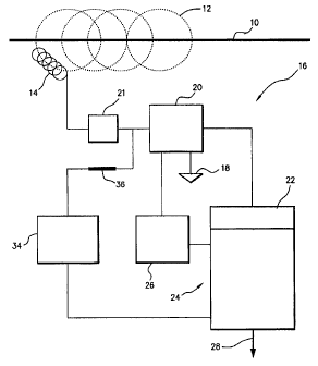
In Figure 1, an AC signal in a power line 10 generates
a magnetic field 12 around the power line 10. A conductive
coil 14 of the device 10 is placed in the vicinity of the
power line 10 in a manner such that at least a portion of
the magnetic field lines of the magnetic field 12 passes
through the loops of the coil 14, thereby inducing an AC
signal in the coil 14, which is connected to an internal
ground 18 of the device 16 through an analogue
amplification stage 20. An integrator 21 is provided
before the amplification stage 20. In the analogue
amplification stage 20, the AC voltage across the coil 14
is amplified and the amplified AC voltage signal is
inputted into an analogue to digital converter 22 of a
microcontroller 24.
The microcontroller 24 controls a gain control unit 26
which in turn controls the gain of the analogue
amplification stage 20. When the microcontroller 24
detects that the amplitude of the converted AC voltage
signal has reached a predetermined value, it generates a
control signal to the gain control unit 26, in response to
which the gain control unit 26 reduces the gain of the
amplification stage 20. Thereby, saturation of the
amplification stage 20 can be avoided and measurements can
continue for higher AC voltage signals from the coil 14.
In the microcontroller 24, the converted AC voltage
signal is correlated with the control signals sent to the
gain control unit 26, and the control unit 24 generates an
output signal 28 which is representative of waveform, which
includes the amplitude, phase and harmonic content of the
AC voltage signal in the coil 14, which is a measure for
the alternating current signal in the power line 10.
In Figures 2a to c, the output signal 28, the
amplified voltage signal 30 and the amplitude of an AC
signal 32 in the power line 10 are illustrated.
WO 00/62084 CA 02366531 2001-10-10 PCT/AUOO/00315
- 10 -
Referring again to Figure 1, the device 16 further
comprises an offset compensation unit 34. The offset
compensation unit 34 receives a digital signal from the
micro controller 24 representative of a DC component in the
amplified AC voltage signal. The offset compensation unit
34 outputs a DC trimming signal which is added through a
resistor 36 to the integrated AC voltage signal across the
coil 14 at the input of the amplification stage 20.
Within the offset compensation unit 34, the amplitude
of the generated DC trimming signal is varied to maintain
the digital DC component signal received from the
microcontroller 24 at a minimum. This can allow the
amplification stage 20 to be operated at high gains without
loss of performance caused by amplification of DC offset
voltages.
Turning now to Figure 3, the input signal 100 and an
offset correction signal 110 are added through resistor
120. This signal is applied to the non-inverting input of
operational amplifier 130. The DC gain of amplifier 130 is
R2
equal to G=1+ -,where Rinis the input resistance between
Rin
the inverting input of the amplifier and the reference
voltage for the amplifier (VCC/2). Device 140 is a
digitally controlled analog switch that is chosen to have
an "off" resistance much higher than the resistor labelled
R2/63. Similarly, the "on" resistance of the analog switch
is chosen to be much less than the resistor labelled R2/63.
Thus, when a control signal from the microcontroller 150 is
activated, 140 is switched "ON", its resistance is low, so
the DC gain of the amplifier 130 is given by
R2
G,:t~ l+ _
R2/63 1+63=64. When device 140 is switched "OFF",
its resistance is high, so the DC gain of the amplifier is
R2 '
given by Gz:~1+-= 1+ 0= 1. Thus, the activation siinal from
00
WO 00/62084 CA 02366531 2001-10-10 PCT/AUOO/00315
- 11 -
the microcontroller 150 is used to set the DC gain of the
amplifier 130 to either 64 or 1. Capacitor Cl is a small
value device and is used to filter out ringing in the
output signal following a gain change.
Amplifier 160 amplifies the signal from amplifier 130
and has gains set by R3, R3/3, R3/15, switch 170, and
switch 180. The gains of this stage are shown below:
Signal Signal Gain of
labelled labelled Amplifier 160
B1G16 B1G4
0 0 1
0 1 4
1 0 16
By combining the gains of amplifiers 130 and 160, the
following gain settings are possible:
Signal Signal Signal Gain (total)
labelled labelled labelled
B1G64 B1G16 B1G4
0 0 0 1
0 0 1 4
0 1 0 16
1 0 0 64
1 0 1 256
1 1 0 1024
The resistor R4 and capacitor C3 are used to lowpass
filter the signal prior to the analog to digital converter
in the microcontroller.
Turning now to Figure 4, the circuitry described below
provides a technique to digitally correct for offset
voltage in low cost, low power operational amplifiers.
This allows the amplifiers to be operated at high gains
without loss of performance caused by amplification of
offset voltages.
CA 02366531 2009-03-26
- 12 -
Circuit Operation:
Devices 200 and 210 are serial to parallel shift
registers. The most significant bit of shift register 200
is named D7 and is connected to the input of shift register
210. This gives a twelve digital output DO-Dil. The
inputs to the shift register (200 + 210) are generated by
the microcontroller and are labelled DACDATA and DACCLK.
These outputs are connected to the R-2R resistor network
220 to form a digital to analog converter. The output
range of this analog to digital converter is from zero to
(4095/4096)(SHIFTVCC), when SHIFTVCC is a predetermined DC
signal. The output of the digital to analog converter is
attenuated by resistor R1 and R2 and added to voltage VCC/2
to give a small voltage that varies around VCC/2. This
voltage is filtered by Cl and buffered by buffer 230 to
give signal BITRIM.
The trimming software functions by setting the
amplifier circuit shown in Figure 3 to maximum gain. In
the presence of a low input signal, the value of BITRIM
that minimises the DC offset voltage seen by the
microcontroller 150 is obtained using a binary search
technique.
Returning now to Figure 1, the microcontroller 24 also
performs an analysis of the frequency components of the
amplified AC voltage signal, and thus of the frequency
components of the magnetic field 12.
A lowpass filter is used to provide a signal
proportional to the amplitude of the mains frequency
component of the magnetic field (M1). A bandpass filter is
used to provide a signal proportional to the second
harmonic component of the magnetic field (MZ). If the
ratio of MZ / M1 exceeds a predetermined ratio, then the
magnetic field signal is determined to be caused by
magnetising inrush current.
In Figure 5, in another embodiment a device 300
WO 00/62084 CA 02366531 2001-10-10 PCT/AUOO/00315
- 13 -
further comprises a capacitor arrangement 310 for measuring
the electric field generated by the AC voltage signal on
the power line 10. Both the signal from the capacitor
arrangement 310 and the coil arrangement 330 are processed
substantially as described before for the embodiment
incorporating only a coil for the measurement of magnetic
fields. Similarly as for the magnetic field measurements,
this results in an electric field measurement in which a
value representing a parameter of the electric field can be
determined on a "continuous" scale.
The device 300 allows the detection of a common but
elusive type of fault, commonly called self-clearing fault.
These faults are characterised by high levels of current
but do not cause a trip. By measuring an increase or
decrease in the magnitude of the electric field,
accompanied by changes in the current, self-clearing faults
may be detected and stored.
The device 300 incorporating the capacitor arrangement
310 for measuring the electric field can also be used to
perform what is commonly referred to as a "distance to
fault calculation".
Referring now to Figure 6, the impedance of the line
between the supply and the fault indicator is dominated by
inductance LS and resistance R.
The impedance of the line between the fault indicator
and the fault is dominated by inductance LF and resistance
RF.
The impedance of the line and load beyond the fault
location is dominated by inductance LL and resistance RL.
During the fault, it is assumed that the voltage at
the fault is small compared to the supply voltage.
The voltage seen at the fault indicator is:
diF
VF = LFRF + LF dt 1.1
WO 00/62084 CA 02366531 2001-10-10 PCT/AUOO/00315
- 14 -
diF
where iFis the fault current and dt is the time
derivative of the fault current.
If the voltage at the fault indicator is measured when
iF is zero, then we have:
:
diI
V,: = LF dt ;F_o
Rearrangement gives
dt
L,.- = Vf diF iF-O 1.2
Thus, we may calculate the inductance of the line
between the fault indicator and the fault.
Now, the per/metre inductance of the line is a
constant that varies little with the configuration or
voltage of the line. Thus it is considered to be
approximately constant for all lines. We may write:
LF = k x d,
where k is the inductance per metre and d is the
length of the line in metres.
Similarly, we have:
d= Lk . 1.3
Combining (1.2) and (1.3) gives
dt
VF di iF-O
d= k 1.4
Equation (1.4) is the basis for the distance to fault
measurement technique. Note that this technique is used in
other products.
If several devices incorporating electrical field
measurements components are used, the distance to fault
reported by each indicator may be used to refine the search
for the location of the fault.
It will be appreciated by a person skilled ira the art
that numerous variations and/or modifications may:,rbe made
WO 00/62084 CA 02366531 2001-10-10 PCT/AUOO/00315
- 15 -
to the present invention as shown in the specific
embodiments without departing from the spirit or scope of
the invention as broadly described. The present
embodiments are, therefore, to be considered in all
respects to be illustrative and not restrictive.
For example, it will be appreciated that the present
invention is not limited to measurements performed on a
single conductor, but rather the measurements could be
conducted on a plurality of adjacent power lines. In such
circumstances, one or more sensors (such as coil 14 of
Figure 1) could be used.
For example, it will be appreciated that the
measurement may also be performed utilising two or more
coils with an angular offset between them to establish the
characteristics of the magnetic field.