Note: Descriptions are shown in the official language in which they were submitted.
CA 02366894 2002-O1-02
Patent-Treuhaad-C~esel l schaf t
fur elektrische C3l~ihlampen mbH. , Munich
Circuit arrangement for operating electric lamps
The invention relates to a circuit arrangement
according to the preamble of patent claim 1.
I. Prior Art
A circuit arrangement of this type is described, for
example, in the European publication EP 0 682 464 A1.
This publication discloses a self-oscillating inverter
having a starting circuit which is used to start the
inverter oscillating. In addition, the circuit
arrangement also has a device for deactivating the
starting circuit. This device contains, as an important
element, a transistor whose switching path, when
switched on, forms a shunt around the charging
capacitor of the starting circuit. After the inverter
has begun oscillating, the transistor is switched on
and the starting device is deactivated.
The European publication EP 0 753 987 A1 describes a
circuit arrangement having an inverter to apply a
medium or high-frequency supply voltage to one or more
lamps and having a starting circuit which is used to
start the inverter oscillation. In addition, this
circuit arrangement also has a device for deactivating
the starting circuit. This device comprises a resistor
and a diode, via which the capacitor of the starting
device is discharged after the inverter has begun to
oscillate, so that the starting device is not able to
produce any further triggering pulses to drive the
inverter. In the case of a lamp which is defective or
unwilling to fire, the inverter is stopped with the aid
of a bistable shutdown device. In order to reset the
bistable shutdown device and thus to permit the
inverter to be restarted, the voltage supply to the
CA 02366894 2002-O1-02
- 2 -
inverter or to the lamp must be interrupted, at least
briefly.
II. Summary of the invention
It is an object of the invention to provide a circuit
arrangement for operating electric lamps which is
improved as compared with the prior art.
According to the invention, this object is achieved by
the features of patent claim 1. Particularly
advantageous embodiments of the invention are described
in the dependent claims.
The circuit arrangement according to the invention has
an inverter for generating a medium or high-frequency
supply voltage for one or more lamps and a starting
circuit for the inverter, and also a device for
deactivating the starting circuit; the starting circuit
having a voltage-dependent switching means and a
capacitor. The device for deactivating the starting
circuit has a switching means whose switching path is
arranged in parallel with the capacitor of the starting
device. In order to control this switching means, the
device for deactivating the starting circuit according
to the invention is provided with a threshold switch.
By means of this measure, deactivation of the starting
circuit is ensured even when the inverter does not
begin to oscillate. In addition, by means of the
threshold switch, a time delay between the generation
of the first starting pulse by the starting circuit and
the deactivation of the starting circuit is made
possible. As a result of the measure according to the
invention, it is also possible for a simpler and more
cost-effective shutdown device to be used, in order to
shut down the inverter in the event of a defective
lamp.
In addition, the threshold switch is advantageously
CA 02366894 2002-O1-02
- 3 -
arranged in such a way, and the device for deactivating
the starting circuit is advantageously constructed in
such a way that, after the supply voltage for the
inverter has been switched on, the threshold switch is
activated with a time delay. with respect to the
starting circuit: This ensures that the starting
circuit is able to generate at least one or two trigger
pulses in order to start the inverter oscillating
before it is deactivated by means of the threshold
switch.
A further advantage of the circuit arrangement
according to the invention is that, instead of a
bistable shutdown device, a shutdown device constructed
as a threshold switch can be used, which is more cost-
effective and has a simpler construction. Although the
shutdown device constructed as a threshold switch is
not bistable and, in particular, is not able to ensure
a stable shutdown state without further measures, since
the device for deactivating the starting circuit has a
means which is used to maintain the deactivated state
of the starting circuit when the supply voltage for the
inverter is switched on and after the shutdown device
has responded, and the device for deactivating the
starting circuit interacts with the shutdown device
constructed as a threshold switch, the circuit
arrangement according to the invention ensures that
after the shutdown device has responded, the
oscillation of the inverter is terminated permanently,
and it is possible to restart the oscillation of the
inverter only after the supply voltage for the inverter
or for the lamp has been switched on again.
In order to implement the aforementioned time-delayed
deactivation of the starting circuit by means of the
threshold switch belonging to the device for
deactivating the starting circuit, the starting circuit
and the device for deactivating the starting circuit
advantageously have RC elements of different
CA 02366894 2002-O1-02
- 4 -
dimensions. The time constants of the two
aforementioned RC elements are coordinated with each
other in such a way that after the supply voltage for
the inverter has been switched on, the threshold
voltage of the trigger component of the starting device
is reached earlier than the threshold device of the
threshold switch belonging to the device for
deactivating the starting circuit. For this purpose,
the time constant of the RC element belonging to the
starting circuit is advantageously smaller than the
time constant of the RC element belonging to the device
for deactivating the starting circuit.
In order to achieve a sufficiently short reset period
for the device for deactivating the starting circuit, a
discharge resistor is advantageously arranged in
parallel with the RC element belonging to the device
for deactivating the starting circuit, and is used to
discharge the capacitor when the supply voltage for the
inverter is switched off. The discharge resistor and
the capacitor of the aforementioned RC element are
dimensioned such that the product of the resistance of
the resistor and the capacitance of the capacitor is
less than 500 ms and preferably even less than 100 ms .
As a result, the aforementioned capacitor is virtually
completely discharged after the oscillation of the
inverter has decayed.
As a central component, the device for deactivating the
starting device has a switching means which is
advantageously constructed as a transistor and whose
switching path is arranged in parallel with the
capacitor of the RC element belonging to the starting
circuit, the threshold switch belonging to the device
for deactivating the starting device being connected to
the control electrode of the transistor and to the
capacitor of the RC element belonging to the device for
deactivating the starting circuit. In the low-
resistance switching state, the switching path of this
CA 02366894 2002-O1-02
- 5 -
transistor forms a shunt to the capacitor of the
starting device and therefore ensures that the
capacitor belonging to the starting circuit is
discharged or prevents this capacitor being recharged.
The means already mentioned above which, when the
supply voltage for the inverter is switched on and
after the shutdown device has responded, is used to
maintain the deactivated state of the starting circuit,
advantageously comprises an electrical connection
between the voltage supply of the inverter and the
control electrode of the transistor, the aforementioned
electrical connection being routed via the threshold
switch belonging to the device for deactivating the
starting circuit. As a result, the transistor remains
in the switched-on state after the oscillation of the
inverter has been terminated by the shutdown device.
The starting circuit therefore remains in the
deactivated state.
In order to achieve the most immediate deactivation of
the starting circuit, after the oscillation of the
inverter has started, the control transformer of the
self-oscillating oscillator (or an additional winding
on a lamp inductor) is used, its primary winding being
arranged in a load circuit of the inverter and its
secondary winding being used to drive the control
electrode of the transistor belonging to the device for
deactivating the starting circuit. With the aid of the
transformer, the start of the inverter oscillation is
monitored and the aforementioned transistor is driven
appropriately.
III. Description of the preferred exemplary embodiment
The invention will be explained in more detail below
using a preferred exemplary embodiment. The figure
shows a schematic representation of a circuit diagram
of the preferred exemplary embodiment of the circuit
CA 02366894 2002-O1-02
- 6 -
arrangement according to the invention.
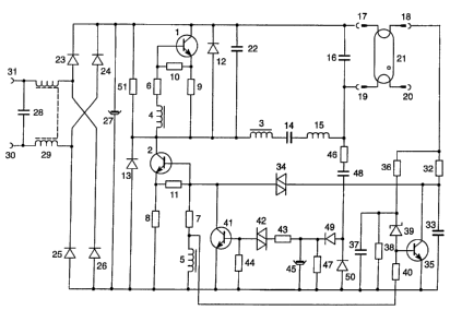
The circuit arrangement depicted in the figure is used
to operate a low-pressure discharge lamp with an
electrical power consumption of about 18 W. This
circuit arrangement has a self-oscillating half-bridge
inverter, which is substantially formed by the
alternately switching transistors 1, 2 and the
freewheeling diodes 12, 13 and the toroidal transformer
3-5. The toroidal transformer 3-5 is used to control
the transistors 1 and 2. For this purpose, the primary
winding 3 of the toroidal transformer is arranged in
the load circuit, constructed as a series resonant
circuit, of the half-bridge inverter, while the
secondary windings 4 and 5 are in each case connected
via a base bias resistor 6 and 7 to a base electrode of
a half-bridge inverter transistor 1 and 2. The control
device for the transistors 1 and 2 is completed by the
Knitter resistors 8 and 9, the resistors 10, 11 and the.
capacitor f2, which reduces the switching losses in the
transistors 1, 2. The load circuit is connected to the
center tap between the transistors 1, 2 of the half-
bridge inverter. In addition to the primary winding 3
of the toroidal transformer, it contains a coupling
capacitor 14, a resonance inductor 15 and a resonance
capacitor 16. The terminals 17-20 for the electrode
filaments of the low-pressure discharge lamp 21 are
arranged in such a way that the discharge path of the
low-pressure discharge lamp 21 is connected in parallel
with the resonance capacitor 16. The voltage supply to
the half-bridge inverter is provided by rectifying the
alternating mains voltage with the aid of a bridge
rectifier comprising four diodes 23-26 and a capacitor
27, which is arranged in parallel with the direct
current output from the bridge rectifier 23-26. A
smoothed DC voltage is therefore provided on the
capacitor 27 as a voltage supply for the half-bridge
inverter. The coupling capacitor 14 is charged up via
the resistor 51 after the voltage supply has been
CA 02366894 2002-O1-02
switched on. A filter circuit which comprises a
capacitor 28 and a current-compensated inductor 29 and
which is connected to the mains voltage connections 30,
31 and to the alternating current input of the bridge
rectifier 23-26 ~s used to suppress the radio
interference from the circuit arrangement. In addition,
the circuit arrangement has a starting device for the
half-bridge inverter, which substantially comprises the
resistor 32 and the capacitor 33 and the diac 34. The
starting circuit is used to initiate the oscillation of
the half-bridge inverter, by generating trigger pulses
for the base electrode of the transistor 2 after the
voltage supply for the half-bridge inverter has been
switched on.
The part described above of the circuit arrangement
according to the preferred exemplary embodiment is
known and, for example, described in the prior art
cited at the beginning. The construction and the
function of this part of the circuit arrangement are
therefore not to be explained in more detail here.
The circuit arrangement further has a device for
deactivating the starting circuit and a shutdown device
for stopping the half-bridge inverter in the event of a
defective lamp. The device for deactivating the
starting circuit comprises the transistor 35, whose
switching path is arranged in parallel with the
capacitor 33 of the starting circuit, the RC element
36, 37, which is connected in parallel with the RC
element 32, 33, the resistor 38, which is used to
discharge the capacitor 37 when the voltage supply is
switched off or interrupted,. the Zener diode 39, whose
cathode is connected on one side, via the resistor 36
and the terminals 17, 18, and via an electrode filament
of the lamp 21, to the positive terminal of the
capacitor 27 and on the other side to the terminal of
the capacitor 37 that is at higher potential, and whose
anode is connected to the base of the transistor 35,
CA 02366894 2002-O1-02
-
and also comprises the base bias resistor 40, via which
the base of the transistor 35 is connected to the
secondary winding 5 of the toroidal transformer.
The shutdown device for stopping the half-bridge
inverter is constructed as a threshold switch and
comprises the transistor 41, whose switching path is
connected in parallel with the series circuit
comprising the base bias resistor 7 of the transistor 2
and the secondary winding 5, the diac 42, which
generates trigger pulses for the base of the transistor
41 when it reaches its threshold voltage, the bias
resistors 43, 44, the capacitor 45, which is used for
the voltage supply of the diac 42 and the base of the
transistor 41, the voltage divider resistors 46, 47,
with the aid of which a voltage proportional to the
operating voltage of the lamp 21 is generated and with
the aid of which the threshold voltage for activating
the shutdown device is defined, the capacitor 48, which
serves to decouple the DC component in the lamp
current, and the rectifier diodes 49, 50 serving as
current valves.
Suitable dimensioning of the components of the circuit
arrangement is indicated in the table.
Immediately after the voltage supply has been switched
on, the coupling capacitor 14 is charged up via the
resistor 51, and the capacitor 33 of the starting
circuit is charged up via the resistor 32. As soon as
the voltage drop across the capacitor 33 has reached
the threshold voltage of the diac 34, the diac 34
generates trigger pulses for the base of the transistor
2. As a result, the oscillation of the half-bridge
inverter is triggered. The two transistors 1, 2 of the
half-bridge inverter switch alternately, so that a
medium or high-frequency current flows in the load
circuit. The frequency of this current is determined by
the switching frequency of the transistors 1, 2. Since
CA 02366894 2002-O1-02
_ g -
the load circuit is constructed as a series resonant
circuit, the firing voltage required to fire the gas
discharge in the lamp 21 can be provided on the
resonance capacitor 16 by the resonant peak method.
After the gas discharge has been fired, the capacitor
16 is short-circuited by the discharge path of the low-
pressure discharge lamp 21, which is then conductive.
The starting circuit is deactivated immediately after
the half-bridge inverter begins to oscillate, by means
of the primary winding 3 connected into the load
circuit and the secondary winding 5 of the toroidal
transformer. As soon as the half-bridge inverter has
begun its oscillation, a medium or high-frequency
current flows in the load circuit and, in particular,
through the primary winding 3, and induces in the
secondary winding 5 a corresponding voltage for
controlling the bases of the transistors 2 and 35. The
transistor 35 is therefore switched on via its base
bias resistor 40 and, as a result, the capacitor 33 is
able to discharge via the transistor 35, so that the
threshold voltage of the diac 34 is no longer reached
and the diac 34 does not produce any further trigger
pulses. Because it is driven by the transformer
windings 3, 5, the transistor 35 switches in the same
rhythm as the transistor 2. However, the capacitor 33
is not charged up to a noticeable extent as a result.
As has already been disclosed above, the base of the
transistor 35 is additionally also driven via the RC
element 36, 37 and the Zener diode 39. The capacitor 37
is charged up via the resistor 36 at the same time as
the capacitor 33 after the voltage supply has been
switched on. Since the time constant of the RC element
36, 37 is greater than the time constant of the RC
element 32, 33 of the starting circuit, however, the
threshold voltage required for switching on the diac 34
is provided earlier on the capacitor 33 than the
threshold voltage required on the capacitor 37 to
CA 02366894 2002-O1-02
- 10 -
switch on the Zener diode 39. The diac 34 is therefore
able to generate at least one or two trigger pulses for
controlling the base of the transistor 2 before the
capacitor 37 is charged up to the threshold voltage of
the Zener diode 39 and the transistor 35 which is
switched on via the Zener diode 39. For the case in
which the oscillation of the half-bridge inverter
cannot be started by means of the trigger pulses from
the diac 34, and therefore control of the transistor 35
by means of the transformer windings 3, 5 is not
possible, the transistor 35 is switched on via the
Zener diode 39 after the capacitor 37 has been charged
up to the threshold voltage of the Zener diode 39, and
the capacitor 33 of the starting circuit is discharged
via the transistor 35. The starting circuit will
therefore be deactivated in any case. After the
transistor 35 has been switched on via the Zener diode
39, the transistor 35 remains in the switched-on state,
even after the voltage on the capacitor 37 has fallen
below the threshold voltage of the Zener diode 39 since
the Zener diode 39 is connected to the electrolytic
capacitor 27 via the current path which contains the
components 5, 40, 39, 36 and the terminals 17, 18 and
also the electrode filament of the lamp 21 connected
thereto, and, as a result, the on state of the Zener
diode 39 is maintained. Only by means of the voltage
supply to the circuit arrangement or to the half-bridge
inverter being switched on again, or by means of a
brief interruption to the aforementioned current path,
for example by replacing the lamp 21, can the
transistor 35 be turned off and the starting circuit be
activated again.
The function of the shutdown device and its interaction
with the device for deactivating the starting circuit
will be explained in more detail below.
The shutdown device monitors the positive half wave of
the alternating voltage component of the operating
CA 02366894 2002-O1-02
- 11 -
voltage of the low-pressure discharge lamp 21 by means
of the voltage divider resistors 46, 47 and the
capacitor 48 and also the rectifier diode 49. The
capacitor 48 is conductive only to the alternating
voltage component of the lamp operating voltage. The
negative half wave of this alternating voltage
component is clamped to ground by the diode 50. A
voltage that is proportional to the positive half wave
of the alternating voltage component of the lamp
operating voltage is present across the resistor 47.
The capacitor 45 is also charged up to the same voltage
value . For the case of a lamp 21 which is defective or
does not wish to fire, or for the case where the
operating voltage of the lamp 21 has grown excessively
as a result of aging, the voltage drop across the
capacitor 45 reaches the threshold voltage of the diac
42. The diac 42 then generates trigger pulses for the
base of the transistor 41. As a result, the transistor
41 is switched on via the resistor 43 , the disc 42 and
the base bias resistor 44, and withdraws the control
signal from the base of the transistor 2, so that the
oscillation of the half-bridge inverter is terminated.
The transistor 41 remains switched on only until the
capacitor 45 has discharged to such an extent that the
voltage drop across the capacitor 45 is less than the
threshold voltage of the diac 42. The transistor 41
then returns into the blocked state. Since the starting
circuit is deactivated by discharging the capacitor 33
via the switched-on transistor 35, the diac 34 is not
able to generate any trigger pulses to start the half-
bridge inverter oscillating again. The half-bridge
inverter is therefore stopped permanently, although the
control signal was withdrawn from the base of the
transistor 2 only for a relatively short time interval.
In order to permit the half-bridge inverter to begin to
oscillate again, the starting circuit must first be
reactivated by resetting the transistor 35 into the
blocked state. This may be achieved by means of a brief
interruption to the voltage supply to the circuit
CA 02366894 2002-O1-02
- 12 -
arrangement or by replacing the lamp 21.
Following the interruption of the voltage supply, the
period until the oscillation of the half-bridge
inverter decays is about 0.5 s to 1 s. The two
components 37, 38 are dimensioned such that the
capacitor 37 is virtually completely discharged at the
end of the oscillation of the half-bridge inverter.
The invention is not restricted to the exemplary
embodiment explained in more detail above.
The circuit arrangement according to the invention can,
for example, additionally have a temperature
compensation element, which is used to adapt the
shutdown threshold of the shutdown device to the
temperature-dependent burning voltage of the lamp 21.
It has been shown that the operating voltage of the
lamp can decrease as the temperature increases. In
order to adapt the shutdown threshold of the shutdown
device accordingly, a temperature compensation element
is provided which comprises the appropriately
dimensioned parallel circuit comprising a non-reactive
resistor and an NTC resistor. This parallel circuit can
be integrated into the circuit arrangement according to
the invention, for example at the junction which is
defined by the components 48, 49, 50.
In addition, a PTC resistor, for example, can be
arranged between the terminals 18 and 20 of the circuit
arrangement according to the invention, in order to
permit preheating of the electrode filaments in the
lamp 21 before the gas discharge therein is fired.
Furthermore, the circuit arrangement according to the
invention can additionally have a harmonic filter
according to European patent EP 0 244 644, in order to
ensure a sinusoidal mains current consumption. In this
case, the shutdown device can also monitor the voltage
CA 02366894 2002-O1-02
- 13 -
drop across the capacitor 27, in addition to the lamp
operating voltage, for example by the positive terminal
of the capacitor 27 being connected, via a Zener diode
polarized in the reverse direction, to the junction
defined by the components 43, 45 and 49.
The circuit arrangement according to the invention can
additionally also be constructed in such a way that it
is suitable for the operation of a plurality of low-
pressure discharge lamps connected in series or
parallel. The shutdown device according to the
invention can in addition also be used in circuit
arrangements for operating high-pressure discharge
lamps or incandescent halogen lamps.
CA 02366894 2002-O1-02
_ ~y .~.
Table Dimensioning of the electrical components
according to the preferred exemplary embodiment
1, 2 BUJ105A
3, 4, 5 7/2/2 windings
6; 7 6.8 52
8 , 9 0 . 4 7 52
10, 11 33 SZ
12, 13 BYD33J
14, 28 220 nF
15 1.5 mH
16 10 nF
22 3.3 nF
23-26 1N4007
27 4.7 ~,F
29 2x39 mH
3 2 1. 2 MS2
33, 37 100 nF
35 BC847A
36, 51 2 MS2
38, 44, 47 220 kSZ
40 68 kS2
41 BC368
43 100SZ
45 22 ~.F
46 470 kS2
48 2.2 nF
49, 50 1N4148