Note: Descriptions are shown in the official language in which they were submitted.
CA 02367166 2002-O1-10
Doc. No. 10-370 CA Patent
SEGMENTED OPTICAL SWITCH
The present invention relates to an optical switch, and in particular to a
segmented
M x N optical switch.
BACKGROUND OF THE INVENTION
In the fiber optics industry M x N optical switches are used to selectively
optically
couple one of a plurality of input optical fibers with one of a plurality of
output optical
fibers. United States Patent No. 4,580,873, issued April 8, 1986 to Frank
Levinson,
discloses a basic M x N optical switch having an array of input lenses along
one side and
an array of output lenses along another side.
As the demand for the transmission of greater amounts of information grows, so
does the number of optical fibers, and so does the size of the switches, which
are required
to direct the beams of light carrying the information. However, there are
definite
physical limits within which the design of a switch must adhere. Basic
economics dictate
that the switch should be as small as possible to minimize material costs, but
there are
several other interrelated factors that play a role in the design of a switch.
These factors
include lens characteristics, mirror size, and optical path length. A Gaussian
beam
launched through an appropriate lens initially converges and subsequently
diverges. The
minimum beam diameter is called the waste, the position and size of which are
based on
the parameters of the lens and the beam. The position of the waist is
important since the
beam diameter increases thereafter, and it is the diameter of the beam that
dictates the
size of the mirrors and the maximum optical path length to ensure good optical
coupling.
When all of the lenses have the same focal length, insertion loss is minimized
by making
the distance from the collimating lens to the reflecting mirror the same as
the distance
from the reflecting mirror to the focusing lens, and by focussing the beam
waist on the
reflecting mirror. Obviously, this is impossible for every combination of
input and
output lens. Accordingly, to minimize the variation in insertion loss, it is
important to
minimize the variation in the optical path lengths and to position the beam
waist at the
average optical path length. However, in the conventional matrix switch, the
optical path
length from the first input port to the first output port is short, while the
optical path
CA 02367166 2002-O1-10
Doc. No. 10-370 CA Patent
length from the last input port to the last output port is much longer.
Therefore, when
conventional switches are used with a large number of input/output ports the
variation in
optical path lengths is very large, resulting in a large variation in
insertion loss.
A previous attempt to equalize all of the path lengths is disclosed in United
States
Patent No. 5,841,917, issued November 24, 1998 to Jungerman, Roger L. et al.
Unfortunately, the arrangement disclosed in the Jungerman et al patent is
quite bulky and
cumbersome, particularly as the number of input/output ports increases.
An object of the present invention is to overcome the shortcomings of the
prior art
by providing an optical switch with a minimum insertion loss variation by
minimizing the
variation in optical path lengths.
SUMMARY OF THE INVENTION
Accordingly, the present invention relates to a segmented optical switch
comprising:
a first segment including P input ports for launching beams of light into the
switch;
a second segment, adjacent the first segment, including X output ports for
receiving
beams of light from the switch;
a third segment, adjacent the second segment, including Q input ports for
launching
beams of light into the switch; and
a fourth segment, adjacent the first and third segments, including Y output
ports for
receiving beams of light from the switch;
wherein the first segment also includes P x Y reflecting means for redirecting
the beams
of light from the P input ports to the Y output ports;
wherein the second segment also includes P x X reflecting means for
redirecting the
beams of light from the P input ports to the X output ports;
wherein the third segment also includes Q x X reflecting means for redirecting
the beams
of light from the Q input ports to the X output ports; and
wherein the fourth segment also includes Q x Y reflecting means for
redirecting the
beams of light from the Q input ports to the Y output ports.
CA 02367166 2002-O1-10
Doc. No. 10-370 CA Patent
BRIEF DESCRIPTION OF THE DRAWINGS
The present invention will be described in greater detail with reference to
the
accompanying drawings which illustrate a preferred embodiment of the invention
and
wherein:
Figure 1 is a schematic plan view of a convention 16 x 16 optical switch;
Figure 2 is a schematic plan view of a segmented 16 x 16 optical switch
according
to the present invention;
Figure 3 is a plot of the insertion loss for the various input/output port
combinations for a conventional 16 x 16 switch and for the segmented 16 x 16
optical
switch according to the present invention;
Figure 4 is a schematic plan view of a second embodiment of an optical switch
according to the present invention; and
Figure 5 is a schematic plan view of a third embodiment of an optical switch
according to the present invention.
DETAILED DESCRIPTION
Figure 1 illustrates a conventional 16 x 16 optical switch 1 including sixteen
input
ports 2a to 2p, and sixteen output ports 3a to3p. Each input port 2a to 2p
includes a
collimating lens 4 receiving input fibers 5, and each output port 3a to 3p
includes a
focusing lens 6 receiving output fibers 7. The switch 1 also includes a 16 x
16 array of
reflective minors 8, aligned between the input ports 2a to 2p and the output
ports 3a to
3p. The mirrors 8 are mounted on a substrate 9 and selectively positioned in
the path of
an input beam of light to direct the beam at any one the output ports 3a to
3p. In the
illustrated example, the optical path length from input port 2a to output port
3a would be
very short, while the optical path length from input port 2p to output port 3p
is much
longer. Accordingly, the insertion loss would be large for both of these
examples, if the
lenses 4 and 6 are designed for the average optical path length defined by
input port 2i to
output port 2i. The plot for the unsegmented switch in Figure 3 illustrates
the variation in
the insertion losses, between the various path lengths in a conventional
switch.
CA 02367166 2002-O1-10
Doc. No. 10-370 CA Patent
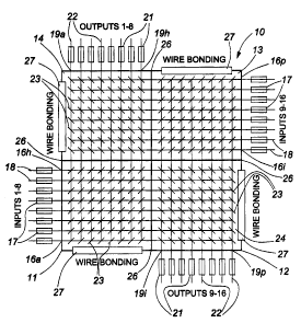
The large variation in the insertion loss is eliminated by the use of a switch
designed according to the present invention, an embodiment of which is
illustrated in
Figure 2. The illustrated switch, generally indicated at 10, includes four
segments 11, 12,
13 and 14. The first and third segments 11 and 13, respectively, include input
ports 16a
to 16p. The first and third segments 11 and 13, respectively, can include any
number of
ports, although it is preferable that the first segment 11 includes the same
number of ports
as the third segment 13, i.e. the input ports are equally divided between the
two segments.
Each input port 16a to 16p includes a collimating lens 17 receiving an input
optical fiber
18. The second and fourth segments 12 and 14, respectively, include output
ports 19a to
19p. The second and fourth segments 12 and 14, respectively, can include any
number of
ports, although it is preferable that the ports 19 be equally distributed
between the two
segments 12 and 14. Each output port 19a to 19p includes a focusing lens 21,
which
receives an output optical fiber 22. Preferably, both the collimating lenses
17 and the
focusing lenses 21 are approximately t/s pitch graded index (GRIN) lenses.
For the sake of convenience, the ports 16a to 16p are referred to as input
ports
and the lenses 17 are referred to as collimating lenses, while ports 19a to
19p are referred
to as output ports and the lenses 21 are referred to as focusing lenses. In
practice, ports
I6a to 16p and 19a to 19p can be used as both input and output ports, i.e.
lenses 17 an 21
can be used as both collimating and focusing lenses.
Each segment 11 to 14 includes an 8 x 8 array of reflecting mirrors 23.
Preferably, the mirrors 23 are pivotally mounted on a microelectronic
substrate 24 using a
micro-electromechanical-type system (MEMS). However, any form of mirror system
is
acceptable, e.g. rotateably, horizontally or vertically moveable. It is
possible to construct
the entire switch using a single microelectronic substrate, however, due to
the segmented
nature of the switch, it is also possible to construct each segment
separately. The
individual segments could then be fixed together along connection lines 26. In
the
example illustrated in Figure 2, the switch 1 is constructed out of four
identical segments.
This would greatly decrease manufacturing costs, since it is much easier and
cheaper to
construct several identical segments rather than segments with various sizes
or one large
substrate. Each segment I 1 to 14 also includes a wire bonding 27 for
connecting power
to the various mirrors 23.
4
CA 02367166 2002-O1-10
Doc. No. t0-370 CA Patent
In use, the mirrors 23 of the first segment 11 are used to redirect the
optical
signals, entering input ports 16a to 16h, bound for output ports 19a to 19h.
Optical
signals entering input ports 16a to 16h destined for output ports 19i to 19p
are redirected
using the mirrors 23 of the second segment 12, while the appropriate mirrors
on the first
segment 11 are positioned out of the optical path thereof. Similarly, mirrors
23 on the
third segment 13 redirect optical signals entering input ports 16i to 16p,
bound for output
ports 19i to 19p. Furthermore, mirrors 23 of the fourth segment 14 redirect
optical
signals launched through input ports 16i to 16p destined for output ports 19a
to 19h.
The arrangement according to the present invention limits the variation in
insertion loss by narrowing the range of possible optical path lengths. For
example, in
the switch 10, the shortest optical path length would be from input port 16h
to output port
19a, while the longest optical path length would be from input port 16a to
output port
19h. Assuming that all of the lenses 17 and 21 are the same, the variance in
optical path
lengths would be similar to that of a switch having half the number of inputs
and outputs.
To further minimize the insertion losses, the lenses 17 are selected so that
they
focus the waists of the input beams at a mid-way point of the average optical
path length,
i.e. the lenses 17 of segment 11 focus the waists on the connection line 26
between first
and second segments 11 and l2,respectively, and the lenses 17 of segment 13
focus the
waists of input beams on the connection line 26 between the third and fourth
segments 13
and 14.
The "segmented plot" in Figure 3 illustrates much smaller insertion losses for
a
16 x 16 switch according to the present invention compared with the insertion
losses for a
conventional "unsegmented" 16 x 16 switch. This difference is not just based
on
reducing the overall optical path lengths, but on reducing the variance in the
optical path
lengths, i.e. eliminating the long and the short optical path lengths.
Figures 4 and 5 illustrate alternate embodiments of the switch of the present
invention comprising four segments, which are not all identical. Switch 30 of
Figure 4
has all the same elements as switch 10, but includes only 8 input ports 16a to
16h, equally
divided between first and third segments 11 and 13. In this case, the first
segment 11 is
identical to the third segment 13, and the second segment 12 is identical to
the fourth
segment 14. Each segment includes a 4 x 8 array of mirrors 23.
CA 02367166 2002-O1-10
Doc. No. 10-370 CA Patent
Similarly, switch 40 of Figure 5 includes all the same elements as switches 10
and
30, except that the input ports 16a to 161 are not equally divided between
first and third
segments 11 and 13, and output ports 19a to 191 are not equally divided
between second
and fourth segments 12 and 14. Consequently, the first segment 11 includes a 4
x 8 array
of mirrors 23, the second segment 12 includes a 4 x 4 array of mirrors 23, the
third
segment 13 includes a 8 x 4 array of mirrors 23, and the fourth segment 14
includes a 8 x
8 array of minors 23.
The switches 30 and 40 do not represent an optimum construction, since the
variance in optical path lengths has not been minimized. Moreover, the switch
can not be
manufactured out of four identical segments. However, any segmentation
according to
the present invention will reduce the variance in the optical path lengths,
and accordingly
the insertion loss.
6