Note: Descriptions are shown in the official language in which they were submitted.
CA 02367686 2001-09-10
WO 00/59047 PCTIUSOO/05975
HYBRID THERMIONIC ENERGY CONVERTER AND METHOD
FIELD OF THE INVENTION
This invention relates to the conversion of thermal energy to electrical
energy,
and electrical energy to refrigeration, and more particularly to a thermionic
converter
of improved efficiency and power densities, which utilizes electron tunneling
and
thermionic emission facilitated by the reduction in the barrier height from
image force
effects:
BACKGROUND OF THE INVENTION
The present invention was developed to fill a need for a device which
efficiently converts thermal energy to electrical energy at relatively low
operating
temperatures and with power densities large enough for commercial
applications. The
present invention also operates in reverse mode to provide efficient cooling.
Thermionic energy conversion is a method of converting heat energy directly
into electrical energy by thermionic emission. In this process, electrons are
thermionically emitted from the surface of a metal by heating the metal and
imparting
sufficient energy to a portion of the electrons to overcome retarding forces
at the
surface of the metal in order to escape. Unlike most other conventional
methods of
generating electrical energy, thermionic conversion does not require either an
intermediate form of energy or a working fluid, other than electrical charges,
in order
to change heat into electricity.
In its most elementary form, a conventional thermionic energy converter
consists of one electrode connected to a heat source, a second electrode
connected to a
heat sink and separated from the first electrode by an intervening space,
leads
connecting the electrodes to the electrical load, and an enclosure. The space
in the
enclosure is either highly evacuated or filled with a suitable rarefied vapor,
such as
cesium.
The essential process in a conventional thermionic converter is as follows.
The heat source supplies heat at a sufficiently high temperature to one
electrode, the
emitter, from which electrons are thermionically evaporated into the evacuated
or
CA 02367686 2001-09-10
WO 00/59047 PCT/USOO/05975
2
rarefied-vapor-filled interelectrode space. The electrons move through this
space
toward the other electrode, the collector, which is kept at a low temperature
near that
of the heat sink. There the electrons condense and return to the hot electrode
via the
electrical leads and the electrical load connected between the emitter and the
collector.
The flow of electrons through the electrical load is sustained by the
temperature difference between the electrodes. Thus, electrical work is
delivered to
the load.
Thermionic energy conversion is based on the concept that a low electron
work function cathode in contact with a heat source will emit electrons. These
electrons are absorbed by a cold, high work function anode, and they can flow
back to
the cathode through an external load where they perform useful work. Practical
thermionic generators are limited by the work function of available metals or
other
materials that are used for the cathodes. Another important limitation is the
space
charge effect. The presence of charged electrons in the space between the
cathode and
anode will create an extra potential barrier which reduces the thermionic
current.
Typical conventional thermionic emitters are operated at temperatures ranging
from 1400 to 2200K and collectors at temperatures ranging from 500 to 1200K.
Under optimum conditions of operation, overall efficiencies of energy
conversion
range from 5 to 40%, electrical power densities are of the order of 1 to 100
watts/cm2,
and current densities are of the order of 5 to 100 A/cm2. In general, the
higher the
emitter temperature, the higher the efficiency and the power and current
densities with
designs accounting for radiation losses. The voltage at which the power is
delivered
from one unit of a typical converter is 0.3 to 1.2 volts, i.e., about the same
as that of an
ordinary electrolytic cell. Thermionic systems with a high power rating
frequently
consist of many thermionic converter units connected electrically in series.
Each
thermionic converter unit is typically rated at 10 to 500 watts.
The high-temperature attributes of thermionic converters are advantageous for
certain applications, but they are restrictive for others because the required
emitter
temperatures are generally beyond the practical capability of many
conventional heat
sources. In contrast, typical thermoelectric converters are operable at heat
source
temperatures ranging from 500 to 1500K. However, even under optimum
conditions,
CA 02367686 2001-09-10
WO 00/59047 PCT/US00/05975
3
overall efficiencies of thermoelectric energy converters only range from 3 to
10%,
electrical power densities are normally less than a few watts/cm2, and current
densities
are of the order of 1 to 100 A/cm2.
From a physics standpoint, thermoelectric devices are similar to thermionic
devices. In both cases a temperature gradient is placed upon a metal or
semiconductor, and both cases are based upon the concept that electron motion
is
electricity. However, the electron motion also carries energy. A forced
current
transports energy for both thermionic and thermoelectric devices. The main
difference between thermoelectric and thermionic devices is whether the
current flow
is diffusive (thermoelectric) or ballistic (thermionic). A thermionic device
has a
relatively high efficiency if the electrons ballistically go over and across
the barrier.
For a thermionic device all of the kinetic energy is carried from one
electrode to the
other. The motion of electrons in a thermoelectric device is quasi-equilibrium
and
diffusive, and can be described in terms of a Seebeck coefficient, which is an
equilibrium parameter.
In structures with narrow barriers, the electrons will not travel far enough
to
suffer collisions as they cross the barrier. Under these circumstances, the
thermionic
emission theory is a more accurate representation of the current transport.
The current
density is given by:
j = AoT 2e kT , where A0 is the Richardson's constant, V is the barrier height
(electron work function), e is the electron charge, xis Boltzmann's constant,
and T is
the temperature. Richardson's constant A0 is given by A00 = (em xT2)/(27 h2),
where
m is the effective electron mass and h is Plank's constant.
The diffusion theory is appropriate for barriers in which the barrier
thickness
(length) is greater than the electron mean-free-path in one dimension, while
the
thermionic emission theory is appropriate for barriers for which the barrier
thickness
(length) is less than the mean-free-path. However, if the barrier becomes very
narrow,
current transport by quantum-mechanical tunneling becomes more prominent.
CA 02367686 2001-09-10
WO 00/59047 PCTIUSOO/05975
4
There remains a need to provide a more satisfactory solution to converting
thermal energy to electrical energy at lower temperature regimes with high
efficiencies
and high power densities.
SUMMARY OF THE INVENTION
The present invention seeks to resolve a number of the problems which have
been experienced in the background art, as identified above. More
specifically, the
apparatus and method of this invention constitute an important advance in the
art of
thermionic power conversion, as evidenced by the following objects and
advantages
realized by the invention over the background art.
An object of the present invention is to generate high power densities and
efficiencies of a typical thermionic converter, but to operate at temperature
regimes of
typical thermoelectric devices.
Another object of the present invention is to maintain thermal separation
between the emitter and collector.
A further object of the present invention is to minimize the effects of
thermal
expansion.
Additional objects and advantages of the invention will be apparent from the
description which follows, or may be learned by the practice of the invention.
Briefly summarized, the foregoing and other objects are achieved by an
apparatus which comprises: an electrically and thermally conductive electron
emitter;
an electrically and thermally conductive electron collector for receiving
electrons from
the emitter; a solid-state barrier disposed between and in intimate contact
with said
emitter and collector for filtering high energy electrons transferred from the
emitter to
the collector; one or more electrically and thermally conductive fractional
surface
contacts disposed between and in intimate contact with the emitter and
barrier, or the
barrier and collector, or a combination thereof; a thermally and electrically
nonconductive space adjacent to the fractional surface contacts and the
emitter and
barrier, or the barrier and collector, or a combination thereof; and an
electric load
connected to the emitter and collector.
CA 02367686 2001-09-10
WO 00/59047 PCT/US00/05975
In the refrigeration embodiment, carrier transport is assisted by a potential
applied between the emitter and collector, and the emitter is connected to a
thermal
load that is cooled by heat flow to the emitter. A heat exchanger dissipates
the heat
from hot electrons on the collector.
5
BRIEF DESCRIPTION OF DRAWINGS
In order to more fully understand the manner in which the above-recited
advantages and objects of the invention are obtained, a more particular
description of
the invention will be rendered by reference to specific embodiments thereof
which are
illustrated in the appended drawings. Understanding that these drawings depict
only
typical embodiments of the invention and are therefore not to be considered
limiting
of its scope, the presently preferred embodiments and the presently understood
best
mode of the invention will be described with additional detail through use of
the
accompanying drawings in which:
FIG. 1 is a cross-sectional view of a thermionic converter of the present
invention.
FIG. 2 illustrates a cross-sectional view of a fractional surface contact
having a
triangular cross-section.
FIG. 3 shows a perspective view of an emitter utilizing tantalum-hydride
powder with a honeycomb structure to support the powder.
FIGS. 4A and 4B shows a cross-sectional view of a low thermal conductivity
semiconductor barrier placed in a vacuum between a metal emitter and a metal
collector.
FIG. 5 illustrates a plot of Richardson thermionic current density versus
barrier
height at various temperatures.
FIG. 6 illustrates the thermal expansion pattern and nanowire positioning for
a
circular plate.
FIG. 7 illustrates the thermal expansion pattern and nanowire positioning for
a
rectangular plate.
FIG. 8 illustrates various nanowire cross-sections.
CA 02367686 2001-09-10
WO 00/59047 PCT/USOO/05975
6
FIG. 9 is a cross-sectional view of an embodiment of the present invention
wherein the fractional surface contact is associated with the barrier.
FIG. 10 is a cross-sectional view of a barrier configuration comprising a
metallic layer, an n-type semiconductor layer, a p-type semiconductor layer,
and a
metallic layer.
FIG. 11 is a cross-sectional view of a barrier configuration comprising a
metallic layer, an n-type semiconductor layer, and a metallic layer.
FIG. 12 is a cross-sectional view.of a barrier configuration comprising a
metallic layer, a p-type semiconductor layer, and a metallic layer.
FIG. 13 is a cross-sectional view of a barrier configuration comprising a
resonant tunneling diode.
FIG. 14 shows the transmission probability for a specific GaAs-Al,,Ga,_7zAs
heterostructure.
FIG. 15A shows a cross-sectional view of a nonmetallic collector with a
metallic layer.
FIG. 15B shows a cross-sectional view of a nonmetallic collector with a
metallic layer and a surface barrier matching material disposed between the
collector
and the barrier to prevent the leak back of electrons to the emitter.
FIG. 16 is an I-V curve for an emitter comprising TaH and a barrier
comprising A1,03.
FIG. 17 is an I-V curve for an emitter comprising TaH and a barrier
comprising A1203 at a different temperature differential than FIG. 16.
FIG. 18 is a plot of the voltage dependence on the temperature gradient for an
emitter comprising TaH and a barrier comprising A1203.
FIG. 19 is an I-V curve for an emitter comprising TiH,, a barrier comprising
PbTe, and a collector comprising Pt on an Al substrate.
FIG. 20 shows a cross-sectional view of a thermionic converter for providing
refrigeration.
FIG. 21 shows a cross-sectional view of a barrier in the form of point
contacts
(microspheres) in a refrigeration embodiment.
CA 02367686 2001-09-10
WO 00/59047 PCT/US00/05975
7
FIG. 22 shows cross-sectional view of a barrier in the form of microspheres
comprising a non-thermally conductive core material having an outer metallic
layer
and a semiconductor layer.
DETAILED DESCRIPTION OF THE INVENTION
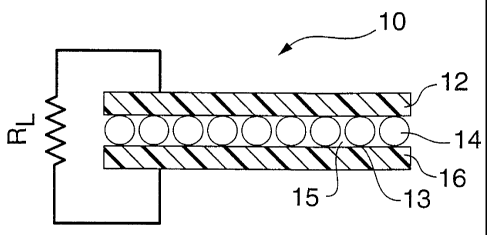
The present invention embodies a thermionic energy converter 10 and is
directed to a method and apparatus for conversion of energy generally
illustrated in
Figure 1. The present invention 10 comprises an electrically and thermally
conductive
electron emitter 12, an electrically and thermally conductive electron
collector 16 for
receiving electrons from the emitter 12, a solid-state barrier 14 disposed
between and
in intimate contact with said emitter 12 and collector 16 for filtering high
energy
electrons transferred from the emitter 12 to the collector 16, and an electric
load
connected to said emitter 12 and collector 16.
The present invention 10 maintains a thermal separation between the emitter
12 and the collector 16 through a fractional surface contact 13, such as that
shown in
Figure 1. Maintaining a thermal separation between the emitter 12 and the
collector
16 provides for ballistic electron transport through barrier 14 and reduces
the transport
of phonons and electrons through thermal conductivity. Hence, the efficiency
is
increased through the collection of ballistic electrons and the reduction of
thermal
conductivity electrons which cannot be collected. It is also important to note
that the
inventive principle works for hole conductivity, as well as for electrons.
Also,
reference to metals herein includes alloys.
The fractional surface contact 13 is defined by a fractional surface geometry
of
decreasing cross-sectional area towards fractional surface contact 13. For
example,
Figure 1 illustrates a fractional surface contact 13 which is defined by a
barrier 14
comprised of spherical particles, wherein the fractional surface geometry is a
spherical
shape. The fractional surface contacts may be integral to the emitter 12, the
barrier
14, or the collector 16. The emitter 12, barrier 14, or collector 16 has one
or more
fractional surface contacts 13 disposed between and in intimate contact with
the
emitter 12 and barrier 14, or the barrier 14 and collector 16, or a
combination thereof.
CA 02367686 2001-09-10
WO 00/59047 PCTIUSOO/05975
8
The fractional surface contact 13 also provides for quantum mechanical
tunneling, for example, along the non-contacting surface of the fractional
contact 13
and between the collector 16 at a distance of 50A or less. This distance
depends upon
the materials utilized and their corresponding work functions. The fractional
surface
contact 13 also provides for thermionic emission facilitated by the reduction
in the
barrier height from image force effects, for example, along non-contacting
surface of
the fractional contact 13 and between the collector 16 at a distance of 25A or
less.
This distance also depends upon the materials utilized and their corresponding
work
functions. See Coutts, T.J. Electrical Conduction in Thin Metal Films. N.Y.,
Elsevier Scientific Publishing Co., 1974, pp. 54-55, for a discussion of the
image
force effect.
Figure 2 illustrates a fractional surface contact 13 having a triangular cross-
section that acts as point emitters or contacts. Other examples of various
fractional
surface contact shapes include, but are not limited to, parabolic-shaped
contacts,
elliptical-shaped contacts, curved-shaped contacts, nanotubes, particles,
dendrites
made from methods such as micro-lithography and holographic lithography,
Tonks'
method (electric instability on liquid metal surface), ion milling, or
equivalents
thereof.
A thermally and electrically nonconductive space 15, including but not limited
to a vacuum, xenon, radon, or other nonconductive gas, is adjacent to the
fractional
surface contacts 13 and the emitter 12 and barrier 14, or the barrier 14 and
collector
16, or a combination thereof. Space 15 reduces electrons that would otherwise
be
thermally transported and assists in maintaining a thermal separation between
the
emitter 12 and the collector 16.
Electron flow occurs when an electrical load RL is connected to the emitter 12
and collector 16, where the work function of the emitter 12 is less than the
work
function of the collector 16. When determining the load resistance, it is
noted that the
maximum efficiency for any electric power source normally occurs when the
internal
resistance of the power source is the same as the load resistance. Therefore,
if the
internal resistance is very low, the desired load resistance should also be
very low.
CA 02367686 2001-09-10
WO 00/59047 PCT/US00/05975
9
If the barrier 14 is adjusted to sort hot electrons, the emitter 12 will be
cooled
and the electron current will result in the potential increase on the
collector 16. To
achieve a desirable converter efficiency, the barrier 14 must effectively stop
electrons
with lower energies. The emitter 12 and the barrier 14 are matched such that
electron
concentration on the emitter 12 is higher than electron concentration on the
collector
16 at a given energy defined by the barrier height.
Utilizing materials with a low reflectance on the emitter side and a high
reflectance on the collector side are beneficial for maintaining a high
efficiency.
1. Emitter
The emitter 12 comprises an electrically and thermally conductive material,
such as metals, metal alloys, semiconductor or doped semiconductor materials.
The
emitter 12 may also comprise an electrically and thermally conductive layer on
a
substrate, such as materials including, but not limited to, Si021 glass,
quartz, or
equivalents thereof, coated with a metallic layer or other thermally and
electrically
conductive material.
Another embodiment of the present invention wherein the fractional surface
contact is associated with the emitter utilizes a high phonon energy material
as the
emitter 12, preferably with a mean energy of at least about 3 kT, to distort
the electron
energy distribution using electron-phonon interaction. Materials exhibiting
these
characteristics are metal hydrides Me,,Hy, irrespective of stoichiometry.
Examples
include, but are not limited to, TiHX, VHX, ZrHX, NbHX, TaHX, ScHX, YHX, ThHX,
UHX
all rare earth hydrides, or combinations thereof Many metals which form
hydrides
may be alloyed with normal metals even to high concentrations without losing
the
high energy component in their phonon spectrum and may have better properties
in
terms of oxidation, e.g., TaCu or TiCu alloys. The emitter 12 should also
provide
thermal and electrical conductivity.
Figure 3 illustrates an example of an emitter comprising a metal hydride
powder 17 supported in a honeycomb structure 18.
In general, all metal hydrides McXH}, have median phonon energy in their
spectra of more than 100 meV, with the exception of Pd and Pd alloys. McXHy is
CA 02367686 2009-06-12
preferable over Me.DY (or McXTY), since the H' isotope is lighter and provides
higher
phonon frequencies (energies). It should also be noted that the phonon
frequency is
basically independent of the hydrogen concentration (See Landolt-Bornstein,
Numerical Data and Functional Relationships in Science and Technology, Group
III:
5 Crystal and Solid State Physics, (1983) Vol. 13b Metals: Phonon States,
Electron
States and Fermi Surfaces, pp. 333-354).
Other stable materials with high phonon energies include, but are not limited
to, BH, B4C, BN (hexagonal), BN (cubic), diamond, or combinations thereof. An
10 emitter 12 using a non-conductive substrate must also have a conductive or
doped
layer, such as silver, with a thickness less than the electron mean free path,
in order to
emit electrons into the barrier 14. Alternatively, the conductive or doped
layer may be
placed on the barrier 14 when the emitter 12 comprises a thermally and
electrically
non-conductive material. A conductive or doped layer provides thermal and
electrical
conductivity. For example, if the emitter 12 comprises BN microspheres and the
conductive or doped layer comprises Ag (electron mean free path is 400A), the
conductive or doped layer thickness is preferably between 50-200A.
2. Barrier
Most semiconductors with a low forbidden gap have a very low thermal
conductivity, such as a few W/(m=K), or roughly 100 times less than for copper
or
silver. This provides for a barrier geometry selection corresponding to at
least a few
degrees of thermal separation between the emitter 12 and the collector 16.
This
embodiment is illustrated in Figures 4A and 4B, wherein a low thermal
conductivity
semiconductor barrier 14 (e.g., fixed pillars, microspheres, etc.) is placed
in a vacuum
between a metal emitter 12 and a metal collector 16. The emitter 12 is at a
higher
temperature than the collector 16. Isotherms (different scale in two
materials) are
indicated by dashed lines 19. The spacing of isotherms 19 is much larger in
metals
due to a larger thermal conductivity. Estimations for a thermal conductivity
difference
of 100:1 result in a bridge cross-sectional linear dimension (e.g., diameter)
of up to
one micron. Area A will then emit electrons, since it is facing a low barrier
on a
CA 02367686 2001-09-10
WO 00/59047 PCT/US00/05975
11
metal-semiconductor interface (a fraction of 1eV). Area B will not emit
electrons,
since it is facing a metal-vacuum interface with a few eV potential barrier.
The ratio
of area A to area B will define the decrease in the thermal conductivity of
the gap
(without a radiation component). For example, a 1:100 ratio provides for a
thermal
separation of 100K between the emitter 12 and collector 16. Decreasing the
emitter
12 area by 100 times will require relatively high current densities. A graph
of the
Richardson current density as a function of the barrier height and temperature
is
shown in Figure 5. Line 20 represents values at 300K; line 22 represents
values at
350K; line 24 represents values at 400K; line 26 represents values at 500K;
line 28
represents values at 700K; line 30 represents values at 800K; and line 32
represents
values at 900K. For instance, a 1 W device having a total area of 1 cm2 and a
temperature of 400K on the emitter 12, will require a Richardson current of
approximately 103A/cm2. This current can be achieved with a barrier of 0.35eV,
such
as PbTe. 104-105A/cm2 is an electromigration practical limit for doped
semiconductors with a small forbidden gap.
The embodiments illustrated in Figures 4A and 4B can be constructed with
known techniques such as micro-lithography or holographic lithography.
However,
thermal expansion characteristics must be considered for certain materials.
For
example, a 1 cm2 metal plate end with a thermal expansion coefficient of 10-5K-
' will
travel 105A at a 100K temperature change, which is inconsistent with a bridge
length
of only a few hundred angstroms. Therefore, the barrier 14 preferably should
be a
moveable (rolling or sliding) barrier. A moveable barrier 14 may comprise
microspheres or short microwires disposed between an emitter 12 and a
collector 16.
Microspheres are preferable because of an absence of thermal expansion and
orientation challenges. The microsphere embodiment is illustrated in Figure 1,
wherein 5-100 nanometer-size semiconductor spheres 14 are available from
precipitation, aerosol, or plasma spray manufacturing methods. However,
advances
in submicron lithography make the nanowire approach feasible from a
technological
point of view. The nanowire approach requires uniform and stress-relieved
materials
on both the emitter 12 and collector 16 sides. The simplest design is a
circular plate
which expands radially. Figure 6 illustrates the expansion pattern 34 and
nanowire
CA 02367686 2001-09-10
WO 00/59047 PCT/US00/05975
12
positioning 36 of a circular plate. It should be noted that plate movement
across the
nanowire may cause degradation after a few thermal cycles, and should be
avoided. A
rectangular plate provides a more complex thermal expansion pattern 38, as
illustrated
in Figure 7. Figure 7 shows that nanowire positioning 40 is relatively complex
and
will be effective when the absolute size change is relatively small to avoid
second
order effects. The plate preferably should have a small thermal expansion
coefficient
to minimize the absolute size change at elevated temperatures.
Circular and rectangular emitter 12 and collector 16 plate geometries are not
the only possible configurations. However, each configuration has its own
thermal
expansion pattern, which must be analyzed mathematically with the nanowire
orientation designed accordingly. A nanowire cross-section can vary depending
upon
the materials used, operating temperatures, and temperature gradients. Some
example
cross-sections 42 include, but are not limited to, those illustrated in Figure
8.
The potential barrier for electrons with this embodiment can be formed only
with Schottky barriers. Examples of known Schottky barriers for some of the
semiconductors in contact with metals are shown in Table 1 below. This list
can be
expanded for basically any Schottky barrier, or when comparing an interface
material's electron work function with the vaccum energy level (See Band
Structure
Engineering in Semiconductor Microstructures, NATO ASI Series, Series B:
Physics,
Vol. 189 (1988), p. 24. Lerach, L. and Albrecht, H. Current Transport in
Forward
Biased Schottky Barriers on Low Doped n-Type InSb, North-Holland Publishing
Co.,
1978. pp. 531-544.; Brillson, L. Contacts to Semiconductors, Fundamentals and
Technology, Noyes Publications, 1993; Rhoderick, E. H. and Williams R. H.
Metal-
Semiconductor Contacts, Second Edition, Clarendon Press, 1988.). Positioning
of the
spheres 14 may be made by precipitation from a liquid, dielectrophoresis,
vibration/charge, masking or equivalents thereof. For example,
dielectrophoresis
involves a powder assuming a charge in a dielectric medium, such as ethyl
alcohol. It
is important to use fresh ethyl alcohol, since the alcohol will pick up water
from the
atmosphere. This will make the medium somewhat conductive and the process will
degrade. The charge moves when an electric field is applied. The controls for
coating
CA 02367686 2001-09-10
WO 00/59047 PCT/US00/05975
13
are the voltage applied and the concentration of powder in the mixture. The
powder is
dispersed by ultra conics or shaking.
As set forth previously, if the emitter 12 comprises a non-metallic material,
a
metallic layer may be placed on either the emitter 12 or the barrier 14. For
example,
the barrier 14 comprising microspheres illustrated in Figure 1 would include
an outer
metallic layer and metal contacts placed on the emitter 12.
CA 02367686 2001-09-10
WO 00/59047 PCT/US00/05975
14
TABLE 1
Material Barrier (eV)
Si 0.5-0.8
n-Ge 0.18-0.45
n-GaAs 0.70
n-InAs 0.50
n-GaSb 0.07
n-InSb -0.1
Sb -0.1
n-PbS -0.2
n-PbSe -0.2
p-Cu20 0.4
p-Se 0.30-0.55
n-CDs 0.88
DySi2 0.37
IrSi3 0.94
Hg,Cd,,_,Te 0.0-0.5
p-Ge 0.26
B (Amorphous) 0.43
LaB6 0.35
YbB6 0.30
Pd2Si 0.7
n-PbTe 0.32
p-GaAs 0.55
n-InP 0.32-0.54
Table 1 shows various materials having a barrier height in the range of 0.1 eV
to 1.0eV. All practical temperatures are included in Figure 5 for the
materials listed in
Table 1. For example, n-GaAs or Pd2Si (0.7eV) are acceptable barrier materials
at an
CA 02367686 2001-09-10
WO 00/59047 PCT/US00/05975
operation temperature of 800K, 1:100 area coverage, and 103A/cm2 current limit
through the barrier material (- 1 W/cm2 converter specific power).
Semiconductors
may also be doped with impurities that provide for sub-band conduction. For
example, doping Ge with Te provides a donar sub-bandwith of 0.3eV spacing from
5 the conductance band bottom, thus changing the intrinsic surface barrier by
a value of
0.15-0.20eV.
An example of the embodiment illustrated in Figure 1 may comprise
O
semiconductor spheres with a I OOA diameter deposited on a variety of
substrates with
a desired density per unit area by methods such as laser ablation, or
equivalents
10 thereof. The surface finish on semiconductors and dielectrics is preferably
within a
few angstroms RMS; however, the surface must be metallized. Metal coatings
with a
1 OA RMS surface are routine with magnetron sputtering. Standard optical
polishing
provides 1-3 arcmin. parallelism. Without a flexible plate on one side, the
absence of
electrical shorts can only be guaranteed over a distance of about 100 microns.
15 Materials having a thickness of approximately 0.1 mm or less such as glass,
quartz, Si,
Ge, mica, or equivalents thereof, will function as a local spring and
compensate for
parallelism if a thermally conductive cushion such as carbon fibers, or
equivalents
thereof, are used as an intermediate layer for compression.
To illustrate thermal management and compression challenges, the
0
embodiment shown in Figure 9 comprises I OOA germanium spheres 44 between two
ideally smooth molybdenum 46 or molybdenum coated plates 48 of lxl cm2
squares,
with a IOOK temperature difference between plates 46 and 48 and a IOW heat
flow
across the converter. One of the plates 46 or 48 is thin enough (e.g., 10-20
microns)
to be sufficiently flexible to compensate locally for parallelism problems.
The heat flow q is supplied by a heat source (not shown). A thermal
differential is maintained between the cold plate 46 at a temperature T, and a
hot plate
48 at a temperature T,. In this case, T, - T, = 100K. Plate 48 is made of a
silicon
O
wafer material having a thickness of 10 microns and metallized with a 2000A
molybdenum coating on both sides. Ge nanospheres 44 are deposited by laser
ablation onto plate 46. A thin layer of carbon fibers 50 provide for a uniform
load on
the plate 48 and conduct heat and electrical flow through the flat compressing
plate
CA 02367686 2009-06-12
16
52. The mechanical load on the nanospheres 44 is regulated by calibrated
springs 54.
In principle, the springs 54 may also be attached to plate 46 instead of plate
52. The
compression force supplied by springs 54 defines the deformation of the
spheres 44,
and indirectly defines the thermal and electric contact properties on the
sphere-plate
interface. The entire device is enclosed in a vacuum chamber and evacuated to
a
residual pressure below 5x10`" torr. At this pressure the thermal conductivity
of air is
smaller than the radiative losses at room temperature (see Kaganer, M.G.
Thermal
Insulation in Cryogenic Engineering. Israel Program for Scientific
Translations Ltd.
1969. Pp7-106.). Kaganer discusses that the thermal resistance on the
interface is a
complex function of many parameters. For simplicity, the following example
assumes
that the thermal resistance of the sphere 44 is equivalent to a rod having a
cross-
section of 1000A2. The specific heat flow (q, = rc5T/oy) through one contact
with a
thermal conductivity, x, value of 40W/(mK) for germanium, yields a value of
4x10'
V. To maintain a I OOK temperature gradient at lOW total heat flow requires
2.5x10⁶
spheres, or approximately 6 micron spacing between the spheres 44, which
corresponds to about 3 arcminutes of plate parallelism that is standard for
thin silicon
wafers.
It can be assumed that under compression the Ge sphere 44 will deform and
the plate 46 will remain flat since the elasticity modulus for Mo (300 GPa) is
much
higher than for Ge (82 GPa). The calculations show that approximately a 1VN
force
is required to provide 1000A contact area. The total compressive force in this
case
will be 0.25N, which is relatively small and allows for only a partial plate
parallelism
compensation with a 10 micron thick silicon plate. Improved results are
possible with
thinner plates or a more flexible plate material such as glass.
The previous example also illustrates the optimization principle for this
device. If the desired temperature differential is increased to 200K, 20 watts
of heat
flow must be supplied to the device. If only 10 watts are available, the
number of
nanospheres must be cut by two, and so forth.
Examples of various barrier 14 materials are disclosed in the following
references: Burstein, E. and
Lundqvist, S. Tunneling Phenomena in Solids. N.Y., Plenum Press, 1969. pp. 47-
78,
CA 02367686 2009-06-12
17
127-134, 149-166, and 193-205. Mizuta, H. and Tanoue, T. The Physics and
Applications ofResonant Tunneling Diodes. N.Y. Cambridge University Press,
1995.
pp. 52-87. Duke, C.B. Tunneling in Solids. N.Y., Academic Press 1969. pp. 49-
158,
and 279-290. Conley, J. W. and Tiemann, J.J. Experimental Aspects of Tunneling
in
Metal-Semiconductor Barriers. Journal ofApplied Physics, Vol. 38, no. 7 (June
1967), pp. 2880-2884. Steinrisser, F. and Davis, L.C. Electron and Phonon
Tunneling Spectroscopy in Metal-Germanium Contacts. Physical Review, Vol. 176,
no. 3 (December 15, 1968), pp. 912-914. Hicks, L.D. and Dresselhaus, M.S.
Effect of
Quantum-well Structures on the Thermoelectric Figure of Merit. Physical Review
B,
Vol. 47, no. 19 (May 15, 1993), pp. 12 272-12 731. Abram, R.A. and Jaros, M.
Band
Structure Engineering in Semiconductor Microstructures. Series B: Physics,
Vol.
189, N.Y. Plenum Press 1988. pp. 1-6, and 21-31. Ferry et al. Quantum
Transport in
Ultrasmall Devices, Series B: Physics, Vol. 342, N.Y. Plenum Press 1995. pp.
191-
200. Shakorui, A. and Bowers, J.E. Heterostructure Integrated Thermionic
Coolers.
Applied Physics Letters, Vol. 71, no. 9 (September 1, 1997), pp. 1234-1236.
One skilled in the art of applying thin barrier materials recognizes the need
for
cleanliness and to avoid contamination such as bacteria, foreign particles,
dust, etc. It
is also important to prepare a smooth surface finish on the substrate on which
the
barrier is placed.
Dielectrics in the pure form have extremely high barrier properties. For
example, a typical forbidden gap for a dielectric is 4-6 eV. It is extremely
difficult to
thermally excite electrons to this kind of energy, in order to provide a
significant
current. Impurities and lattice defects within dielectrics provide local
conductive
bands that give lower barriers.
The behavior of lattice defects and impurities in dielectrics has not been
extensively explored, see e.g., Hill, R.M. Single Carrier Transport in Thin
Dielectric
Films. Amsterdam, Elsevier Publishing Co., 1967. pp. 39-68.
In principle, the barrier height may be controlled
by changing the impurity type and concentration. Conduction by multi-step
tunneling
through defects also provides some conductivity at a low electron energy.
CA 02367686 2009-06-12
18
One skilled in the relevant art recognizes there are a variety of deposition
techniques that may be employed to form ultra thin dielectric coatings, which
include,
but are not limited to, CVD (chemical vapor deposition), PVD (physical vapor
deposition), in their various forms such as magnetron, electron beam, pulsed
laser
deposition, or equivalents thereof. These deposition techniques are known for
the
deposition of 10-500A layers of dielectrics, such as A12O3 and Si02.
The electron energy sorting barrier 14 may also utilize semiconductors, rather
than dielectrics. Since the metal-semiconductor interface barrier can be
selected for a
desired barrier height value, a metal-semiconductor potential barrier can be
more
easily regulated than a metal-dielectric-metal junction. A metal-semiconductor
junction exhibits tunneling properties for highly degenerated semiconductors,
for
example heavily doped semiconductors, which allows for thin potential
barriers.
Three types of semiconductor barriers can be used: (1) conductive or doped
material 62/n-type semiconductor 64/p-type semiconductor 66/conductive or
doped
material 68 (see Figure 10; note also that the n-type and p-type layers may be
reversed); (2) conductive or doped material 70/n-type semiconductor
72/conductive or
doped material 74 (see Figure 11); and (3) conductive or doped material 76/p-
type
semiconductor 78/conductive or doped material 80 (see Figure 12). In this
embodiment, an electron injected into a p-type region can be accelerated by a
local
electric field. Examples of semiconductor materials are disclosed in the
following
references. See Landolt-
Bornstein, Numerical Data and Functional Relationships in Science and
Technology,
Group III' Crystal and Solid State Physics, (1982) Vols. 17b-17i and (1987)
Vol. 22a
Semiconductors. Madelung, 0. Data in Science and Technology. Semiconductors
Other than Group IV Elements and III-V Compounds. N.Y., Springer-Verlag Berlin
Heidelberg, 1992. pp. 1-153. Conwell, E. M., Semiconductors I, Bulletin of
American Physical Society, Vol. 10, (June 14, 1965), p. 593. Hall R. N. and
Racette
J. H. Band Structure Parameters Deduced from Tunneling Experiments, Journal of
Applied Physics, Supp. to Vol. 32, no. 10 (October 1961), pp. 2078-2081.
CA 02367686 2009-06-12
19
With a forbidden gap energy ER, the first barrier will have an exponential
factor E,,, and a second exponential factor of approximately E12 (without a
Schottky
barrier associated with surface defects and crystallography).
Barrier heights for semiconductors are lower than corresponding barriers for
dielectrics. The barrier 14 thickness is not as crucial with a semiconductor
and the barrier
height can be adjusted using a proper semiconductor material. For example, the
semiconductor thickness may be in the region of hundreds of angstroms (or
thicker)
compared to tens of angstroms required for a dielectric. A thicker barrier 14
is much
easier to manufacture because it is less susceptible to pin holes, dust and
other
contaminants. Also, the current exponentially depends on the barrier height.
From Richardson's Equation with a semiconductor having a barrier height tp
equal to 150 meV, the current density at room temperature is very high,
roughly >_ 106
A/cm2 and - 10" A/cm2 at tp equal to about 300 meV. Semiconductors having a
barrier
height of less than 0.6 to 0.7eV may be used in this embodiment, since
reasonably high
current densities (>IA/cm2) may be provided.
A resonant tunneling (RT) barrier 81 comprises two or more barriers 82 and 86
with a spacing 84 between barriers 82 and 86 that is sufficient for electrons
to form a
standing wave (see Figure 13). Spacing 84 is typically 100A or less and
requires a
precision deposition technique, such as molecular beam epitaxy (MBE), or
equivalents
thereof The physics and technology of RT devices is disclosed in Mizuta, H.
and
Tanoue, T. The Physics and Applications of Resonant Tunneling Diodes.
Cambridge
University Press, 1995. pp. 1-235.
The advantage of a resonant tunneling barrier 81 is in its selective electron
energy
dependent transmission. The example of the transmission probability for a
specific
GaAs-Al Ga,_,As heterostructure is given in Figure 14. From Figure 14 it can
be seen
that there are a few transmission peaks, each one of which is a multiple of
the
fundamental harmonics. RT fundamental harmonics can be tuned to a first phonon
harmonics of an emitter material, such as TiH7. Higher harmonics will be
automatically
matched, thereby providing for electrons to be sorted from the Fermi
distribution tail
resulting in higher efficiencies. RT leak currents are extremely small
compared to other
CA 02367686 2001-09-10
WO 00/59047 PCT/US00/05975
types of barriers. For example, the probability of an electron with 0.1 eV
energy to
penetrate the RT barrier 81 is much less than for an electron with 0.25eV
energy. This
type of sorting efficiency provides for a high converter efficiency.
5 3. Collector
The collector 16 material must have the properties set forth below to assure
proper
operation of the converter. The collector 16 must provide thermal and
electrical
conductivity. Figure 15A illustrates a collector 16 having a substrate 88,
which is not
electrically conductive, coated with a conductive or doped layer 90 for
electrical
10 conductivity. If the collector 16 is used as a substrate for the electron
sorting barrier 14,
it must be polished to a surface finish that is superior to the barrier 14
thickness. For
example, with a barrier 14 thickness of 150-200A, the surface finish must be
better than
50A over the entire collector 16. Metals meeting a surface finish requirement
of <50A
are known in the metals optics industry. Such metals include, but are not
limited to, Cu,
15 Mo, W, Al, combinations thereof, or equivalents thereof.
An alternative approach is to utilize optically polished dielectric or
semiconductor
collectors 16, which have good thermal conductivity and are coated with a
conductive or
doped material to achieve the requisite electrical conduction. Such materials
include, but
are not limited to, silicon, gallium arsenide, sapphire, quartz (fused
silica), or equivalents
20 thereof. These materials are readily available with a surface finish better
than 10A. Glass
has a low thermal conductivity of 1-2 W/(m=K) and is therefore only practical
in low
power density converters. Refractory single crystals and diamond can be used
for more
stringent applications.
For embodiments utilizing a high phonon energy material as the emitter 12, the
collector 16 must not have a high energy component in its phonon spectrum.
Moreover,
the collector 16 material must have an atomic mass sufficient to have a
spectrum cutoff
below kT, since the phonon frequency normally decreases with the mass of a
metal atom.
The list of metals meeting this criteria are set forth in Landolt-Bornstein,
Numerical
Data and Functional Relationships in Science and Technology, Group III:
Crystal and
Solid State Physics, (1981) Vol. 13a Metals: Phonons and Electron States.
Fermi
Surfaces, pp. 7-180, and Khotkevich et al., Atlas of Point contact Spectra of
Electron-
CA 02367686 2009-06-12
21
Phonon Interactions in Metals, (1995).
Examples of such metals include, but are not limited to, Au, Bi, Hf,
Pb, Pt, W, Zr, Ta, and Sri.
The thermal expansion coefficient of the collector 16 material preferably
should
be matched to that of the barrier 14 material to prevent coating peel-off
during operation
of the converter under thermal cycling. In addition, the collector 16 material
must have
sufficient mechanical integrity to withstand operation temperatures.
When the materials of the barrier 14 and the collector 16 are not selected so
as to
prevent the leak back of electrons through the barrier 14, an electrically
conductive,
barrier matching material 92 must be disposed between the collector 16 and the
barrier
14 (See Figure 15B). The selection rule for the barrier matching material 92
with an
electron work function tp, an emitter 12 material with an electron work
function (p., and
a barrier 14 material with an electron work function Pb' cis: (pa > Pb a (pe.
The actual 0(p
depends on the operating temperature and application.
The electron energy in an emitter 12, barrier 14, and collector 16 will be
positioned according to their electron work function, when measuring the
electron energy
from the vacuum energy level as a reference point. When the work function of
the
collector 16 material is too low, the collector 16 functions as an additional
barrier for
emitted electrons and, therefore, should be avoided. Metals such as Pt or Ir
have a very
high work function and are preferred. However, they may not be necessary when
the
emitter material has a low electron work function.
4. Examples
4(a). Converter with Dielectric Barrier
A converter was assembled using an emitter comprising tantalum-hydride powder
17 housed in a honeycomb structure 18 (See Figure 3). The converter was
assembled on
a rigid microscope frame with a microscopic linear positioning stage providing
for a
0.5 micron spacing regulation. A cartridge heater (Omega, 100W) was fed with a
regulated DC power supply, and thermal contact to the tantalum-hydride powder
was
provided by a polished copper rod. Both the heater and the rod were enclosed
in Macor
insulation and spring loaded to the microscope stand. A water cooled heat sink
made of
CA 02367686 2001-09-10
WO 00/59047 PCT/USOO/05975
22
copper was mounted on a positioning stage with an additional laser mirror
mount, which
provided for 3D alignment of the contacting planes. Cooling water was supplied
from
a large tank at room temperature by means of a peristaltic pump at 0.5 C
stability over
a one-hour interval. The temperature of the copper rods was measured with two
platinum
RTDs connected to a Keithly 2001 multimeter for data acquisition ( 0.02 C
accuracy).
A stainless steel envelope of each RTD was also used was electric leads to
make a
connecting circuit between the emitter and collector. The voltage in the
external circuit
was measured with a Hewlett Packard model HP34420A nanovoltmeter (R,, = 10
Gigaohm).
A sample I-V curve was measured with a Kepco ABC 25-IDM external power
supply and a Keithly 2001 as an ampmeter. A resistor bank (1 % accuracy) was
connected
in parallel with the circuit, allowing up to 0.5 Gohm loads without
interfering with the
nanovoltmeter. The I-V curve was defined by voltage-load measurements. The
emitter
powders 17 included either TaH or TiH2 particles, ball-milled from an initial
10-20
micron size to 0.2 - 0.3 micron average particle size. The emitter was formed
either by
tapping the powder 17 into a low thermal conductivity honeycomb structure 18
glued to
a copper plate, or by drying a powder suspension in alcohol on the copper
plate. The
honeycomb structure 18 utilized in this prototype was procured from Goodfellow
Corporation, located in Berwyn Pennsylvania. The part number of the honeycomb
structure is AR312610 having the following specifications: 5 mm thickness,
0.05 mm cell
wall, and 3 mm cell size.
A variety of collector substrates were tested, including metallized, optically
polished sapphire, optically polished Kovar and molybdenum, and metallized
optical
glass. A barrier matching material 92 having a thickness of 200-500A was
deposited on
a substrate 90, for example, Ta for a TaH emitter. Dielectric layers of A1203
were
deposited by PVD (physical vapor deposition, magnetron sputtering), or CVD
(chemical
vapor deposition). The impurity, or defect, concentration on the collector
samples,
deposited by both means, was not meticulously controlled. The minimum barrier
thickness achieved, that was not electrically shorted over a 1 cm2 area, was
approximately
250A. In some samples the barrier was not shorted at room temperature, but
failed at 3 5-
C. The highest observed voltage was 0.22V using dielectric barriers at a
temperature
CA 02367686 2001-09-10
WO 00/59047 PCT/US00/05975
23
difference of 35 C between the emitter and collector. The highest observed
current was
about 2 A. Some of the samples had an S-type current-voltage curve, which is
typical
for tunneling diodes (See Figure 16). In Figure 16, the temperature of the
emitter was
approximately 31.96 C, and the temperature differential between the emitter
and the
collector was approximately 11.06 C. The S-curve 94 is not smooth, suggesting
the
existence of a localized conduction band in an amorphous dielectric. Some
samples had
I-V curves 96 and 98 resembling the initial portion of a tunneling S-curve
(See Figure
17). For I-V curve 96, the temperature of the emitter was approximately
22.5'C, and the
temperature differential between the emitter and the collector was
approximately 3.1 C.
For I-V curve 98, the temperature of the emitter was approximately 24.5 C, and
the
temperature differential between the emitter and the collector was
approximately 5.4 C.
In Figure 18, line 100 indicates the voltage dependence on the temperature
gradient,
which was basically linear for most of the samples. The linear V(T) line 100
indicates a
phonon mechanism, which should depend linearly on the heat flow through the
sample.
The heat flow is a linear function of the temperature difference, while the
electron
distribution is an exponential function with temperature.
These tests provided an initial proof-of-concept for a converter with a
voltage
output of up to 10-15 mV/K, which is significantly higher than any known
thermoelectric
device. The current density for the converter utilizing an A1,03 barrier was
low, which
is expected for relatively thick barriers and the absence of conduction band
control.
However, the conduction band can be engineered. Continuous layers of A1203 are
taught
in the literature, with some as low as 20A, and a factor of 106 times gain on
current can
be achieved.
4(b). Converter with Semiconductor Barrier
A converter was made utilizing PbTe coatings as a semiconductor barrier,
deposited by magnetron sputtering. The magnetron sputtering target was 99.99%
pure
p-type PbTe doped with Al to 0.3 - 0.5 atomic %. PbTe has a high electron work
function (4.8 - 5.1 eV) that creates challenges in forming a barrier that will
prevent a
backflow of electrons. Only a limited number of metals have a higher electron
work
function, such as Pt and Au. A polished glass substrate was coated with 3000A
layer of
CA 02367686 2001-09-10
WO 00/59047 PCT/US00/05975
24
Ta for electrical conductivity, with 500A of gold barrier matching, and 350A
of PbTe
as a barrier material. The Schottky barrier height in this case was not known.
At PVD temperatures of 100-200 C, PbTe usually forms a crystalline coating.
The deposition temperature of the sample in this case was 30-100 C; therefore,
an
amorphous coating is not excluded.
Test results are shown below in Table 2, wherein a TaH powder emitter was
utilized with a cross-sectional area of 17mm2. The emitter temperature was
26.9 C and
the collector temperature was 22.0 C. .
TABLE 2
Resistive Load (ohms) Output Voltage (mV)
106 5.2
104 2.7
103 2.4
500 2.3
100 2.2
10 0.020
The results show that the "over the barrier" current was apparently not
achieved,
since the voltage spread is too small, e.g., 5.2mV when compared to an
expected range
of more than 100mV. This means that the actual potential barrier in this case
was more
than, or close to, leV. The conductivity appears to be similar to a phonon-
assisted
impurity conduction band conductivity in a dielectric. Nevertheless, the
recalculated
efficiency of this device was 5.7% of an ideal Carrot cycle without accounting
for the
thermal conductivity of air. The efficiency is 6.6% when taking into account
the thermal
conductivity of air at temperature of 300K and a temperature differential of
4.9K. The
measurement errors were insignificant with 10"3% on the voltage side, I% on
the
resistance (current) side, and 0.02 C on the temperature side. The temperature
drift
during the test was less than 0.2 C.
CA 02367686 2001-09-10
WO 00/59047 PCT/US00/05975
4(c). Converter with Semiconductor Barrier
A converter, similar in construction to the converter constructed in Section
4(b)
above, was constructed from the same PbTe sputtering target (0.3-0.5 atomic %
doping
with Al). The main difference between the present converter and that in
Section 4(b) was
5 the collector substrate, which was polished to 50A RMS surface finish
aluminum (15 x
12 x 3mm3). The Al was coated with 3000A of Ta and 300A of Pt. The PbTe layer
on
top of the Pt layer was 240A. Also, the emitter comprised TiH2 microspheres.
The test was performed with an emitter temperature of 31 0.5 C, and a
temperature difference between the emitter and collector was 7.5 0.5'C. The
resulting
10 I-V curve 102 obtained by varying the load resistor is shown in Figure 19.
The voltage spread was sufficient to resemble over-the-barrier current
transport,
unlike the I-V curve produced in Section 4(b). Efficiency estimations cannot
be made
because the Al substrate has a high thermal conductivity. However, the output
of the
present converter is higher than that produced in Section 4(b).
5. Refrigeration Embodiments
The main components of a thermionic converter 104 for providing refrigeration
(see Figure 20) are essentially the same as those of a thermionic converter 10
for
converting heat to electricity, as set forth above. The essential difference
is that carrier
transport is assisted by an external electric field, Eõxõ and the emitter 12
is connected to
a thermal load. The emitter 12 is thermally insulated by means of an
insulating material
106. Rather than a heated emitter 12, as is the case in the heat to
electricity embodiment,
a thermal load is cooled by heat flow, QLoõd, to the emitter 12 in the
thermionic converter
104 illustrated in Figure 20. The back surface of the collector 16 acts as a
heat
exchanger, and heat flow QLxc/,,,ngc dissipates the heat from hot electrons.
One skilled in
the art of heat exchangers recognizes there are many means for accomplishing
heat
exchange including, but not limited to, air and liquid cooling, or equivalents
thereof.
Barrier configurations that provide for a large thermal separation between the
emitter 12 and collector 16 are set forth above.
It is important to note that phonon-assisted electron transport is less
important in
the refrigeration embodiment than in the heat-to-electricity embodiments,
because the
CA 02367686 2001-09-10
WO 00/59047 PCT/US00/05975
26
refrigeration mode depends primarily on the operating voltage. For example,
there cannot
be more than a 0.3eV gain from phonons at significant currents. The operating
voltage
can be obtained from an external voltage source, E,xt.
Figure 21 illustrates a thermionic converter 108 for providing refrigeration,
which
utilizes a barrier 14 in the form of point contacts. The barrier 14 may
comprise, for
example, spherical semiconductor particles similar to the embodiment
illustrated in
Figure 1.
The barrier 14 illustrated in Figure 22 comprises particles having a thin
semiconductor layer 114 that allows ballistic carrier transport, a conductive
or doped
layer 112 for electrical conductivity and electron work function matching, and
a core
material 110 (see Figure 22). The core material 110 may be a dielectric,
conductive or
doped material, semiconductor, or plastic, if it is sufficiently hard and has
suitable
operating temperatures and thermal expansion coefficients. In this embodiment,
one side
of the particle will function as an emitter and the other side as a collector.
It is also
important to note that the conductive or doped layer 112 must have an electron
work
function value between that of the emitter 12 and collector 16.
6. Applications
Since energy conversion is the basis of modern civilization, an efficient
energy
converter has numerous applications, such as existing utility power plants,
solar power
plants, residential electricity supplies, residential/solar electricity
supply, automotive,
maritime, solar/maritime, portable electronics, environmental heat pump,
refrigeration
(cooling, air conditioning, etc.), aerospace, and so forth.
Power plants have a tremendous amount of waste heat with a potential of 300 C
and lower. Converting the waste heat at 20-40% of Carnot efficiency will give
an
additional 10-20% overall plant efficiency with equivalent savings on fuel.
The proliferation of low-cost converters will lower the capital costs of solar
concentrator power plants with a higher efficiency than current
steam/electricity cycles.
Lower operating temperatures will also lower maintenance costs.
Residential electric supplies based on direct heat to electrical energy
conversion
is ideal for remote areas, where it is difficult or inconvenient to install
power lines. The
CA 02367686 2001-09-10
WO 00/59047 PCT/US00/05975
27
heat source may either be in the form of fossil fuel or solar concentrators.
Solar
concentrators can also be in the form of solar heated water pools, utilizing
day/night
temperature differences. A few hundred cubic meters of water with a hundred
square
meters of surface and cover could provide the electricity supply for a house
in areas with
a temperature differential of about 10 C.
A thermionic converter in combination with a conventional engine driving an
electric generator and an electric motor would substantially increase mileage.
Direct energy conversion has tremendous application in electric cars. One
application involves using thermionic devices with operating temperatures up
to about
150 to 200 C as overall efficiency boosters. Another application is an
automobile with
an electric drive and a conventional engine coupled with an electric generator
having a
converter array as an intermediate radiator.
Automotive and propulsion applications are also applicable to maritime
applications. In addition, solar concentrators may be used in a sail-type
fashion. A
combination of light and inexpensive plastic Fresnel lenses with thermionic
converters
may be incorporated into modern rigid wing-type sails, providing for the use
of wind and
sun energy to propel a boat with about 100-200 W/m2 of the sail solar
component.
Since the converter can utilize very small temperature gradients in a self-
sustaining mode, a temperature gradient between the heat sinks will be created
with
asymmetric heat exchange on the surface (e.g. one heat sink can be thermally
insulated).
Also, the system will run until something malfunctions, cooling the
environment and
producing electricity. In summary, the method and apparatus disclosed herein
is a
significant improvement from the present state of the art of thermionic energy
conversion.
The invention may be embodied in other specific forms without departing from
its spirit or essential characteristics. The described embodiments are to be
considered in
all respects only as illustrative and not restrictive. The scope of the
invention is,
therefore, indicated by the appended claims rather than by the foregoing
description. All
changes which come within the meaning and range of equivalency of the claims
are to
be embraced within their scope.
What is claimed and desired to be secured by Letters Patent is: