Note: Descriptions are shown in the official language in which they were submitted.
CA 02367828 2001-09-17
WO 00/58782 PCT/GBOO/01216
AN OPTICAL CROSSPOINT SWITCH USING VERTICALLY COUPLED
WAVEGUIDE STRUCTURE
An optical crosspoint switch structure is
disclosed. The switch permits light signals to be
diverted from any of arbitrary number of input ports to
any or several of an arbitrary number of output ports.
The switch consists of two groups of intercepting
optical waveguides formed on a planar substrate, which
are the input and output waveguides respectively. At
each intersection, another waveguide is formed above
the input and output waveguides. Optical coupling
between this upper waveguide and the input/output
waveguides is controlled by an electrical or optical
signal. The upper waveguide has a corner mirror at the
intersection. When the control signal allows, light
couples from the input waveguide to the upper
waveguide. After being reflected by the corner mirror,
the light couples from the upper waveguide into the
output waveguide. The upper waveguide incorporates the
active switching element, allowing high modulation
depth and low crosstalk level.
FIELD OF INVENTION
The present invention relates to optical
components and in particular to an optical crosspoint
switch array structure.
DESCRIPTION OF THE RELATED ART
An optical crosspoint switch array is used in an
optical communications system/network to route light
signals. It allows light to be diverted from (1) any
one of input ports to any one or more output ports
(routing), (2) several input ports to an equal or lower
SUBSTITUTE SHEET (RULE 26)
CA 02367828 2001-09-17
WO 00/58782 PCT/GBOO/01216
-2-
number of output ports in an arbitrary order (shuffling
or combination), and, (3) any one input port to several
output ports (broadcasting). The switch can have an
arbitrary number of input and output ports and is
designed to be readily scaleable. The realisation of
these functions important applications in an optical
communications network.
Three main kinds of conventional structures for
optical crosspoint switches have been proposed. The
first kind splits all optical inputs into a number of
branches, as described by Kato, T., et al, in IEICE
Trans. On Electronics, Vol.E82C, No.2 pp.305-312, 1999.
The number of branches equals the number of outputs.
Then it seeks to regroup and recombine these branches.
Switching is performed by blocking these branches
before recombination. The second kind uses two groups
of perpendicular waveguides on a planar substrate as
inputs and outputs, respectively. Switching is
achieved by constructing couplers in the same plane, as
described by Fish, G.A., et al, IEEE Photonics
Technology Letters, Vol.10, No.2, pp.230-232, 1998.
The third kind also uses two groups of perpendicular
waveguides on a planar substrate as inputs and outputs,
respectively. Switching is achieved by constructing
directional couplers in the vertical direction using
only refractive index change as the switching
mechanism, as described in "analysis of an InGaAsP/InP
twin-overlayed-waveguide switch" by R. Maciejko, A.
Champagne, B. Reid, and H Mani, In IEEE Journal of
Quantum Electronics, 1994, Vol.30, No.9, pp.2106-2113.
However, the first kind of structure has the
disadvantages that it has a high insertion loss
proportional to the number of outputs and that it uses
large substrate area. The second kind of structure has
SUBSTITUTE SHEET (RULE 26)
CA 02367828 2007-06-01
-3-
the disadvantages that it uses large substrate area. The
third structure has the disadvantage that high modulation
depths and low crosstalk levels are difficult to achieve.
SUMMARY OF THE INVENTION
Illustrative embodiments of the invention may provide an
optical crosspoint switch scheme employing vertical optical
coupling with high modulation depth and minimum crosstalk
levels between channels.
Illustrative embodiments of the invention may also
provide an optical crosspoint switch occupying a small area
per crosspoint (input/output pair).
One particular illustrative embodiment utilises
simultaneous refractive index and optical gain changes in the
upper waveguide.
Another particular illustrative embodiment utilises
simultaneous refractive index and optical absorption changes
in the waveguide coupler.
In accordance with one such illustrative embodiment of
the invention, as embodied and broadly described herein and
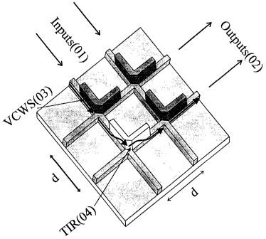
illustrated in Fig. 1, two groups of intersecting waveguides,
namely the input (01) and the output (02) waveguides, are
formed on a planar substrate of an appropriate material. Near
each crosspoint, another layer of waveguide is formed above
the input and output waveguides, forming a vertically coupled
waveguide structure [VCWS (03)]. Vertical optical coupling
between this upper waveguide and the lower input/output
waveguides is controlled by an electric or optical signal. The
upper waveguide has total internal reflection [TIR (04)]
corner mirror at the crosspoint. When the control signal
CA 02367828 2007-06-01
-4-
selects one particular switch, light couples from the input
waveguide to the upper waveguide fully or partially. Reflected
by the corner mirror, the light is steered by an angle, then
couples from the upper waveguide into the output waveguide.
High modulation depth and low crosstalk level are achieved by
changing the optical absorption and/or gain in the waveguides
synchronously with the switching action.
In illustrative embodiments, the thickness and the
refractive index of the lower layer, the upper waveguide layer
and the spacing layer between them may be designed so that the
coupling length is reduced to the extent that the distance
between adjacent ports is decided by the space needed for the
input/output optical fibre coupling.
In one particular embodiment of the invention, the lower
waveguide, the spacing layer and the upper waveguide layer are
consequently formed on a semiconductor substrate suitable for
the signal wavelength, to produce a wafer. The bandgap of the
lower waveguide is such that it is transparent at the signal
wavelength. The bandgap of the upper waveguide is such that it
provides high optical absorption when there is no carrier
injection, and provides optical gain when there is carrier
injection. The propagation constants of the two waveguides are
so designed that, when there is no carrier injection, the
lower waveguide has smaller propagation constant than the
upper waveguide. The doping profile of the layers ensures that
most injected carriers are confined in the upper waveguide.
To achieve another particular embodiment of the
invention, the lower waveguide, the spacing layer and the
upper waveguide layer are consequently formed on a III-V
semiconductor substrate suitable for the signal wavelength, to
CA 02367828 2007-06-01
-5-
produce a wafer. The bandgap of the lower waveguide is such
that it is of low optical loss at the signal wavelength. The
bandgap of the upper waveguide is such that it provides high
optical absorption when there is applied electric field, and
is of low optical loss when there is no applied electric
field. The propagation constants of the two waveguides are so
designed that, when there is no applied electric field, the
two waveguides have equal propagation constants. The doping
profile of the layers ensures that electric field will be
applied mostly across the upper waveguide.
In accordance with an illustrative embodiment of the
present invention, there is provided a method of controlling
an optical crosspoint switch. The switch includes
intersecting input and output waveguides forming an
intersection, an upper waveguide having a first portion which
is arranged adjacent to the input waveguide and which extends
at least partially along the input waveguide from the
intersection, a second portion which is arranged adjacent to
the ouptut waveguide and which extends at least partially
along the output waveguide from the intersection, and a corner
mirror located adjacent to the intersection for coupling light
signals from the first portion into the second portion. The
upper waveguide is made of a material having characteristics
such that application of an electrical signal thereto causes
variation of the loss/gain characteristics and refractive
index profile thereof. The method includes applying an
electrical signal to the switch such that in an OFF state of
the switch, the refractive index profile of the upper
waveguide is varied substantially to prevent light being
vertically coupled between the first and second portions of
the upper waveguide and the input and output waveguides
respectively. In an ON state of the switch, the refractive
CA 02367828 2007-06-01
-5A-
index profile of the upper waveguide is varied to enable
light to be vertically coupled between the first and second
portions of the upper waveguide and the input and output
waveguides respectively. In the ON state of the switch, the
loss/gain characteristics of the first and second portions of
the upper waveguide are varied to enhance vertical coupling of
light between the first and second portions of the upper
waveguide and the input and output waveguides respectively.
In accordance with another illustrative embodiment of the
invention, there is provided an optical crosspoint switch.
The switch includes intersecting input and output waveguides
forming an intersection. The switch further includes an upper
waveguide having a first portion arranged adjacent to the
input waveguide and extending at least partially along the
input waveguide from the intersection, a second portion
arranged adjacent to the output waveguide and extending at
least partially along the output waveguide from the
intersection, and a corner mirror located adjacent to the
intersection for coupling light signals from the first portion
into the second portion. The switch is characterised in that
the upper waveguide is made of a material having
characteristics such that application of an electrical signal
thereto causes variation of the loss/gain characteristics and
refractive index profile thereof, such that in an ON state of
the switch, light is vertically coupled between the input
waveguide and the first waveguide portion and between the
second waveguide portion and the output waveguide, and in an
OFF state of the switch, light is substantially prevented from
being vertically coupled between the input waveguide and the
first waveguide portion and between the second waveguide
portion and the output waveguide.
CA 02367828 2007-06-01
-5B-
Aspects and advantages of the invention will be set forth
in part in the description which follows, and in part will be
obvious from the description, or may be learnt by practice of
the invention. Aspects and advantages of the invention may be
realised and attained by means of the elements and
combinations particularly pointed out in the appended claims.
BRIEF DESCRIPTION OF THE DRAWINGS
The accompanying drawings illustrate embodiments of the
invention and, together with the description, serve to explain
the principles of the invention.
CA 02367828 2001-09-17
WO 00/58782 PCT/GBOO/01216
-6-
Fig. 1 illustrates the configuration of the
optical crosspoint switch array with 2 inputs and 2
outputs, which can be extended to arbitrary numbers of
inputs and outputs.
Figs. 2A and 2B illustrate schematically
propagation of the light signal at each cross point
with control signal at "on" and "off" states,
respectively. A plan (top) view and a perspective view
are included in each state.
Figs. 3A and 3B illustrate schematically
propagation of the light signal in the first particular
embodiment of the invention, with distributions of
optical refractive index (n) and absorption in both
"ON" and "OFF" states.
Figs. 4A and 4B illustrate schematically
propagation of the light signal in the second
particular embodiment of the invention, with
distributions of optical refractive index (n) and
absorption in both "ON" and "OFF" states.
Fig. 5 shows the layer structure of a wafer on
which the array is fabricated.
Fig. 6 shows the layout of a 4x4 switch array.
Fig. 7 illustrates a switch unit cell.
Fig. 8 shows the switching characteristics of the
switch unit cell.
DESCRIPTION OF THE PREFERRED EMBODIMENTS
Reference will now be made in detail to the
SUBSTITUTE SHEET (RULE 26)
CA 02367828 2001-09-17
WO 00/58782 PCT/GBOO/01216
-7-
preferred embodiments of the present invention, two
examples of which are illustrated in accompanying
drawings.
One preferred embodiment of the present invention
will be explained hereinafter with references to the
accompanying drawings.
At the "ON" state, carriers are injected into, and
confined in the upper waveguide of Fig. 3. The upper
waveguide may comprise bulk or quantum-well III-V
semiconductor material such as InGaAsP, which, at the
signal light wavelength, provides optical gain with
adequate non-equilibrium carrier concentration but is
highly absorptive when there is no such carrier
concentration. The refractive index of the upper
waveguide at the signal wavelength will be reduced due
to the existence of these carriers, causing the
reduction of the propagation constant of the upper
waveguide to a value close to that of the lower
waveguide. As a result, strong optical coupling
happens between the two waveguides, enabling the
transfer of signal from the lower input waveguide to
the upper waveguide, and after reflected by the corner
mirror, its transfer from the upper waveguide to the
lower output waveguide. At the "OFF" state, there is
no injected carrier, the unequal propagation constant
of the two waveguide layers reduce optical coupling to
a weak extent. In the absence of injected carriers,
high optical absorption in the upper waveguide ensures
that the weak signal light that does couple into the
upper waveguide is absorbed and does not couple into
the output waveguide. High modulation depth and low
crosstalk level is therefore achieved. This embodiment
of the invention has the additional advantage of
providing optical gain to compensate for the losses
SUBSTITUTE SHEET (RULE 26)
CA 02367828 2001-09-17
WO 00/58782 PCT/GBOO/01216
-8-
which may occur in the crosspoint switch or other parts
of the optical transmission link.
Another preferred embodiment of the present
invention will be explained hereinafter with references
to the accompanying drawings.
At the "ON" state, no electric field is applied
across the upper waveguide of Fig. 4. As a result,
strong optical coupling happens between the two
waveguides because of their equal optical propagation
constants, enabling the transfer of signal from the
lower input waveguide to the upper waveguide, and after
reflected by the corner mirror, its transfer from the
upper waveguide to the lower output waveguide. At the
"OFF" state, an electric field is applied across the
upper waveguide, increasing both its refractive index
(therefore its optical propagation constant) and its
absorption. The unequal propagation constant of the
two waveguide layers reduce optical coupling to a weak
extent. The high optical absorption in the upper
waveguide ensures that the weak signal light that does
couple into the upper waveguide is absorbed and does
not couple into the output waveguide. High modulation
depth and low crosstalk level is therefore achieved.
Other embodiments of the invention will be
apparent to the skilled in the art from consideration
of the specification and practice of the invention
disclosed herein. It is intended that the
specification and examples be considered as exemplary
only, with the true scope and spirit of the invention
defined by the claims.
An optical crosspoint switch array combining such
features as compactness, high speed, and low crosstalk
SUBSTITUTE SHEET (RULE 26)
CA 02367828 2001-09-17
WO 00/58782 PCT/GBOO/01216
-9-
level is highly desirable in high speed all-optical
networks. Demonstrated devices based on various
guided-wave components so far appear unable to achieve
these qualities simultaneously. One kind of crosspoint
switches employs MMI couplers to split all optical
inputs into a number of branches. Then it seeks to
regroup and recombine these branches. Switching is
performed by blocking these branches before
recombination. This kind of crosspoint switch has a
high insertion loss proportional to the number of
outputs and uses large substrate area. A second kind
of switch uses two groups of perpendicular waveguides
on a planar substrate as inputs and outputs,
respectively. Switching is achieved by constructing
directional couplers in the same plane, as described
in. This also uses large substrate area. The present
switch structure uses the coupling of light in the
vertical direction (normal to the substrate plane, see
Fig. 7. to switch any input signal orthogonally to any
output (Fig. 8.) Ultra-low crosstalk level at the "OFF"
state is achieved by rendering the coupler to a
weakened coupling and a high absorption state
simultaneously, so that any stray signal is
sufficiently attenuated. By careful design, the
couplers are made short, allowing the switch to be
compact, but tolerant to fabrication variations. The
component switch mechanism should allow switching on
nanosecond timescales.
DEVICE DESIGN AND FABRICATION
The crosspoint switch array presented here is
fabricated on a InGaAsP/InP wafer whose layer structure
is illustrated in Fig. S. It contains two waveguide
layers which are grown by MOVPE on (100) InP substrate.
The undoped upper waveguide core which contains 5
SUBSTITUTE SHEET (RULE 26)
CA 02367828 2001-09-17
WO 00/58782 PCT/GBOO/01216
-10-
unstrained 65A InGaAs quantum wells with Q1.26 barriers
serves as the active layer at the wavelength of 1550nm.
To control the optical coupling between the two
waveguide layers, the effective refractive index of
passive lower waveguide core is adjusted to a suitable
value lower than that of the active waveguide by
incorporating an appropriate number of quantum wells of
37A thick. The passive waveguide has a low absorption
for wavelengths of 1500nm and above. Both waveguide
core layers are 0.3mm thick, separated by a 1.2mm thick
InP spacing layer. The spacing layer and the passive
waveguide core are n-doped to 3x10¹⁷/cm3, as well as the
lower InP cladding. The design of this is such that
effective switching can be achieved over the entire
gain bandwidth of 50nm of the active layer. Two
perpendicular groups of ridge waveguides are formed on
the wafer as input and output waveguides, respectively.
The waveguides in each group are 3mm wide and 250mm
apart. At present 4x4 switch arrays are fabricated
(Fig. 2) but it is easy to scale up to any input/output
numbers. The upper active waveguide layer is removed
from the waveguides except for a 200mm length extending
from the intersections toward both the input and output
ports, as illustrated in Fig. 3. Vertical optical
directional couplers are formed between these active
waveguide layer and the lower passive waveguide layer.
A total internal reflection mirror (TIR), the depth of
which penetrates the upper waveguide, is formed
diagonally cross the waveguide intersection. Switching
mechanism is provided by carrier induced refractive
index changes in the active upper waveguide of the
coupler, which change the coupling length of the
vertical coupler [3]. At the "ON" state, the effective
refractive index of the active upper waveguide is
reduced to equal that of the lower waveguide by the
presence of injected carriers, therefore the input
SUBSTITUTE SHEET (RULE 26)
CA 02367828 2001-09-17
WO 00/58782 PCT/GBOO/01216
-11-
optical signal will couple strongly from the passive
input waveguide into the upper active waveguide,
reflected by the TIR, then couple from the upper
waveguide to the output waveguide. The injected
carriers also provide optical gain for the signal,
therefore contributing the high ON/OFF contrats. Low
crosstalk level at the "OFF" state (no carrier
injection) is achieved by the combination of much
weakened signal coupling into the active upper
waveguide and the highly absorptive nature of the
active upper waveguide to any residual coupled signal.
At the OFF state the input light travels to the next
unit cell through the lower passive waveguide. The
structure is defined by a reactive ion etching process
using H2/CH4 plasma. A combination of metal and
dielectric mask materials are used to facilitate the
two-level dry-etching, and to produce smooth and
vertical sidewall finish required by the TIR. The
depth of the TIR mirror is about halfway between the
two waveguide layers. The structure is finished with
Polyimide planitization and Ti/Au contacts. The arrays
(Fig.3) are then cleaved from the wafer, allowing 100mm
passive access waveguides at both input and output
ports. Individual switches are also cleaved from the
arrays for characterisation.
RESULTS:
Preliminary characterisation results is presented
here for a single switch unit cell. The switch cell
has 100mm input and output passive waveguides, with the
input waveyuide extending beyond the intersection for
500mm. An HP8168E tuneable laser source is used to
produce input signal in the wavelength range of 1470-
1580nm. The signal is coupled in and out of the device
via fibre lenses. A fibre polarisation controller is
SUBSTITUTE SHEET (RULE 26)
CA 02367828 2001-09-17
WO 00/58782 PCT/GBOO/01216
-12-
used to produce either TE or TM polarised input signal.
An optical filter is used to eliminate most of the
spontaneous emission from the output signal.
The optimum switching characteristics, plotted in
Fig. 8, is achieved at 1=1548nm (the gain peak
wavelength of the active waveguide) with TE input
polarisation. It is shown that in the "OFF" state,
i.e., when injected current is zero, the measured
crosstalk signal level is as low as -79dBm for an in-
fibre input signal power of -5dBm. Accounting the
total loss of about 14dB including input/output
coupling and the optical filter, the on-chip crosstalk
is about -60dB, which to our knowledge is the lowest
reported so far. The ON/OFF contrast at 70mA is as
high as 45dB while an maximum of >50dB is achieved for
injection current of 160mA.
CONCLUSION
An compact integrated 4x4 optical crosspoint
switch array has been fabricated on InGaAsP/InP
substrate which employs active vertical couplers to
achieve compactness, low crosstalk level and high
ON/OFF contrasts. Preliminary results show that the
switches can achieve on-chip crosstalk levels as low as
-60dB and a high ON/OFF contrast of greater than 50dB.
The switching time for the device is being tested and
is believed to be in the nanosecond range determined by
the carrier lifetime. Further results will be
presented at the conference.
4x4 optical crosspoint switch arrays based on the
first preferred embodiment and the second preferred
embodiment have been designed, fabricated and tested.
The devices are fabricated on InP substrate. The area
SUBSTITUTE SHEET (RULE 26)
CA 02367828 2001-09-17
WO 00/58782 PCT/GBOO/01216
-13-
of a 4x4 array is only 1.2x1.2mm, with an distance of
0.25mm between adjacent input or output waveguides.
The crosstalk level at input wavelength of 1548nm is -
60dB. The modulation depth (ON/OFF contrast) is 50dB.
The fabrication and testing results are described in
detail in the appending paper authored by the
inventors.
SUBSTITUTE SHEET (RULE 26)