Note: Descriptions are shown in the official language in which they were submitted.
CA 02367878 2001-09-18
WO 00/58840 PCT/IB99/00529
1
AMPIC DRAM SYSTEM
The present invention relates to the validation of dsta to be read at a I~RAM
bank
prior to such being read, to insure that it is current and up-to-date data;
beinb more
particularly, though not exclusively, directed to.such validation of data
react out of a
mufti-port internally cached DRAM memory system of the type described in co-
pending
US patent applicailon serial No.58l,467, filed December 29, 1995, for I-libh
Performance Universal Mufti Port Intewally Cached Dynamic Random Access Memory
System, Architecture and Method, by Mukesh Chatter, and ofcommon assignee
herewith, and to the ability to optimize the performance ofsuch a device with
a minimal
amount of complexity.
SACK ROUND
In mufti-ported internally cached dynamically accessed memory systems (AMP1C
devices) - - a new paradigm in shared memory core switching described in said
co-
pending application and hereinat~er more fully explained, - - independent
serial interface
cache data is written into the AMPIC device before writing it into shared
internal DRAM
banks, ovary which contention arises. The caching oFthe data received on the
serial
interfaces reduces the chances that internal contention to a particular DRAM
bank will
affect the overall external performance of the serial interfaces by increasing
the nurnber
of requests that may be outstanding to a particular internal AMhIC DI~AM bank
before it
CA 02367878 2001-09-18
WO 00/58840 PCT/IB99/00529
2
becomes necessary to stop the writinb of information on one of the external
serial
interfaces in order to avoid overrunning the limited write cache space far the
particular
serial interface. Because of the potential for a large number of read and
write access
requests to he contending for a particular DRAM bank, the time it takes the
AMPIC
device to write data into one rrf the infernal DRAM banks can significantly
vary up to
some finite maximum amount of time. If data is written to a particular address
in one of
the internal DRAM banks within the AMPIC and that sartte address is requested
before
the written data moves from the write cache into the actual C~RtIM bank
location
specified by the address, the old data (or stale data) currently stored at
that address wilt
be returned instead c~f the newly written data in the event that the read
access to the
DRAM bank should be granted before the write access.
Thus, it is desirable to have a method vf~;zraranteeing that a read operation
to a
specific internal DRAM bank address returns the data that was last written to
that
particular address prior to the read operation; or to provide some means
ofreturning
information to the logic that generated the read request, stating that the
data at the
requested AMPIL device address is not up to date, The present invention
addresses this
need by novel data validation methods that thus enhartce the performance and
cache
coherency ofthe AMPIC switching architecture.
In other types of digital systertts, data validation mechanisms are used for
microprocessor caching and for networking data transmission validation, but
these
tnechanisms differ I;reatly in purpose and in implcmentatidn from the
invention described
in. the present application for use with the AMPIC technology.
CA 02367878 2001-09-18
WO 00/58840 PCT/IB99/00529
Designers of microprocessors have used memory caching techniques for some
time, for example, to ease the bottleneck in processor performance between a
processor
and its memory. Basically, the processor keeps duplicate copies of smaller
sections of
what is in the main memory in a Faster caching memory to improve performance.
There
is, however, the problem of keeping the duplicate copies of data up-to-date,
or having the
carne value. Most cachins algorithms focus an ensuring that when data is
changed in the
cache, the corresponding data in main memory is immediately updated (caching
write-
through schemes), or is marked as needing to be updated in the future ("dirty
bit" caching
schemes). This memory validation problem is much different from the data
switching
problem of the present invention in that one source, the microprocessor,
controls the
contents of the cache that it uses for main memory. For the AMPIC technology,
of the
invention, on the other hand, there are many sources and many caches that are
controlled
independently of one another and all used in conjunction to keep the data in
the DRAM
banks of the AMPIC devices up to date. Solving the problem of having many
sources
and caches for the AtviPlC technology is therefore very different from the
microprocessor
:aching techniques that have heretofore been developed for microprocessors.
Another area 'sn which validation schemes have been previously used is in data
link protocols fur the transmission of data froth a source to a destination in
networking.
These protocols are used to guarantee that the data received is actually the
data scnt.
Most oft~hese protocols allow only a limited number of packets to be
transmitted until the
receiver acknowledges correct reception of the packets, By including a
sequence
number, these protocols allow the receive side to identify the last correct
packet that it
received, indicatinb on which packet the transmitter should start sending
al;ain. By
CA 02367878 2001-09-18
WO 00/58840 PCT/IB99/00529
4
limiting the number of packets that the transmitter can have outstanding at
one time to be
less than the number of packets that can be identified by the sequence number,
it can be
guaranteed that bath the transmitter and receiver can communicate which
packets were
lost and which need to be retransmitted. The most common of these data link
layers is
the "sliding window" protocol described, for example, in C:QMpUTEK NETWORKS,
2"'~
Edition, by Andrew S. Tanenbaum; pages 212-228, using such seduence numbers.
While
these data link protocols are designed to determine when packets were
transmitted
incorrectly from one to another across noisy data communication lines, they
are not
applicable to the validating of data retrieved From an AM>'IC 1~RAM memory and
the
race condition that makes the validation scheme of the present invention,
necessary: In
the sliding window protocol mr~reover, the receiver passively waits to receive
the next
packets and determines what to do next when the packet comes in with its
sequence
number.
Quite differently, in the present invention. data is placed in AMPIC devices,
informing the destination of the existence of this data, and enabling the
destination then
actively to fetch the da;a. In this invention, furthermore, specialized logic
is provided in
the AMPIC devices themselves to ensure that only valid data or appropriately
marked
invalid data is transmitted back to the destination source.
OBJErLTS OF INVENT1 N
The primary object of the present invention, accordingly, is to provide a
novel
method of and apparatus for guaranteeing that only valid data is read out of a
mufti-port
CA 02367878 2001-09-18
WO 00/58840 PCT/IB99/00529
internally cached DRAM device (AMP(C), thereby eliminating any race condition
in
which stale data could potentially get read out of an AMP1C device before the
desired
data has actually been written into the appropriate internal AN1PIG DRAM
banks.
A further abject is to provide such an apparatus that can avoid dead-lock
situations that may arise when the AMPIC device can nc~t identify and return
valid data
within some finite amount of lime.
An additional object is to enable the scaling of the apparatus such that it is
equally
efficient with an array of AMPIC devices to validate data.
Other and further objects wit! be explained hereinafter and are more
particularly
delineated in the appended claims.
UMMARY
In summary, from one of its broader aspects, the invention provides methods of
guaranteeing that only valid data is read from a single mufti-port internally
cached
DRAM device (AMtaIt=') or an array ofsuch devices, where a plurality of system
1/0
resources read and write data into and nut ofan AMP1C device or devices
through
independent serial interfaces that contain caching to optimize the utilisation
ofthe shared
internal IaRAM banks,
Iv9ore particularly, the invention embraces in a mufti-port internally cached
array
ofAMpIC DRAM devices in which a plurality ofsystem IIO resources write and
read
data into and oat of DRAM banks through independent serial interfaces and
along shared
internal data busses connected to corresponding DRAM banks in each unit of the
array, a
CA 02367878 2001-09-18
WO 00/58840 PCT/IB99/00529
G
method, that comprises, checking the data stored at a particular address in a
f)ftAM bank
before reading out therefrom tv a requesting system ilc~ resource, to
guarantee against
that data being stale, as frorfi~ bus contention delays that have potentially
prevented
updated valid data from havin g been written into the bank before it is
requested to read
out; and upon such checking that the data is up-to-date, uansferring such
valid data to the
requesting system li0 resource.
Preferred and best mode designs and techniques are hereinafter presented in
detail.
DRA'W1NGS
The invention will now be described in connection with the accompanying
drawings in which;
Fig. 1 is an illustrative block diagram of the internal architecture of the
AMPIC DRAM
of said co-pending application, the operation ofwhich is enhanced by the
present
invention;
Ficg. 2 is a block diagram of an illustrative system architecture based on the
AM151C
DRAM of Fig_ 1:
Fig. 3 illustrates a system in which a totally self contained AMpIC data
validation
scheme will not work;
Fig. 4 shows one type df system with a separate control and data path that
requires some
system level data validation scherne;
Fig. 5 illustrates how the stale bits are stored within all of the multi-port
internally cached
DRAM memory when the apparatus shown in I~ig. 6 is used;
CA 02367878 2001-09-18
WO 00/58840 PCT/IB99/00529
7
Fib. G illustrates the preferred apparatus for and method of providing a novel
mechanism
and technique for guarantecin~: only valid data is read out oCa multi-port
internally
cached TaRAM memory device (AMPIC device), in accard.ance with the present
invention;
rig. 7 illustrates a modification that, though not completely operating to
l;uarantee only
valid data read-out as in the system of Fig. 6, is still useful at least to
identify the
existence of stale or bad data; and
Fib. 8 illustrates where the stale bit is stored within the data in the AMPIC
memory banks
when using such modification that jcrst identiCves bad data read from AMPIC
memories.
PREFERRED EMBODIMFNT(~) OF THE INVENTION
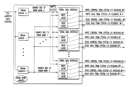
A5 previously noted, the basic structure provided by the AMPIC DRAM device of
said co-pending application is illustrated in Fib. 1, providing a very high
bandwidth
connection between system IlO resources #O through #Y-I, applied at data ports
or pins
n to corresponding serial interfaces O through Y-1 to DRAM memory array banks
O
through ~-1 located within the AMPIC DRAM device. The architecture illustrated
in
Fib, i is all - encompassing of the different AMPIC memory devices that can be
created
by varying the number X of DRAM banks, vaiying the number Y afserial
interfaces, and
varying the number 'n' of data pins per serial interface. In addition, the
arrows showing
the flow of data and control information into and out of each serial data
interface O.,.Y-1
are intended to represent all combinations of serial interfaces which can
provide the
required data and Control t7ows shown,
CA 02367878 2001-09-18
WO 00/58840 PCT/IB99/00529
8
A system I/O resource far the purpose of the present invention refers to a
block of
logic that requires the ability to read and write data into an ANIPIC device
or a group of
AMPIC devices. The AMPIC device shown in Fig. 1 provides a rnechanisen for
transferring large amounts c~fdata from one system IIU resource to another,
granted that a
source system I/O resource can inform a destination system 1/0 resource that
is has
placed data at a specific address inside of the AMPIC device for that
destination system
I/O resource. ?he AMPIC device contains 'x' internal DRAM banks each of which
has
'k' number of merrrory locations in it, resulting in a total of 'x*k' memory
locations to
which variable sized data blocks can be read and written. The maximum
allowable data
size is fixed by the particular implementation of the AMPIC device. Each of
the AMP1C
memory addresses identifies a particular memory location in a particular
internal DRAM
bank, to which data can be written and read thrauah all of the serial data
interfaces shown
in FiI;. 1. All system I/O resources can read and write all ofthe AMPIC memory
locations through the serial interface to which they are connected.
From the I/(~ resources, shown to the right of the ANIPIC Device in Fig. l,
write
control and write data busses connect with the right-hand inputs of the serial
data
interface and to the write cache ofthe interface; for example, from system
I/(.7 resource
#4 to serial data interface O. The read control bus is similarly applied to
the interface O
and to its read cache, which also connects tn the read data bus of system Il0
resource O.
All the serial interfaces share a common bus to act:ess Dram bank O. 'this
shared bus is
independent c~f the shared bus that all of the intei faces use to access DRAM
hank l,
allowing different serial interfaces to be accessing the different DRAM banks
at the same
CA 02367878 2001-09-18
WO 00/58840 PCT/IB99/00529
9
time. Overall, there are X-1 independent shared busses that the Y~ 1 serial
interfaces use
to access the X-1 BRAM banks,
'fhe CPU port may have its own busses into each c>f the I7ILAM banks, as shown
in Fig. l, or it may also share the same busses that the serial interfaces
must share to
access the DRAM banks,
'I'hus, each system I/O resource has a write control bus and a write data bus
connected to one of the AMPIC device serial interfaces to write data into the
AMPIC
device. To write a variable sized block of data into the AMPIC device, a
system I/O
resource sends an AMPIC address on its write control bus and the variable
sized block of
data on its write data bus. As the serial data interface on the AMPIC receives
the address
and data, it places such into the before-mentioned write cache of that serial
data interface.
After completing the current write operation into the serial data interface to
which a
particular system I/O resource is connected, it can immediately start writing
another
variable sized data burst to another AMPIC device address. As more data is
written into
the AM.PIC on one serial data interface, the write cache may fill up faster
than it can be
emptied. To keep the write cache on each seriai interface from overflowing,
each serial
interface has the means to stall (or temporarily stop) the current data write
transfer until
enough space has been freed up in the write cache to finish completing the
current write
transfer. The serial data intei face signals the system il0 resource to stop
sending data
through the system I/O resource write control bus. As data is written into the
write cache
of each serial data interface, the serial data interfaces request access to
'x' internal
DRAM banks in the AMPIC device.
CA 02367878 2001-09-18
WO 00/58840 PCT/IB99/00529
1 (~
The schematically represented DRAM hank arbiters (there being one arbiter for
each DRAM bankl grant tire ditterent serial data interfaces access to the DRAM
banks of
the AMPIC device, allowing, the serial data interfaces to move the data tom
the write
cache into the proper memory location in the internal DRAM banks. The write
caching is
used in the serial data interfaces to help smooth aver periods of contention
when multiple
serial data interfaces are attempting to vvrite data into the same DRAM bank.
When too
many requests are outstanding to the same DRAM bank from the different serial
interfaces, however, some of the seriat interfaces are forced to stall the
current write
operations, as before-mentioned, in order to prevent their write caches from
being
overflowed,
In addition to the write control and data busses, as previously stated, each
system
1l0 resource has a read control bus and a read data bus connected to one ofthe
AMPIC
device serial interfaces to read data from the AMPIC device. When a system
I/C)
resource wants to read the variable sized data block (orated at a particular
AMPIC
address, it writes the address into the AMP1C serial data interface to which
it connects on
its read control bus. The serial data interface on the AMPIC places the
address in the
read cache until it can gain control of the internal DRAM bank in which the
data is stored
and read it out. After retrieving the data, the serial data interface
transmits the variable
sized data block back to the system I/Q resource. Because of the uncertainty
of the delay
in reading data from an AMP1C address, the AMPIC device is designed such that
data
from several addresses can be requested and stored irr the read cache before
the first
variable sized data block is fetched and returned, This allows multiple blocks
of data to
be requested and retriPV~~d out of the DRAM banks at the same time. The AMP1C,
CA 02367878 2001-09-18
WO 00/58840 PCT/IB99/00529
however, preserves the order that the addresses were inserted and wil! only
transmit the
data retrieved back to the system 1/0 resource in that nrder.
The flexibility of the AMPIC device is further enhanced by its ability to
'stack'
multiple AMPIC devices into an array of AMP1C devices to create a much largci
virtual
AMPIC device, as illustrated in Fia. 2, showinb AMPICa 0,1... M-1, each of the
type
shown in Fig. 1. This makes it possible to scale the data busses from the
array of AMPIC
devices or virtual AMPIC device to m*n bits that attach to 'y' system Il0
resources,
where there arc 'm' AMPIC devices used, each of which has 'n' bits of data oil
the serial
interfaces to read and write inforrtiation into the ~AMPIC devices. This
increases the data
rate at which data can be written into and read out of a single AMPIC device
by 'm'
times, and also increases the maximum amount of data that can be stored at
each memory
location to m times its size in a single AMPIC device. When rnultiple AMPIC
devices
are collected into an array of AMPIC devices and used as one large virtual
AMPIC
device, as shown in Fig. 2. all 'm' devices are clock cycle - synchronized,
meaning that
even though no control wires connect the AMPIC devices together, the 'm'
AM1'IC
devices will stay perfectly synchronized because the exact same read and write
accesses
are performed on all 'm' AMPIC devices at the same time. It should also be
observed
shat because the exact same read and write accesses are performed on all 'm'
AMPIC
devices at the same time, there are the same number of AMPIC addresses ft~r a
single
AMP1C 8evice as there are for a virtual AMPIC device. A member of AMPIC
devices
synchronized together is herein sometimes referred to either as an array
ofAMPIC
devices or as a virtual AMPIC device; and discussion about a single AMPXC
device also
CA 02367878 2001-09-18
WO 00/58840 PCT/IB99/00529
12
directly applies to a virtual AMPIC device and vice versa, because a virtual
AlvlPiC
device is simply multiple AMPIC devices working in parallel.
Since the serial interfaces share the same internal DRAM busses to the DRAA4
banks, as shown in Hig 1, to put data into the DRAM banks and take it out, it
is
inevitable that contention will occur for these shared resources some
statistical percent of
the time, thus causing the time it takes to read or write data into and out of
the internal
DRAM banks inside the AMf~IC memory to have a significant variance with some
guaranteed upper bound. In an effort to alleviate the majority of this
contention, extra
buffering or caching is provided such that a few write accesses can be stored,
as
described above, before reaching the point of having to stall one of tha
external serial
interfaces to one of the systenn Il0 resources. By buffering a few write
operations in the
serial interface, the majority of times, that contention occurs, such is
alleviated before
having to stall any of the external serial data interfaces. Similarly, some
level of caching
is provided for the read accesses such that multiple read requests can be
stored and
handled simultaneously tv the DRAM. banks, reducing the chance that no data
will be
present to send to a particular system Il0 resource.
This non-deterministic timing afthe AMPIC device or virtual AhIPIC device can
potentially create a race condition where it becomes possible for the
destination system
IIQ resource actually to request data before it has had time to be read out of
a write cache
data written into its destination internal AMPIC device DRAM bank. Although it
is
probably possible to implement some logic to stop the transmission of data
that has been
identified as being held up in one ofthe serial interface write caches, the
logic: required to
check all the write caches far a particular address becomes a monstrous task
when
CA 02367878 2001-09-18
WO 00/58840 PCT/IB99/00529
considering doing this far all requested addresses and for all seria! ports,
and in fast,
orderly fashion. In addition, if there are any pipelined ingress write
transfer blocks of
I~gic, so-labeicd in Fig. 3, and that nribht be required for a number of
reasons, any data
validation scheme entirely contained within a single AMPIC device or virtual
AMPIC
device will be inadequate because the AMPIC device will not 6e cognizant of
the
existence ofthe write operations in the ingress write transfer logic. An
example of a
system in which such ingress write transfer logic might be required is a
system in which a
set of backplane transceiver chips are required to send the write addresses
and data across
some type vfhigh-speed serial interface beforc~fransferring the write
information into the
AMPIC device itself. Any data validation scheme that is going to be successful
for such
a system, therefore, must start at the same place at which the address is
chosen for where
to place the data in the AMPIC.
Figure 4, illustrates one such type of system that has a separate control and
data
path in which an array of AMPIC devices or a virtual AMPIC device is used, and
for
which a systern data validation scheme will be required to ensure that valid
data is~read
out of the AMPIC devices. It is possible, indeed, for addresses tn circulate
around the
separate control path and get inserted into the AMPIC,' DRAM devices before
the data far
the addresses have been written into the internal 17RAM AMPIC banks. One
natural
cause of this in such a system will be unusual statistical events in which a
large number
of addresses from different system l/0 resources are all outstanding and
contending to be
read or written to the same single internal DRAM bank in the AMpIC device or
virtual
AMPIC device, which could potentially prevent data from being written into the
bank
before it is read out.
CA 02367878 2001-09-18
WO 00/58840 PCT/IB99/00529
14
The novel apparatus and method ofthe invention can readily be implemented for
guaranteeing that only valid data'is read out Af the multi-port internally
cached DRAM
memory (AMPIC device), and also providinb for avoiding dead-lock situations
that may
arise when the AMPIC device or virtual AMPIC device can not identify and
return valid
data within some finite amount of time. Systems like the one 5howo in Fib. 4
can
therefore be readily modified to provide that the system 110 resources are
buaranteed to
obtain correct data, or appropriately marked invalid data, when the system IIO
resources
read the data out of a single AMPtC device or a virtual AMPIC device in the
system.
The invention works at the system level such that any amount of pipelined
ingress
write logic and any amount of pipclined egress read logic can be used without
affecting
the data validation scheme of the invention. The data validation scheme of the
invention
associates an extra tit, termed a ''stale bit" herein, with each address
location within an
AMP1C device or virtual A1~4PIC device, and incorporates a new stale bit
checking
scheme into the architecture of the AMPIC device. lay having the system IIO
resources
use the stale bit in the data validation method described below, the array of
AMPIC
devices within the system is able to ensure that only valid data, or properly
marked in-
valid data, is read from the AMPIC devices by the system 1/0 resources.
This data validation technique requires that the one extra bit be stored with
the
data at each address location within each AMPIC device contained within the
array of
AMPIC devices. Fig. 5 shows the details of how the extra yr stale bit checking
scheme is
incorporated in each AMPIG device to ensure that valid data is retrieved
correctly from a
virtual AMr'IC device. For simplicity and clarity, Fig. 5 only shows exemplary
system
1/0 resource 0 write control, system IJU resource 0 write data, system UO
resource Y-1
CA 02367878 2001-09-18
WO 00/58840 PCT/IB99/00529
read control, and system I/0 resource Y-1 read data busses, instead of~showing
all the
system I/O resource busses as in Figs. 1 and 3.
The data validation technique of the invention requirES that the system I/p
resource know the state of the stale bit for an address which.corresponds to a
location in
one of the internal DRAM banks before the system I/O resource writes data to
that
AMP1C address, While the details of how the system 110 resource maintains this
information is later discussed, for present purposes of explanation, it is
first assumed that
all of the stale bit locations at all of the addresses in the AhZPIC devices
in the array are
set to zero.
During a write operation, the system I/O resource must insert an address and a
stale bit through its write control bus into the same serial interface on each
of the AMPIC
devices in the array of A.MPIC devices, while the different bits of the data
are distributed
and written into different AMPIC devices in the array through the same system
1/0
resource write data bus. As the same address, the same stale bit and different
data are
received on the same serial interface on different AMPIC devices in the array,
the
address, stale bit and data are written into each AMPIC device serial
interface write
cache. The data is then moved into the appropriate internal DRAM bank after
that serial
interface has been granted control over that particular DRAM bank. It should
be noted
that this happens on the same serial interface on all the AMPIC devices
contained in the
virtual AMPIC device at the same time because al! AMPIC devices in a virtual
AMP1C
device are always synchronized, as previously explained.
At some point after the write operation, a different system Il0 resource or
possibly the same, one may attempt to read the newly written data out of the
virtual
CA 02367878 2001-09-18
WO 00/58840 PCT/IB99/00529
iG
AMPIC device. The system I/O resource that wants to read the data, inserts the
address
and stale bit through its read control bus into all the AM9PIC devices in the
virtual
AMPIC device. Each serial interface on the different AMPIC devices in the
array, all
performing; the same action at the same time, write the address and state bit
into their read
cache. When the serial interfaces of the virtual AMf IC: device obtains access
to the same
infernal DRAM bank in the virtual AMPIC device, the data is read out of the
DRAM
bank t~>gether with the written-in stale bit_ If the stale bit inserted over
the read control
bus matches the stale-bit read out from the DRAM, al) of the serial interfaces
connected
to the system IlQ resource that read the address from the. virtual AMPIC
device transmit
their section of the data back to that system 1/0 resource.
If the stale bits do not match the data read from the address, however, the
address
is read from the DRAM banks until the stale hits match, or until a fixed
amount of time
expires. If the fixed amount of time expires and the stale bits still do not
match, the serial
interface on the virtual A>tIPIC device connected to the requesting I/0
resource will sel
an error bit in the data being transferred back so that the system IIO
resource that
requested the data will know that the data is not valid.
The specific example in Fig. 5 shows the address Ox5 and a stale bit of one
being
written through the system 1/0 resource O write control but into the serial
interface 0 on
all of the AMP1C devices in the virtual AMP1C device, while different bits of
data AAA,
BBB andCCC: are written to the different A1~1PIC devices through the system
I/0 Q
write data bus. Serial interface O on all the AMP1C devices in the virtual
AMPIC device
then temporarily stores this data into its write. cache until the serial inter
face obtains
permission to write the data into the appropriate location in the appropriate
DRAM bank.
CA 02367878 2001-09-18
WO 00/58840 PCT/IB99/00529
17
In Fig. 5, furthermore, the system 1l0 resource Y-I reads address 0x5 by
inserting that address and a stale bit of one into the serial interface Y-1 on
all of the
AMP1C devices in the, array 0, I ,..M-1. The serial interface Y-1 on all of
the AMPIC
devices in the virtual AMPIC device then fetches its section of data from the
internal
DRAM bank specified by the address. In parallel, the serial interface Y-1 on
each
AMP1C device in the virtual AMP1C device uses the stale checking logic to
compare the
stale bit inserted for the read access with the one that was read out of the
internal DRAM
bank location. if the stale bits match, the data is sent out an the Y-1 serial
interface on all
the AMPIC devices in the virtual AMPIC device to system I/O resource Y-1 that
read~it.
lCthe stale bits do not match, the data has not been placed in the AMPIC DRAM
bank
yet, and all of the of Y-1 serial interfaces on the AMP1C devices will fetch
the data from
that address location again and compare the stale bits again. This process
continues until
a data value is fetched that has a stale bit that matches the state bit that
was inserted on
the read control serial interface, and the data frorn the address is sent to
the system 1/0
resource that requested it. To avoid a dead-lock situation where the two stale
bits may
never match one other; each AMPIC read access is only allowed to be
outstanding for a
finite maximum predetermined amount of time. if that amount oCtime expires
before the
stale bits match, an error bit is set in the data that is passed back to the
system I/O
resource. This prevents the AMP1C devices from entering a dead-lock state when
an
error in the system occurs, and yet still provides the system 1/0 resource
information so
that it will not use invalid information.
Fig. 6 includes flow chart information "A"-"F" showing what niust.be done in
the
system far this data validation scheme to work properly. hirst, the stale bit
located in the
CA 02367878 2001-09-18
WO 00/58840 PCT/IB99/00529
18
data at every address must be programmed to zero in alt of the AMPIC devices
in the
array through the CPU control interface ("A"). This ensures that all of the
system IIO
resources know the state of all the stale bits for the addresses that they
will use. Because
the stale bit is inserted on the CPU control interface, it goes to all AMPIC
devices in the
system, not just one Ah9pIC device. After all the memory addresses have been
initialized to have a stab bit of zero, a number of addresses are handed out
to each of the
system 1/O resources along with the information that when the address is first
used, a
stale bit of I should be used with the addresses ("B"). When an address is
used for the
first time, the stale bit is set tv one and is passed into all the AMPIC
devices in the virtual
AMPIC device with the address on the write control path ("C"). After
completing the
transfer, the source 110 resource sends a message to the destination I/O
resource with the
address and stale bit ("D"). The destination tl0 resource takes and inserts
both the
address and stale bit into all of the AMP1C devices over its read control path
("E"). As
described previously, the AMPIC devices will continue to fetch the data out of
the
particular memory location in one of the internal DRAM banks either until the
stale bit
inserted on the read control bus matches the stale bit stored with the data or
until some
finite amount of time has passed with no success. if the stale bits match, the
data is sent
back to the system I/O resource that requested the data. If; however, the
stale bits never
match, an error bit is set within the data that is returned to system 1/0
resource that
requested it, allowing the system I/0 resource to discard that data instead of
using invalid
data.
After the destination system Il0 resource receives either the valid data, or
the
marked invalid data, it sends a message across the control path to the source
system I/0
CA 02367878 2001-09-18
WO 00/58840 PCT/IB99/00529
19
resource saying that it is done with the address ("1-"). The source system 1IO
resource
then flips the stale bit associated with the returned address so that the next
time it uses the
address, it will know to use the opposite value for the stale bit ("G"). By
flipping the
value of the stale bit for a particular address each time a source I/O
resource uses it, the
AMPIC device internal stale checking logic can validate that data being sent
to the
system I/4 resources is valid or invalid.
A modification that, while not achieving all the verification and control
features
of the prefetrcd system of Fig_ 6, is useful at least to identify the
existence of stale or old
data, is presented in Fig. 7, it employs a stale bit with each address in the
AMP1C
memory device, and works ut the system level to provide an easy means for
determining
if the data retrieved from a requested address is valid or not. To achieve
this result, one
bit must be set aside in the same place of the data at every address in the
virtual AMPIt'
device. When the AMPIC memory first powers-up, the stale bit stored in the
data at
every address must be written to a zero through the AIvtPIC CPU interfaces
("A"). After
writing the stale bit at every address to a zero, ownership of a number of
addresses is
given to each system ll0 resource, along with the information that when the
system I/U
resource first uses each of the addresses, it should set the stale bit in the
buffer to one
("B"). When a buffer is used for.the first time, the stale bit put in the data
is set to 1
("C"), which is opposite to the setting of the stale bit of the data inside
the AMPIC for
that address. After transferring the data that contains the stale bit to the
AMPIC devices
in the virtual AMPIC device, the source system I/O resource then must send the
destination III resource a message through the control path, stating that
there is data
available for it in a particular address with a stale bit of 1 ("D"j. The
destination system
CA 02367878 2001-09-18
WO 00/58840 PCT/IB99/00529
I10 resource can then retrieve the data by inserting the address into the
AMPIC device or
array ofAMPIC devices (''E"). lVhen the data from the address is returned to
the
destination system I/O rtsource from the virtual AMPIC device, the destination
system
l/0 resource can compare the stale hit contained in the data with the one that
was sent to
it by the source system IlU resource. If the two stale bits match, the data is
the correct
data that was sent. If the stale bits do not match, it means that the ingress
data had not
been written into the appropriate internal AMPIC DRAM bank in the virtua!
AMPIC
device by the time the address contents were requested by the destination l/a
resource. If
the destination I/Ct resource wants to try to get the correct data again, it
can simply re-
insert the address a second time in hopes that in the period of time sirzoe it
received the
incorrect data, the correct data was written into the internal DRAI~4 bank in
the AMP1C
devices.
This process of comparinb the stale bits after data is returned for the
address can
be iterated until the correct data is finally retrieved. After the destination
I/O resource
has either rrarieved the correct data from the AMPIC devices or decided to
give up re-
requesting the data after a number of tries, the destination I'O resource
sends the source
IIU resource a message through the control path telling it that it can use the
address again
("F"). The next time around, when the address is used again, the stale bit in
the data
written to the address will be set to O since the stale value in the AMFIC
memory devices
will now be vne f"G") . Ry constantly flipping the stale bit each time ofuse
of a
particular AMP1C: address, the stale bit always provides enough information to
determine
whether the data is the most current data, or the last data left over from the
previous data
transfer.
CA 02367878 2001-09-18
WO 00/58840 PCT/IB99/00529
21
Fig, 8 makes clear that in this data validation method of Fig. 7, the stale
bit
actually resides in the data written to the AMPIC address and therefore only
gets stored
into one ofthe AMPtC devices in the virtual AMPIC device. This modified method
of
performins data validation can be used with a virtual AMPtC device that
provides no
internal stale checking scheme to create a system where all data read from
AMPIG
devices is validated before being used, providing a reliable method of
ensuring that all
data read out of the AMPIC devices is corre~;t. There are, however, some
downsides to
performing; the data validation in this manner. First and mast impr~rtantly,
in order to
keep the system I/O resource egress pipes full, it is necessary to request
data from
multiple addresses before the data from the first address starts to cone back.
If the stale
bit of the first data returned is incorrect, more data read from different
addresses comes
back from the array of AMP1C devices immediately ai~er the bad data. Since the
data
was requested in a particular order and the source I/O resource wants that
data in that
order, the easiest thing; to do is throw away all of the data that comes back
after the stale
mis-compare, and re-request all c~f it from the virtual AMhIC device again.
Obviously.
this drastically reduces the bandwidth utilisation of each system I/O resource
whenever
there is a state bit mis-comparE, not only because time is wasted sending back
a
potentially large chunk of useless data, but since a few more addresses worth
of data also
had to be thrown out and re~requested. A second disadvantage in using this
data
validation method of Fip,s. 7 and 8, as compared with the system of Fig, G, is
that the
implementing logic required to do the state bit compare and re-insertion of
addresses that
have invalid data returned is fairly complex when implementing it on the Il0
resource,
CA 02367878 2001-09-18
WO 00/58840 PCT/IB99/00529
22
while the internal stale bit checking scheme of h'ig, G, implemented in the
AMP1C
devices themselves, is actually quite simple.
Further modifications will occur to those skilled in this art and such are
considered to fall within the spirit and scope of the invention as defined in
the appended
claims.