Note: Descriptions are shown in the official language in which they were submitted.
CA 02368057 2001-09-14
WO 00/56130 PCT/SE00/00493
A METHOD AND AN ARRANGEMENT FOR THE EI~ECTRICAI~ CONTACT OF
COMPONENTS
FIELD OF INVENTION
The present invention relates to a method for connecting a
component, such as a chip or like component, to a conductive
carrier surface, such as an earth plane on a printed circuit
board or the like, in a compact design, and also to an
arrangement for connecting a component so as to achieve
conduction between said component and a carrier, such as
between a chip and a printed circuit board,. in a compact
design.
DESCRIPTION OF THE BACKGROUND ART
It is known to mount substrate 1 with chip 2 on printed
circuit board 3. In compact designs, with a multi-layer
ceramic carrier substrates, the discrete components/the chips
are mounted on the underside of the substrate between said
substrate and the printed circuit board, wherewith heat
generated in the components can be transmitted solely to the
substrate and from there to the circuit board and its various
connections, such as contact pins or beads 4 of solder that
melt at high temperatures located between the substrate and
the printed circuit board. The connections function as
electrical connections and as mechanical spacing means, this
latter by virtue of being slightly larger than the remaining
discrete components on the underside of the substrate. The
components can be shielded by providing on the circuit board,
immediately beneath the components, an earth plane 5 which,
together with the earth plane of respective components,
shields said components without the discrete components being
in contact with the earth plane. The substrate-mounted
components are liable to generate heat in operation, which in
certain cases may be quite considerable. It is therefore
CA 02368057 2001-09-14
WO 00/56130 PCT/SE00/00493
2
important that the thermal contact achieved between the
components/the chips and the printed circuit board with its
wide copper surfaces is as effective as possible. Because
none of the discrete components have direct contact with the
circuit board, the major part of the heat generated in said
components must be transferred to the circuit board via the
substrate and the circuit board connections . In the case of
ceramic substrates, the greatest temperature gradient occurs
in the longitudinal direction of the substrate in these
instances, because ceramics are relatively poor conductors of
heat. Transistors in the components may well become damaged
at excessively high temperatures, as a result of the poor
thermal conductivity of the ceramic substrate.
SUMMP~RY OF THE INVENTION
With the intention of protecting a component, such as a chip,
that is mounted on a ceramic substrate connected to a
carrier, such as a printed circuit board, from damage as a
result of the limited thermal conductivity of the ceramic,
the chip has been connected directly to the circuit board
with a thin layer that provides the absolute shortest path to
the circuit board. Direct connection of the chip with the
circuit board can be achieved by soldering the chip so that
its height, which is critical, will be essentially the same
as the height of the connections, and by mounting the rear
side of the chip directly to the circuit board with a thin
layer of adhesive or solder. An acceptable substrate earth
can be obtained, by metallizing the rear side of the chip and
making the connection between the rear side of the chip and
the earth plane on the printed circuit board electrically
conductive.
The invention will now be described in more detail with
reference to preferred embodiments thereof and also with
reference to the accompanying drawing.
CA 02368057 2001-09-14
WO 00/56130 PCT/SE00/00493
3
BRIEF DESCRIPTION OF THE DRAWING
Figure 1 shows a chip connected to a carrier-mounted
substrate in accordance with known technology.
Figure 2 shows a chip connected to a substrate which is
mounted on and connected to a carrier in accordance with the
invention.
Figure 3 shows a chip connected to a substrate mounted on and
connected to a carrier-mounted cooling element. in accordance
with the invention.
DESCRIPTION OF PREFERRED EMBODIMENTS
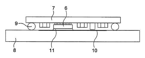
In response to requirements for a compact design, such as a
design which in respect of components is particularly created
for embodiment in telephones or other similar applications,
there has been created a new type of module in which
discrete components/chips 6 have been mounted on the
underside of a carrier substrate 7 that is comprised of
several ceramic layers, between said substrate and a printed
circuit board 8, so as to be in contact with said board. In
this case, the. connections between substrate and printed
circuit board are also comprised of beads 9 of solder that
melts at high temperatures. The beads function as electrical
connections and also as mechanical spacing means, by virtue
of being slightly larger than all other discrete components
on the underside of the substrate. The printed circuit board
may include immediately beneath the substrate-mounted chip an
earth plane 10 which, together with the earth plane of the
chip, electrically shields sensitive parts of the chip. With
the intention of improving the thermal and electrical
properties of the chip, the chip has been connected directly
to the circuit board with the aid of a thin conductive layer
CA 02368057 2001-09-14
WO 00/56130 PCT/SE00/00493
4
11, because of the limited thermal conductivity of the
substrate ceramic. This provides the absolutely shortest
thermal path to the circuit board. Direct connection of the
chip can be achieved by adapting chip height, which may be
critical, so that the height of the soldered chip will be
almost the same as the height of the beads, or balls, and
then fastening the rear side of the chip directly to the
circuit board with a thin conductive layer of adhesive or
solder. When the rear side of the chip is metallized and the
connection between the rear side of the chip and the earth
plane on the circuit board are made electrically conductive,
there can be obtained, at the same time, effective substrate
earthing of the chip. When the rear side of the chip/chips 6
is metallized and a conductive connection 11 to the circuit
board 8 is provided, specific chip cooling elements 12
provided on or in the circuit board can be connected directly
to the chip/chips.
Contact between chip and circuit board can conceivably be
effected in chiefly two ways, either by gluing or soldering.
In conjunction with soldering the module, the chip can be
glued firmly in position by introducing some additional
process steps, subsequent to having applied solder paste to
the circuit board, by pressing for instance and after having
dispensed adhesive to the circuit board where the chip is to
be placed. The adhesive or glue used may conveniently be of a
kind which will cure in conjunction with the re-melting
process. No electrically conductive contact on the rear side
of the chip is required in order to obtain solely thermal
contact between chip and circuit board. However, a rear-side
contact is required in contact with an electrically
conductive adhesive, when effective substrate-earthing of the
chip is required.
The chip can be soldered to the circuit board without
requiring any additional process steps. It is necessary,
CA 02368057 2001-09-14
WO 00/56130 PCT/SE00/00493
however, that the chip has a solderable rear-side contact,
and that the chip is fixed to the ceramic substrate with a
bottom filling, so that there is no danger of the chip being
moved out of its position when beads or balls of low-melting
5 solder, so-called flipchip bumps, are re-melted. The
soldering process per se is very simple, since an earth plane
is already present beneath the chip/chips. All that may be
required is to make an opening in the protective varnish
present beneath the chip, and that a solder paste is also
applied in this region.
It will be understood that the invention is not restricted to
the aforedescribed and illustrated exemplifying embodiments
thereof, and that modifications can be made within the scope
of the accompanying Claims.