Note: Descriptions are shown in the official language in which they were submitted.
CA 02368161 2002-O1-16
Low Loss and Low Polarization Dependence Waveguide Variable Optical
Attenuator
Technical Field
The present invention is a variable optical attenuator using a Mach-Zehnder
interferometers configuration and polarization dependence compensator. It
relates to a
variable optical attenuator with low insertion loss and low polarization
dependence for
optical communication systems and simultaneous testing systems of multiple
parameters.
Background of the Invention
Development of fiber-optic telecommunication systems has exactly passed a
whole
process of the dramatic growing and the rapid falling. This whole process not
only has
stimulated new microstructure optoelectronic technologies instead of
mechanical
individual devices, but also given us how to focus on feasible new products
with reliable
technologies. Among various microstructure optoelectronic technologies,
integrated
optics represents a promising strategy in these advanced oprical information
areas. One
implementation of this strategy relies on the waveguide technology. The thermo-
optic
(TO) waveguide devices using PECVD-based silica-on-silicon have shown an
exciting
advantage over the currently used mechanical and bulk optic devices in fiber-
optic
telecommunications because of their great flexibility in fabrication and
processing as well
as speedy operations than the mechanical ones. The electro-optic (E0)
waveguide
devices using diffused LiNb03-based waveguides have also presented a promising
application in the future with its high-speed operation, Iow loss and mature
manufacturing technology. But, the fabrication of LiNb03-based electro-optic
waveguide
devices is really has its own limitation. Polymer, as a new kind of EO film
material,
always receives much research aimed at solving its stability and
manufacturability.
Recently, research on practical EO polymers has really had some significant
progresses.
Thus, developing new high-performance EO waveguide devices also gives a new
hope to
industry. Among all the active devices in both optical communication systems
and
simultaneous testing of multiple parameters, the optical space switches are
certainly key
components. But, in these two typical cases, variable optical attenuators are
indispensable
to protect the detecting equipments from damaging. Especially, in these two
cases,
variable optical attenuator arrays are strongly requested for the signal
protection of
optical multiple channel systems. Thus, the arrayed variable optical
attenuators based on
plannar waveguides technology will play an increasingly critical role in
emerging
multichannel and reconfigurable photonic networks such as the dense wavelength
division multiplexing (DWDM) and the simultaneous testing systems of multiple
parameters together with optical switches.
Most of both variable optical attenuators and optical switches in production
today use
an opto-mechanical means to implement optical attenuating and steering. This
is
accomplished through the separation, or the alignment by an opto-mechanically
driven
optical parts. These designs offer good optical performance, but have two main
drawbacks. One is slow speed. The typical settling times for operating from 10
ms to 100
ms. And the other drawbacks includes the noise and size. In an era when the
use of
CA 02368161 2002-O1-16
electronics is considered an intrusion in the all-optical networks,
mechanically based
devices seem out of place. Especially, this design is really hard to meet the
marketing
needs for the arrayed variable optical attenuators. To overcome some of these
limitations,
non-mechanical and no-moving-part variable optical attenuators and optical
switches
based on the integrated optical technology are paid much research and
development in
the past a few years. But, the main critical obstacles blocking these efforts
from
challenging the conventional products based on the opto-mechanical designs are
system
loss and polarization dependence. But, both the EO and the TO waveguides for
these two
main active components have shown a huge potential of applications not only in
the
operation speed, but also in compatibility with integrated optic circuits.
Totally there are two typical designs of Mach-Zehnder interferometer (MZI)
configuration for waveguide variable optical attenuators. One uses two 3dB
couplers and
its operation is based on the controlling of optical coupling process between
two
waveguide channels. This design is the same as the 2x2 optical switches by
using a pair
of cross-state input/output ports. The other one uses two Y junctions and its
operation is
based on the splitting and interfering of optical beams with waveguides. These
two
designs of waveguide variable optical attenuators have some similar properties
and some
different optical characteristics at both the unattenuated state and the
attenuated state. For
example, they have similar attenuating process with the applied power for the
thermal
modulating (or the electric voltage for the electrical modulating) and the
same power
consumption for the same attenuated level with the same waveguides structure.
But, they
have different system losses at the unattenuated state and different
polarization dependent
losses at the same attenuated level. The design based on 3dB couplers
generally has
lower system loss at the unattenuated state and higher polarization dependent
loss at the
attenuated state than the design based on Y junctions.
Summary of the Invention
A waveguide variable optical attenuator using a pair of waveguide 3dB couplers
configuration and having a polarization dependent loss compensator is proposed
in this
invention. This pair of 3dB couplers forms a Mach-Zehnder interferometer where
a pair
of cross-state input port and output port is used. One modulating electrode is
made on one
arm of the Mach-Zehnder interferometer and used to change the optical phase of
the
modulated arm. The modulating form can be either thermal-optic or electro-
optic. This
structure has some advantages over the other typical one that uses a pair of Y
junctions.
Generally the access loss of a 3dB coupler is much less than that of a Y
junction, so the
system loss of the waveguide variable optical attenuator based on this
invention is much
less than that of the other typical structure of the variable optical
attenuators based on a
pair of Y junctions. Generally, the polarization dependent loss is a vital
issue for a
variable optical attenuator with either the 3dB couplers structure or the Y
junctions
structure during it is being attenuated. Even at the attenuated states, the
polarization
dependent loss of the waveguide variable optical attenuator with the 3dB
couplers is
higher than that of the waveguide variable optical attenuator with the Y
junctions. In this
invention, a polarization dependence compensator is introduced to correct any
polarization dependent loss to the acceptable level. The operation principle
of this
polarization dependence compensator is to rotate the polarization of the
optical beam by
CA 02368161 2002-O1-16
90 degree with an efficiency of 50% and let the optical beam have a same
amount in two
polarization directions. This polarization dependence compensator can have
several
different structures and integrated together with the Mach-Zehnder
interferometer.
Therefore, the waveguide optical attenuator based on this invention can have
low system
loss and low polarization dependent loss.
In a desirable embodiment according to the present invention, the Mach-Zehnder
interferometer composed of two 3dB couplers is typically a 2x2 switch
structure with a
modulating electrode, then a pair of cross-state ends as input port and output
port of
variable optical attenuator. But, for the variable optical attenuator, the
modulating
electrode is not used to only produce an optical phase change ~, it is needed
to produce
many different optical phase changes to attenuate the optical output signal to
different
levels according to the requirements of applications. What is more important
is a
polarization dependence compensator is made on the output end to correct the
polarization dependent loss induced when the variable optical attenuator is
being
operated.
Brief Description of the Drawing
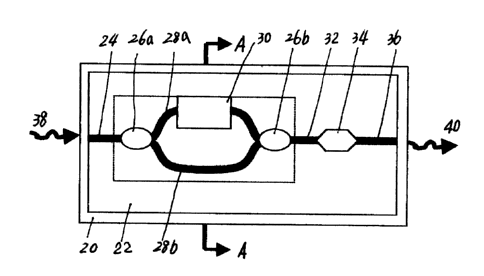
FIG. 1 Configuration of a waveguide variable optical attenuator using the Mach-
Zehnder interferometer configuration and polarization dependence compensator,
where
FIG. 1(a) is the top view, FIG. 1(b) is the cross section along the axis A-A,
and FIG. 1(c)
is the detailed schematic and operation principle of the Mach-Zehnder
interferometers
configuration based on two 3dB couplers.
FIG. 2 Two different connection forms of polarization dependence compensator
for the
waveguide variable optical attenuator, where FIG. 2(a) is based on the bending
waveguides structure and FIG. 2(b) is based on the asymmetric periodic
waveguides
structure.
FIG. 3 Schematic of the Mach-Zehnder interferometer configuration based on two
3dB
Y junctions, other possible option for the variable optical attenuator based
on the current
invention.
FIG. 4 Schematic of the Mach-Zehnder interferometer configuration based on
electro-
optic modulation, the other possible modulation for the variable optical
attenuator based
on the current invention.
Detailed Descriution of the Invention
In this invention, the waveguide Mach-Zehnder interferometer (MZI)
configuration is
used and it contains two 3dB directional couplers connected by two waveguide
arms.
This configuration basically exploits the phase property of the light. The
input light is
split and sent to two separate waveguide arms by the first 3dB directional
coupler, then
combined and split one last time by the second 3dB directional coupler. One or
two of the
waveguide arms are modulated to produce a difference of optical path length
between
these two waveguide arms. The modulating means can be either thermo-optic (TO)
or
electro-optic (E0). If these two optical paths are the same length, light
chooses one exit,
and if they have a difference it chooses the other. As a 2x2 switch, two input
ports and
two output ports are needed and this phase difference is ~, so that the
optical signals can
have two exits and each exit can have two output states of high and low. But,
as a
CA 02368161 2002-O1-16
variable optical attenuator, only the input end where the light is launched
and the output
exit that the light chooses are needed and this phase change can be any value
with respect
to the desirable attenuated degree. As either 2x2 switches or variable optical
attenuators,
the isolation between two output ports is important because it directly
determines the
ON/OFF extinction ratio of one output port as 2x2 switches or attenuation
dynamics as
variable optical attenuators. Meanwhile, the isolation is strongly dependent
of the
coupling ratio of the two 3dB directional couplers. Namely, the closer to
50°Io the
coupling ratio of the 3dB directional coupler is, the higher the isolation
between two
outputs at the two exits is, and further the higher ON/OFF extinction ratio
the 2x2 switch
has at each output port. In theory, if the coupling ratio of the 3dB coupler
is exactly 50%
(i.e., -3dB), the isolation between two output ports should be inFnity. In
fact, no perfect
3dB directional coupler exists because the errors in both design and
fabrication,
especially in fabrication, are not avoidable.
As shown in FIG. 1, this waveguide variable optical attenuator comprises a
substrate
20, cladding 22, waveguide of input port 24, two waveguide 3dB couplers 26a,
26b, two
waveguide arms 28a and 28b connecting the two 3dB couplers, and one modulating
electrode 30 (it is also called heater for thermal modulation), a waveguide
channel 32
connecting the exit that the light chooses when no optical phase change
between two
waveguide arms, one polarization dependence compensator (PDC) 34, and a
waveguide
output port 36 connecting the PDC. The MZI configuration is composed of two
3dB
directional couplers 26a and 26b, and two waveguide arms 28a and 28b. The
modulating
electrode 30 is made on one waveguide arm 28a of the MZI configuration to
produce an
optical phase change. In fact, the MZI configuration based on two 3dB couplers
should
have two input ports and two output ports as shown in FIG. 1 (c), so it is
more popularly
used to form a 2x2 optical switch as mentioned above. In this invention, it is
used as a
variable optical attenuator and only one input port 24 where the optical
signal 38 is
launched and one output port 32 that the optical signal 40 chooses are used.
The other
input port 24a is at the idle state or probably useful for reducing the return
loss of the
system and the other output port 32a is used to split the undesirable optical
beam away
during this system is being operated to attenuate the output optical signal
40.
For simplicity, the thermal modulation is taken as an example to describe the
operation
process and the difference between the variable optical attenuator based on
the present
invention and the conventional structure having no polarization dependence
compensator.
As shown in Fig. 1, if an optical signal 38 is launched into the input port
24, it is split into
two parts at 50% coupling ratio by the 3dB directional coupler 26a, then these
two parts
pass through two waveguide arms with the same length 28a and 28b, finally they
are
combined into one optical signal again by the 3dB directional coupler 26b. If
the
electrode 30 is not activated by a modulating signal (at the OFF-state), the
optical signal
is sent into the cross-state waveguide path 32 as an output optical signal of
the MZI
configuration. This optical signal has to pass through a PDC 34 before it is
coming out at
the output port of waveguide 36, so the output optical signal 40 is at the
high output state
for both the TE-mode and the TM-mode. Research shows the polarization of the
optical
beam can be changed when it passes through the two 3dB couplers and these two
3dB
couplers have different coupling efficiencies for the TE-mode and the TM-mode,
so the
output optical signal 40 should have different values for the TE-mode and TM-
mode.
CA 02368161 2002-O1-16
Namely, the output optical signal 411 has polarization dependence, the
experimental
results show the polarization dependence of output optical signals induced by
MZI
configuration is not much if the birefringence of the waveguide material can
be
controlled at a small value. For example, the polarization dependence of MZI
configuration based on silica-on-silicon waveguides is averagely less than
0.3dB, which
basically can be acceptable in the fiber-optical communications industry. For
the same
optical signal 38 launched into the 3dB directional coupler 26a, when the
electrode 30 is
activated by a modulating signal (at the attenuated-state), an optical phase
difference is
produced by this modulating process, the two parts of the optical signal
coming from two
waveguide arms can not be completely combined into one optical signal again
and only
some of optical beam is sent to the waveguide path 32 and the left pqrt of
optical beam is
sent to the other exit 32a of the MZI configuration as shown in Fig. 1(c),
then the output
signal 40 is attenuated some. Namely, the value of output optical signal 40
depends on
the optical phase change induced by the applied modulating process. When the
optical
phase change induced by the modulating process is exactly ~ or the odd times
of ~, the
optical beam will be 100% sent to the other exit 32a and no optical beam can
be sent to
the expected waveguide channel 32, so the value of output optical signal 40 is
theoretically zero. But, in practice the absolute zero output never exists
because the
optical phase change cannot exactly be controlled at the value of ~ and the
coupling
efficiency of two 3dB couplers also has some errors. The attenuated part sent
to the
expected waveguide channel 32 can be practically attenuated to much less than
20dB,
which is referred as attenuation dynamics. What is more important is the
optical phase
change is different for the TE-mode from for the TM-mode at the same
modulating
process, thus the attenuated degree is certainly different for the TE-mode
from for the
TM-mode, and even the difference in the deeply attenuated output of the MZI
configuration based on two 3dB couplers between the TE-mode and the TM-mode is
much higher. Namely, the polarization dependent loss (PDL) of the variable
optical
attenuator with MZI configuration is always a very critical issue in the
product
development. Therefore, in this invention, a PDC 34 is introduced into the
variable
optical attenuator with the MZI configuration. The operation principle of the
PDC 34 is
to produce a polarization rotation of 90° with a ratio of 50% for the
optical beams passing
through it. Namely, the original beam of TE-mode will become a half of TE-mode
and a
half of TM-mode after the optical beam passes through this PDC. This
polarization
rotation effect is the same to the original beam of TM-mode. Therefore, the
output optical
signal 40 will theoretically have the same amount between the TE-mode and the
TM-
mode. Namely, the PDL will be corrected to a much lower value in theory. The
PDC 34
used in this invention can have several different designs including the curved
waveguide
channels, the periodic changed waveguide channels, the asymmetric poling and
so on. In
this invention, two typical designs for the PDC 34: the curved waveguide
channels and
the asymmetric periodic changed waveguide channels are provided for choices as
shown
in Fig. 2(a) and Fig. 2(b), respectively.
As mentioned above, the directional couplers with a coupling ratio of 50%,
called 3dB
directional coupler, are the most useful optical function elements in not only
the 2x2
optical switch, but also the variable optical attenuator based on the current
invention. As
shown in Fig. 1, the MZI configuration consists of two 3d8 directional
couplers and two
CA 02368161 2002-O1-16
waveguide arms of the same length. One of the waveguide arms is deposited with
the
metal electrode (it is also called heater for the thermal modulation, while
for the electrical
modulation, it is called as electrode and two electrodes have to be used). The
PDL comes
from the coupling process of two 3dB couplers during the MZI configuration is
attenuated by a modulation, so we start the analysis with one 3dB coupler at
two different
mode states: the TE and the TM modes. For a 3d8 directional coupler, assuming
the
input optical power Po exactly has O.SPo TE-mode and O.SPo TM-mode, and the
output
powers of the 3dB directional coupler at the TE-mode and the TM-mode are P,TE
and
P,"" , respectively, at the bar-state port and are PTE and PT"' ,
respectively, at the cross-
state port, then the coupling ratio at the two polarization modes kTE and k""
are defined
by
PTE
k~ - PTE + PTE (la)
z
PTM
TM __ )
k P,~" + P~" 1b
In the same manner, the coupling losses at the two polarization modes L~E and
Lc"' of the
3dB directional coupler are defined by
L~E = l O logio ( l,~ ~+PprE ) (2a)
L~ =101og1o ( P"o.+PP~ ) (2b)
i
As well known, the same thermal (or electrical) modulation can produce
different change
of refractive index. Assuming the changes of refractive index of waveguide
produced by
the modulation are OreTE and tlnTM for the TE-mode and the TM-mode,
respectively, and
the corresponding phase differences between two waveguide arms of the MZI
configuration for the two polarization modes should be
TE
e~TE _ 2~.~1
Y' ~ (3a)
~~Ti" ' 2~L~rc (3b)
CA 02368161 2002-O1-16
where L is the length of the modulated waveguide (i.e., the length of the
electrode) and
~, is wavelength. For the TO modulation, OrcTE and OnTM are related to the
temperature
change OT by the TO coefficients dn~ l dT and dn"" l dT of the waveguide
material as
TE dnTE
dT ~T (4a)
OrcTM - daT OT (4b)
and for the EO modulation, ~rzTE and ~rcTM are related to the applied
electrical field E
by the EO coefficient r33 of the waveguide material as
OnTE - - ~ r33nTE E (5a)
~~ - - 2 rs3nM E (5b)
where n,.E and n,.~ are the refractive indices of the EO waveguide material
for the TE-
mode and the TM-mode, respectively. Then two output efficiencies of the MZI
configuration for the variable optical attenuator based on the current
invention at the TE-
mode and the TM-mode are
~TE
ATE = 4kTE (1- kTE ) cos z ( 2 ) (6a)
Q ~TM
ATM = 4kTM (1- kTM )cost( Y'2 ) (6b)
In terms of the definition of the PDL of the communication components, without
the
PDC, the PDL of the variable optical attenuator based on the current invention
at any
state can be defined by
TE
PDL =1 loglo ( ~~ ) (7)
Because kTE and kT"'' indicate the coupling ratios of the 3d8 couplers in this
regime at
the TE-mode and the TM-mode, respectively, and ATE and ATM indicate the
optical phase
changes between two waveguide arms in this regime for the TE-mode and the TM-
mode,
respectively, the PDL can be existing in both the unattenuated and the
attenuated states,
and it is also a function of the optical phase changes (i.e., the attenuated
depth) even
CA 02368161 2002-O1-16
when the polarization dependence of the 3dB couplers is reduced to be zero
(i.e., kTE -
kT"' ). As described above, a PDC, which typically has two designs as shown in
Fig. 2(a)
and Fig. 2(b), respectively, is introduced in this variable optical
attenuator. It can make
the polarization state of the optical beams rotate 90° with 50% ratio.
Thus, the
polarization states of the two output efficiencies of the MZI configuration
for the variable
optical attenuator based on the current invention defined by the set of
equations (6a) and
(6b) become new states ~N and ~N' as defined by
TE TM
rIN =2(rITE'f'~7~)=2 kTE(1-kTE)cos2(~~ )+kTM(1-kTM)cos2(~~ ) (8a)
TE TM
~7N - 2(~1TE+~7TM)-2 kTE(1 kTE)cOSz(~~ )+kTM(1-kTM)COS2(~~ ) 8b
Thus, with the PDC, the new PDL of the variable optical attenuator based on
the current
invention should be defined by
TE
PDLN =1 loglo ( ~ M ) = 0 (9)
rIN
The result defined by Eq. (9) is based on the theoretical state, but the
polarization rotation
ratio of a practical PDC cannot be exactly 50%, some designed and fabricated
errors are
not avoidable, so the practical value of PDLN could not be exactly zero like
Eq. (9). But,
it can be reduced to an acceptable value with the introduction of the PDC.
Therefore, two
paramount parameters, the PDL and the system loss of the variable optical
attenuators
based on the current invention can be directly improved much better than any
conventional structure, which is exactly the main goals of the current
invention. In this
invention, the MZI configuration is based on two 3dB couplers in order to
obtain a low
system loss. It, however, can be also based on two Y junctions as shown in
Fig. 3 where
the system loss will be relatively high. In addition, the schematic structure
shown in Fig.
1 is based on the thermo-optic modulation. In fact, as mentioned in the
context, this
device is also based on the electro-optic modulation as shown in Fig. 4 where
two
electrodes are used as cathode and anode and labeled as 30a and 30b,
respectively.
Finally some useful papers for understanding the operation principle of "the
PDC"
based on the polarization rotation are the following:
~ Polarization rotation in semiconductor bending waveguides: a coupled-mode
theory by Liu, et al., Journal of Lightwave Technology, Vol. 16, No. 5, May
1998, pp. 929-936;
~ Novel compact polarization converters based on ultra short bends by Dam, et
al.,
IEEE Photonics Technology Letters, Vol. 8, No. 10, October 1996, pp. 1346-
1348.
CA 02368161 2002-O1-16
~ First realixed polarization converter based on hybrid supermades by Mertens,
et
al., IEEE Fhotonics Technology Letters, Vol. 10, No. 3, March 1998, pp. 388-
390.
~ Polarization rotation in asymmetric periodic loaded rib waveguides by Shani,
et
al., Applied Physics Letters, Vol. 59, No. 11, September 1991, pp. 1278-1280.