Note: Descriptions are shown in the official language in which they were submitted.
CA 02368384 2010-10-06
WO 01/62433 PCT/JPO1/01359
pE5 .RI P OO
A CONTROL METHOD FOR COPPER DENSITY IN A SOLDER DIPPING BATH
BACKGROUND OF THE INVENTION
1. Field of the invention
The present invention relates to a composition of a lead-free
solder, and more particularly, to a method for controlling the
composition of a molten solder alloy in a solder bath to manufacture
appropriate solder joints in a solder dipping operation.
2. Description of the Related Art
Solder typically acquires its wettability on metals at a
relatively low temperature of 2501 (degrees centigrade) or so.
When a printed board or lead wires are made of copper, copper on
the surface of the component dissolves into a -solder bath in a
soldering operation. This is called copper leaching. In lead-free
solder, copper quickly dissolves during the wetting. The inventors
of this invention have learned that the copper density rapidly rises
in a solder bath. With the copper density rising, the melting point
of the solder rises, surface tension and flowability change, leading
to solder bridges, voids, incomplete solder connections, solder
spikes, icicles, etc. The quality of the solder joint is thus
substantially degraded. Further, in association with the copper
density rise, the melting point rises. Once started, the rising of the
copper density increases along with the rising of the melting point.
One of the inventors of this invention have developed a novel
CA 02368384 2001-09-26
WO 01/62433 PCT/JP01/01359
2
solder alloy containing nickel (International Publication
W099/48639), and have successfully improved flowability with
nickel adding in the disclosed technique. In this case, the proper
control of the content of copper is desirable.
Once the copper density rises, replacing the entire solder in a
bath with new solder is an effective means to resolve this problem.
The replacement of the solder, however, needs to be frequently
performed, increasing costs, and requiring needless disposal of
resources.
SUMMARY OF THE INVENTION
The present invention has been developed to resolve the
above problem. It is an object of the present invention to provide
a control method for controlling the copper density within a proper
range without the need for the replacement of solder in a bath.
When widely used copper-plated printed boards and
component parts having copper lead wires undergo a dip soldering
operation, the copper density in the molten solder in a bath rises as
a result of copper leaching. Learning that it is impossible to
prevent this phenomenon, we have concluded that positively
controlling the copper density by diluting the copper content is the
best way possible.
Among solder alloys containing copper as the essential
composition thereof, a Tin-Copper-Nickel based alloy, for example,
is produced to improve solderability by adding a small amount of
nickel to a Tin-Copper eutectic alloy, which are basic compositions
CA 02368384 2001-09-26
WO 01/62433 PCT/JP01/01359
3
for a lead-free solder. When dissolved, this solder exhibits an
excellent flowability, and has high dip soldering performance in the
assembly of a large quantity of electronic boards. This solder is
almost free from bridges, voids, incomplete solder connections,
solder spikes, icicles, etc. which are always problematic in a
volume production. However, there is a substantial increase in the
copper density of the molten solder in the bath depending on the
throughput of the bath. The copper leaching develops a Tin-
Copper intermetalic compound having a high melting point and
unable to be dissolved at a predetermined operating temperature.
We have observed that the alloy sticks on an object to be soldered,
thereby degrading the solder quality. The amount of copper
dissolved in tin varies with temperature. Since copper has a high
melting point of 1,083 C , even a slight increase of copper results in
a substantial rise in the melting point of the solder. We have
studied ways of continuing the soldering operation without
increasing the copper density in the solder, and developed the
following method.
When a rise in the copper density of the molten solder in a
bath containing tin, nickel and copper as the major compositions
thereof, is observed, an alloy containing at least tin and nickel and
further no copper at all or a copper content having a density lower
than that of an initial molten solder held in the bath is replenished.
When a lead-free solder of about 0.5% copper, and about 0.05%
nickel with balanced tin as a reminder is introduced into a bath, an
alloy containing at least about 0.05% nickel with balanced tin or an
CA 02368384 2001-09-26
WO 01/62433 PCT/JP01/01359
4
alloy containing at least about 0.05% nickel with balanced tin
including less than 0.5% copper is replenished in order to keep
solder conditions good with the replenishment of copper.
In another example, a lead-free solder of about 0.8% copper,
about 3.5% silver, and about 0.05% nickel with balanced tin is
introduced into a solder bath, an alloy containing at least about
3.5% silver, and about 0.05% nickel with balanced tin, or an alloy
containing at least about 3.5% silver, and about 0.05% nickel with
balanced tin including less than 0.8% copper is replenished in order
to keep solder conditions good.
Since an alloy to be replenished (hereinafter "replenished
alloy") has no copper content at all or a copper content having a
density lower than that of the molten solder alloy prior to the alloy
replenishment, the copper in the bath is diluted when the
replenished alloy dissolves in the bath. Although the addition of
copper in the replenished solder is not a requirement, when an
increase rate in the copper density is slower than expected
depending on the temperature conditions in the solder bath, it may
be better to add a little amount of copper. The solder may be
greatly consumed, for example, by a printed board having through-
holes. In such a case, the replenishment of an alloy having no
copper content at all is expected to excessively lower the copper
content, and the replenishment of the alloy containing a slight
amount of copper is preferable.
The lead-free solder in the bath includes tin, copper, and
nickel. The present invention is not limited this. The present
CA 02368384 2001-09-26
WO 01/62433 PCT/JP01/01359
invention may be applied as long as the solder alloy in the bath
includes at least copper. The present invention is also applied
when the solder alloy in the bath includes elements for improving
wettability or for anti-oxidation. To this end, silver, bismuth,
5 indium, phosphorus, germanium, etc., may be included in the solder
alloy. This means also falls within the scope of the present
invention.
The amount of replenished solder is determined considering
the consumption of molten solder in a bath, liquidus temperature,
solder consumption per batch of printed boards, etc. In many
cases, an increase in the copper density and the throughput of the
printed boards are linearly correlated. The level of the molten
solder in the bath is continuously monitored. The solder is then
replenished when the amount of the solder drops below a
predetermined level. The shapes of replenished solder bulk
include but are not limited to a solder bar or a solder wire. Since
the increase in the copper density and the throughput of the printed
boards are linearly correlated as already discussed, a predetermined
weight of solder may be replenished in response to a predetermined
throughput of printed boards. Alternatively, solder replenishment
may be performed for a predetermined period of time. These
methods, optionally, may be used in combination.
In an optimum control to resolve various problems involved
in the copper density rise, the copper density of the molten solder
containing tin, copper and nickel as the major compositions thereof
is preferably kept to less than 0.85 weight % with the molten solder
CA 02368384 2001-09-26
WO 01/62433 PCT/JP01/01359
6
at a temperature of about 255 C . A density target of 0.85 weight %
is not a strict value but an approximate value, and has a margin
depending on a shift in liquidus temperature. However, as solder
connections become degraded over 0.90 weight %, the copper
density target of 0.85 weight % may be observed, in this sense.
An apparatus, incorporating a printed board that is
manufactured through the dip solder bath controlled in accordance
with the above method, substantially prevents introduction of lead,
which is considered as a poisonous metal. The apparatus does not
contaminate working environments during manufacturing, and
presents no serious environmental problems when it is disposed.
BRIEF DESCRIPTION OF THE DRAWINGS
FIG. 1 is a graph plotting a change in a copper density in the
conventional art; and
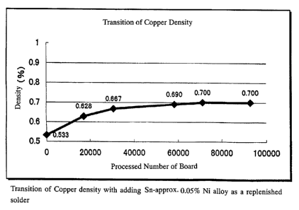
FIG. 2 is a graph plotting a change in a copper density when a
solder containing Sn-0.05%Ni is replenished.
DESCRIPTION OF THE PREFERED EMBODIMENTS
Comparative examples;
A solder bath was filled with a solder containing about 0.5%
copper, and about 0.05% nickel with the balanced tin. A great deal
of printed boards was processed at a solder temperature of 255 2 C .
When solder having the same composition as the initial solder was
continuously replenished, the copper density in the bath increased
to an undesirable level as shown in FIG. 1 in excess of an output of
CA 02368384 2001-09-26
WO 01/62433 PCT/JP01/01359
7
20000 printed boards. As a result, the melting point of the solder
in the bath rises, the solder in the bath changes in surface tension
and flowability. Solderability of the solder became extremely poor
with solder bridges, voids, incomplete solder joints, solder spikes,
icicles, etc. Percentage hereinafter is expressed in weight
percent throughout.
Example 1 of this invention;
A solder bath was filled with a lead-free solder containing
about 0.5% copper, and about 0.05% nickel and balanced tin. A
great deal of printed boards was processed at a solder temperature
of 255 2C under the same conditions as those in the comparative
example. Solder having no copper content at all was then
replenished. In this example, the replenished solder containing
about 0.05% nickel with the remainder tin was continuously added.
The copper density was stable at a level of 0.7% or so as shown in
FIG. 2. No poor soldering performance was created.
Example 2 of this invention;
A solder bath was filled with an initial solder alloy containing
about 0.6% copper, about 0.05% nickel with an antioxidant metal
such as germanium, phosphorus or calcium added in a proper
amount and with the remainder tin. A soldering operation was
performed at a solder temperature of 255 2cC under the same
conditions as those in the comparative example. A solder alloy
identical to the initial solder alloy in the bath, but without copper,
CA 02368384 2001-09-26
WO 01/62433 PCT/JP01/01359
8
was replenished. As a result, like in the example 2, the copper
density reached about 0.7% and flattened off and was stabilized at
that level.
Example 3 of this invention;
A solder bath was filled with a lead-free solder containing
about 0.6% copper, and about 0.05% nickel with the remainder tin.
A soldering operation was performed at a solder temperature of 255
2 C under the same conditions as those in the preceding
examples. A Tin-Nickel solder without copper but with an
antioxidant metal such as germanium, phosphorus or calcium added
in a proper amount was replenished. As a result, like in the above
examples, the copper density reached about 0.7% and flattened off
and is stabilized at that level.
The solder alloys used were a Tin-Copper-Nickel alloy.
Positively controlled element was only copper, and there is no need
for controlling other elements. This is true of the alloys which
contain silver, bismuth, indium, phosphorus, germanium, etc. for
improving wettability or for anti-oxidation.
The present invention positively controls, in a molten solder
in a bath, copper which is an essentially required metal but is
detrimental to solderability when the density thereof exceeds a
threshold value. Even if a great deal of soldering operations is
performed using the same solder bath, the quality of solder joints is
kept excellent. An apparatus, incorporating a printed board that is
manufactured through the solder dipping bath controlled in
CA 02368384 2001-09-26
WO 01/62433 PCT/JP01/01359
9
accordance with the above method, substantially reduce lead, and
neither contaminate manufacturing environments, and operational
environments, nor emit a large quantity of lead in disposal
operations. The environmental contamination with volume
production is thus substantially controlled.