Note: Descriptions are shown in the official language in which they were submitted.
CA 02368667 2001-09-21
WO 01/57967 PCT/JPO1/00645
DESCRIPTION
CONNECTOR AND METHOD OF MAKING
FIELD OF THE INVENTION
The present invention is directed to a connector and a method of manufacturing
the same, and more specifically, to a connector having an insulating housing
and an
insertable EMI filter through which selected signal transmission members of a
plurality
of signal transmission members extend.
BACKGROUND OF THE INVENTION
Heretofore, in a connector that has an insulating housing and multiple signal
transmission members that are inserted therethrough and whose conductors are
electrically connected to each other, connectors have been used in which
electromagnetic interference (EMI) measures are taken by causing signal
transmission
members to pierce a ferrite core, as shown, for example, with the connector
described in
unexamined utility model Hl-140786 [1989]. In such prior art connectors, it is
normally very difficult to form the housing and ferrite core by integral
molding, so they
are each manufactured separately, and during assembly the ferrite core is
forcibly
inserted into and mounted inside the housing, which makes manufacturing the
connector more complicated.
In another prior art connector, the housing itself is formed by a ferrite
core, and
multiple connector pins that act as signal transmission members are inserted
inside (as
described in examined patent H7-48427 [1995]). With such a prior art
connector, there
is no need to separately provide ferrite pieces or other filter elements, and
a connector
having EMI measures can be made by a simple manufacturing process. Also, such
a
connector is suitable for power source lines in that adequate EMI measures can
be
CA 02368667 2001-09-21
WO 01/57967 PCT/JPO1/00645
applied. However, in such a structure the ferrite core acts as an impedance
element
provided on each connector pin. Therefore if such a connector is used as a
connector
for a DC power source that consists of voltage impression wires and grounding
wires,
the problem arises that a ferrite core will also be provided on the grounding
wire part,
for which no EMI measures actually need to be taken, and because this ferrite
core will
act as an impedance element, a standard electric potential will arise between
conductors
connected by the grounding wires, and it becomes difficult to make uniform the
standard electric potentials of all the conductors connected by the grounding
wires.
OBJECTS OF THE INVENTION
It is an object of the present invention, therefore, to provide a connector in
which an EMI filter is arranged according to the electrical signals that flow
along the
signal lines.
It is a further object of the present invention to provide a connector in
which
selected signal transmission members extend through an EMI filter and selected
signal
transmission members do not.
It is a still further object of the present invention to provide a
connector~that can
be manufactured with a drop-insertable EMI filter.
Still other objects and advantages of the invention will become clear upon
review of the following detailed description in conjunction with the appended
drawings.
SUMMARY OF THE INVENTION
A connector is provided with an insulating housing and multiple signal
transmission members that are inserted through said housing. The signal
transmission
members are arranged parallel to a direction that is perpendicular to the
direction in
which they are inserted through said insulating housing, and formed in said
insulating
housing is a core insertion part into which is inserted an EMI filter or a
ferrite core that
CA 02368667 2001-09-21
WO 01/57967 PCT/JPO1/00645
3
is pierced by at least some of the signal transmission members among said
multiple
transmission members. Thus, the signal transmission members that pierce the
ferrite
core may be signal lines along which electrical signals flow, and the signal
transmission
members that do not pierce the ferrite core may be grounding wires or the
like. Thus, it
is possible to prevent the ferrite core from also acting as an impedance
element on the
grounding wires.
A method of manufacturing the connector is also provided, where the EMI filter
or ferrite core may be simply inserted or dropped into the core insertion part
of the
insulating housing, which is easier to manufacture than if the ferrite core
needed to be
forcibly inserted. It is desirable that the cross-section of the core
insertion part be
concave, so that the EMI filter or ferrite core can be easily seated within
such insertion
part. Also, by inserting a plurality of signal transmission members through
the
insulating housing and by causing select transmission lines to pierce the
ferrite core
after the ferrite core has been inserted into the core insertion part, it
becomes possible to
securely fix said ferrite core in its prescribed position, without the ferrite
core becoming
dislodged from the core insertion part.
BRIEF DESCRIPTION OF THE DRAWINGS
FIG. 1 is a perspective view of an entertainment device incorporating the
connector of the invention.
FIG. 2 is a front view of the entertainment device of FIG. 1.
FIG. 3 is a perspective view of the internal structure of the entertainment
device
of FIG. 1.
FIG. 4 is a perspective view showing the back of the entertainment device of
FIG. 1.
FIG. 5 is a cross section taken along line 5-5 in FIG. 3.
FIG. 6 is an enlarged view showing the connector of the present invention.
CA 02368667 2001-09-21
WO 01/57967 PCT/JPO1/00645
4
FIG 7A is a front view, FIG. 7B is a plan view and FIG. 7C is a cross-
sectional
view of the connector of the present invention.
FIG. 8 is an exploded perspective view of the connector of the invention.
DETAILED DESCRIPTION OF THE PREFERRED EMBODIMENTS
The following detailed description is of the best mode or modes of the
invention
presently contemplated. Such description is not intended to be understood in a
limiting
sense, but to be an example of the invention presented solely for illustration
thereof, and
by reference to which in connection with the following description and the
I 0 accompanying drawings one skilled in the art may be advised of the
advantages and
construction of the invention. In the various views of the drawings, like
reference
characters designate like or similar parts.
FIGS. 1 through 5 illustrate an entertainment device I in which is
incorporated
the connector of the invention. Entertainment device 1, for example, might
read a game
program recorded on an optical disk or other medium and executes it according
to
instructions from the users (i.e., game players). "Executing a game" means
mainly
controlling the progress of the game as well as its display and sound.
Entertainment
device 1 has a main body 2 housed inside a cabinet 3. Cabinet 3 has a center
chassis 4,
upper case 5 and lower case 6, and is preferably formed in the shape of a
square on the
plane and in roughly the shape of an "L" in front. The front of lower case 6
are
provided with air intake openings 6A for cooling the interior of device I .
The cabinet 3
is constructed asymmetrically about center chassis 4 (see FIGS. 2 and 5) so
that
entertainment device 1 can be used in either horizontal or vertical
orientation. If used in
the horizontal orientation, the lower surface of lower case 6 contacts the
floor. The left
side surfaces of lower case 6 and upper case 5 are aligned so that the
entertainment
device I can be positioned in the vertical orientation.
CA 02368667 2001-09-21
WO 01/57967 PCT/JPO1/00645
On the front right side of upper case 5 is disk device 11, which controls the
action of a CD-ROM, DVD-ROM, or other optical disk loadable into a disk tray
11B.
On the right side of disk tray 11 B are arranged, on top and bottom, power
switch 16 and
tray operation switch 17 for loading disk tray 11 B into and withdrawing it
from upper
case 5. Provided in the center part of the surface of power switch 16 is a red
LED 71
and a green LED 72, which display the status of power supply to said
entertainment
device 1. The red LED 71 and green LED 72 are unitized such that only one of
them
emits light. Provided in the center part of the surface of tray operation
switch 17 is a
blue LED 73, which displays the operation status of disk device 11.
On the front left side of upper case 5 are two slots 18, each having a memory
card insertion unit 61 positioned at the top and a controller connection unit
62
positioned at the bottom. A memory card or other external auxiliary memory
device is
inserted into insertion hole 61A of memory card insertion unit 61 and shutter
61B is
provided for protecting the connection terminal provided inside. Controller
cormection
unit 62 is an input/output terminal to which is connected a connection
terminal formed
at the end of a controller cable that extends from a controller or operation
means. The
insertion hole 62A of the controller connection is formed approximately in
the~shape of
a rectangle that is long in its horizontal direction, with the lower corners
shaped rounder
than the upper corners, which prevents the connection terminal of the
controller from
being connected in the wrong orientation. Because the shape of insertion hole
62A is
given from insertion hole 61A for memory card insertion unit 61, there is no
danger of
inserting an external auxiliary memory device into insertion hole 62A. Having
two of
these controller connection units 62 makes it possible to connect two
controllers,
allowing two users to play competitive games, etc, and the results of
operating the
controller connected to each controller connection unit 62 are recorded onto
an external
auxiliary memory device inserted into memory card insertion unit 61.
CA 02368667 2001-09-21
WO 01/57967 PCT/JPO1/00645
6
On the front left side of lower case 6 are data transfer terminal 19 and two
external device connection terminals 20. Data transfer terminal 19 conforms to
the
IEEE 1394 standards, and allows connection to a digital camera, video deck or
the like.
The two external device connection terminals 20 conform to USB standards and
allow
connection to external devices such as a keyboard, mouse, printer, an external
memory
device and the like.
As shown in FIG. 4, center chassis 4 has a rear surface part 41 and a middle
shelf 42, which is perpendicular to rear surface part 41 in the height
direction. Rear
surface part 41 consists of upper rear surface part 43, which covers the rear
surface of
cabinet 3 and is long enough to block part of the rear surface of upper case
5, and lower
rear surface part 44, which is long enough to block part of the rear surface
of lower case
6. A notch 43A is formed near the right end edge of upper rear surface part 43
and is
provided with a power supply terminal 32A and a main power switch 32B. A
video/audio output terminal 21 is provided below notch 43A, for outputting
video,
audio and other signals to a television or other display device. An optical
output
terminal 22 is provided next to terminal 21 for outputting digital signals to
external
devices, while a PCMCIA slot 23 having an eject button 23A is provided on the
left side
of the lower rear surface part 44. Exhaust openings 41 A are provided
approximately in
the center of rear surface part 41 through which inside air is expelled.
Middle shelf 42
has approximately the same width and depth as upper case 5 and is provided at
right
angles at the interface part of upper rear surface part 43 and lower rear
surface part 44.
A notch (not shown) for accommodating exhaust fan 15 is formed in the part of
middle
shelf 42 in a location corresponding to exhaust openings 41A. Arranged on the
side of
exhaust outlet 41 A is a heat sink 54 and slots 18.
As shown in FIGS. 3 and 5, device main body 2 has a disk device 11, power
source unit 12, and a main board 13 on which a calculation and processing
device is
mounted. Disk device 11 and power source unit 12 are arranged on middle shelf
42 and
CA 02368667 2001-09-21
WO 01/57967 PCT/JPO1/00645
7
main board 13 is arranged in the space between middle shelf 42 and lower case
6.
Power source unit 12 has power source circuit board 31 is mounted on middle
shelf 42
of center chassis 4 and power source unit 32 into which electric power is
input from an
external power source. Power source unit 32 has AC inlet 32A and main power
switch
32B, and is connected to power source circuit board 31 via connector 31 B.
Power
source circuit board 31 has approximately half the plane area of middle shelf
42, and
electric power supplied from an external power source is converted to DC
current and to
the prescribed voltage by capacitors, coils, transformers, and other circuit
elements 31A
that make up said power source circuit board 31. Also provided on power source
circuit
board 31 is a guide plate 31 C for directing the flow of cooling air brought
in through
openings 6A and a print pattern (conductors, not shown) of voltage impression
wires.
In this way, power source unit 12 supplies to disk device 11 and boards 13,
etc. the
power that is obtained by power source circuit board 31.
Main board 13 has a control system (not shown) consisting of a CPU 51 and its
peripheral devices, a graphic system (not shown) including an image processing
unit
that forms output images based on signals from CPU 51, a sound system (not
shown)
consisting of audio processing equipment that generates music and sound
effects, etc., a
microprocessor unit (not shown) that is a power control means that controls
the supply
of electric power from power source unit 12 to said control system, graphic
system, and
sound system, etc., an optical disk control unit (not shown) that controls the
optical disk
on which applications programs are recorded, and a communication control unit
(not
shown) controls the input and output, etc. of signals from the controllers by
which
instructions are input from users, signals output to the controllers, and data
from
external auxiliary memory devices that record the settings of video games, etc
is
provided opposite the lower surface of middle shelf 42. The optical disk
controller has
a decoder that decodes the programs and data, etc. that are recorded with, for
example,
an appended error correction code (ECC), and a buffer that speeds up the
reading of
CA 02368667 2001-09-21
WO 01/57967 PCT/JPO1/00645
data from the optical disk by temporarily storing data from disk device 11.
The control
system has CPU 51, a peripheral device control unit that performs interrupt
control and
control of direct memory access (DMA) data transfers, etc., a main memory
device that
consists of RAM and ROM in which are stored programs such as the so-called
operating system. The "main memory" here refers to the memory in which
programs
can be executed. CPU 51, which controls entertainment device 1 as a whole by
executing the operating system, consists of, for example, a 128 bit RISC CPU.
The
graphic system has an image processing device that renders pictures under
drawing
instructions from CPU S1, and a frame buffer in which images rendered by this
image
processing device are stored. The image processing device draws polygons, etc.
to the
frame buffer in accordance with drawing commands from CPU 51, and is able to
draw
up to about 75 million polygons per second. The sound system has an audio
processing
unit that plays background music and sound effects, etc. under instructions
from CPU
51, and a sound buffer in which waveform data, etc. is stored by this audio
processing
unit.
Attached to the top of CPU 51 and the image processing unit is heat conducting
member 52, which is preferably made of high thermal conductivity aluminum. CPU
51,
the image processing unit, and heat conducting member 52 are covered by
shielding
member 53, which is preferably made of metal and consists of flat shielding
part 55,
which comes into contact with the upper surface of heat conducting member 52,
and
side shielding parts 56 extending from both ends of flat shielding part 55 to
the upper
surface of main board 13. Shielding member 53 prevents outside disturbances
such as
noise generated from power source unit 12 from intruding into CPU 51. Provided
on
heat conducting member 52 is a temperature sensor (not shown), which detects
the
temperature of CPU 51 and the image processing unit. The temperature sensor
has a
sensor unit that detects the temperature of heat conducting member 52 and a
signal
conversion unit that converts the detected temperature to a temperature
detection signal,
CA 02368667 2001-09-21
WO 01/57967 PCT/JPO1/00645
9
which is output to the microprocessor unit. The microprocessor unit controls
the supply
of electric power from power source unit 12 to CPU 51 and the image processing
unit of
main board 13 based on temperature abnormality detection signals from said
temperature sensor. Heat sink 54 is provided on the upper surface of the end
of heat
conducting member 52, spans CPU 51 and the image processing unit via heat
conducting member 52 and extends from the upper surface of heat conducting
member
52 to near the top of upper case 5. Thus, as shown in FIG. 5, openings 42B,
SSA are
formed in middle shelf 42 and flat shielding part 55 in positions
corresponding to the
location of heat sink 54.
Electrically connected to the communication control unit is one end of the
slots
18 consisting of controller connection unit 62 and memory card insertion unit
61, as
well as data transfer terminal 19, external device connection terminal 20,
communication terminal 22, and PCMCIA slot 23, etc., by which said
communication
control unit also controls the input and output of signals with external
devices, etc.
connected to and inserted into these terminals, etc.
As shown in FIG. 6, DC electric power transformed to the prescribed voltage by
power source circuit board 31 is supplied to main board 13 through connector
80. One
end of connector 80 is connected to a first cormection 31D attached to the
lower surface
of power source circuit board 31, and the other end is connected to a second
connection
13A attached to main board 13. Provided on first connection 31 D and second
connection 13A are terminals (not shown) that are connected to the print
patterns (not
shown) formed on power source circuit board 31 and on main board 13,
respectively.
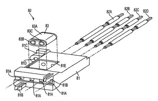
More specifically, as shown in FIGS. 7A-7C and 8, connector 80 comprises an
insulating housing 81 formed by a flexible resin molding, four signal
transmission
members 82A-82D inserted through holes 81 A in housing 81 and electrically
connect
print patterns formed on power source circuit board 31 and on main board 13,
and a
ferrite core 83 provided inside said housing 81. Transmission members 82A-82D
are
CA 02368667 2001-09-21
WO 01/57967 PCT/JPO1/00645
arranged parallel in a direction perpendicular to the direction in which they
are inserted
through insulating housing 81. In order to allow DC electric power to flow
that is
transformed to the prescribed voltage by power source circuit board 31, of the
four
signal transmission members 82A-82D, two signal transmission members 82A, 82B
are
5 made into voltage impression wires on which a DC voltage is impressed, and
the other
two signal transmission members 82C, 82D are made into grounding wires. That
is,
connector 80 is a connector for a DC power source.
The ferrite core 83 is inserted into housing 81 through a concave core
insertion
part 81 E, which is formed by cutting out the side of insulating housing 81.
Formed at
10 one end of insulating housing 81 are hole 81 D and anchoring part 81 C,
whose upper
surface makes contact with the lower surface of middle shelf 42. Two engaging
parts
81 B that engage with second connection 13A are formed on the end face of the
other
end of insulating housing 81 in a position where they form diagonal braces
with signal
transmission members 82A-82D interposed between them. An insertion through-
hole
and a female threaded part (not shown) are formed opposite said hole 81 D of
middle
shelf 42 and power circuit board 31. With them, by inserting a bolt from the
lower
surface side of anchoring part 81 C and screwing said bolt into the female
threaded part
of power circuit board 31, connector 80 is secured to power circuit board 31
via middle
shelf 42.
Ferrite core 83, which is a mufti-layer structure, has outer shell part 83A
and two
insert-through parts 83B, 83C, which are formed inside outer shell part 83A.
Outer
shell 83A is formed in a roughly cylindrical shape whose width is about half
the width
of insulating housing 81, and is inserted into said concave part 81E. Signal
transmission members 82A, 82B, which are inserted through hole 81 A of
insulating
housing 81, pierce these insert-through parts 83B, 83C and are therefore
partitioned one
by one via said insert-through parts 83B, 83C. By causing the two signal
transmission
members 82A, 82B that constitute the voltage impression wires to pierce
ferrite core 83,
CA 02368667 2001-09-21
WO 01/57967 PCT/JPO1/00645
EMI measures are taken on said signal transmission members 82A, 82B. And by
not
interposing ferrite core 83 between signal transmission members 82C, 82D that
constitute the grounding wires, one makes uniform the standard electric
potentials of the
print patterns of the grounding wires formed on power source circuit board 31
and main
S board 13, which are connected by signal transmission members 82C, 82D.
In order to manufacture connector 80, the insulating housing 81 is first
provided
with through-holes 81 A and concave part 81 E. After inserting ferrite core 83
into
concave part 81 E by dropping it in, signal transmission members 82A-82D are
inserted
through insertion through-holes 81 A of said insulating housing 81, with
transmission
members 82A and 82B piercing through parts 83B and 83C of ferrite core 83 and
transmission members 82C and 82D not piercing through ferrite core 83. By
connecting the two ends of connector 80 to first connection 31 D and second
connection
13A, respectively, and causing the two end parts of signal transmission
members 82A-
82D to make contact with such the terminals in such connections, electric
power
transformed to the prescribed voltage by power source circuit board 31 is
supplied to
main board 13. That is, connector 80 is a board-to-board connector in which
main
board 13 and power source circuit board 31 arranged opposite each other are
physically
connected, and print patterns formed on main board 13 and on power source
circuit
board 31 are electrically connected to each other.
Thus, when connector 80 is manufactured, it is easy to just insert ferrite
core 83
into concave part 81E of insulating housing 81, which simplifies manufacturing
of
connector 80 as compared with the prior art. Also, because only certain
transmission
members pierce ferrite core 83, it is possible to take EMI measures only for
the parts on
which a voltage is impressed. That is, by not interposing the ferrite core
between the
grounding wires, ferrite core 83 can be prevented from acting as an impedance
element
on the grounding wires, and by connecting the print patterns of the grounding
wires
CA 02368667 2001-09-21
WO 01/57967 PCT/JPO1/00645
12
formed on main board 13 and on power source circuit board 31, the standard
electric
potentials can be made uniform.
In addition, because insulating housing 81 is formed by a resin molding that
has
flexibility, the insertion of the signal transmission members 82A-82D through
the
housing 81 is easier. Also, because concave part 81E is formed with a concave
cross-
section along the insert-through direction of the signal transmission members,
and the
inside base surface of said concave part 81 E is made the support surface of
inserted
ferrite core 83, said ferrite core 83 can be arranged in its prescribed
position just by
dropping ferrite core 83 into concave part 81 E. In addition, because
anchoring part 81 C
is provided on insulating housing 81, said connector 80 is firmly secured to
power
source circuit board 31, and even if the connection part between power source
circuit
board 31 and connector 80 is subjected to a large vibration, etc., the
connection can hold
firmly without connector 80 becoming loose, thereby making it possible to have
a firm
electrical connection between connector 80 and power source circuit board 31.
Furthermore, the insertion of the signal transmission members through the
ferrite core
acts to fix the ferrite core within the insulated housing and also acts to
stabilize the
entire construction of the connector, thereby making it difficult to break
apart even if
outside force is applied.
While the invention has been described with respect to a preferred embodiment,
alternative constructions are contemplated. For example, while the anchoring
part is
described on the side of power source circuit board 31 of insulating housing
81; it may
also be provided, for example, on the side of main board 13, or it may be
dispensed with
altogether provided that connector 80 does not totter unsteadily even if a
large vibration,
etc. is applied to the connection part between power source circuit board 31
and
connector 80.
In addition, the insulated housing 81 may be provided without the ferrite
core, in
which case all the four signal transmission members exposed and the connector
may be
CA 02368667 2001-09-21
WO 01/57967 PCT/JPO1/00645
13
used even as a connector for an AC power source. Also, the core insertion part
is not
limited to being of concave cross-section, for its shape, etc. may be
determined
appropriately as long as it can accommodate a core which can be pierced by
signal
transmission members. Also, the connector may be used to connect print
patterns or
circuit elements in addition to boards. In addition, the signal transmission
members
may consist of other wires such as voltage impression wires, grounding wires,
and
control signal wires.
While the present invention has been described at some length and with some
particularity with respect to the several described embodiments, it is not
intended that it
should be limited to any such particulars or embodiments or any particular
embodiment,
but it is to be construed~with references to the appended claims so as to
provide the
broadest possible interpretation of such claims in view of the prior art and,
therefore, to
effectively encompass the intended scope of the invention.