Note: Descriptions are shown in the official language in which they were submitted.
CA 02368696 2011-02-15
PROCESSOR BASED STROBE WITH FEEDBACK
Field .of the, Invention:
The invention pertains to strobe lights driven by programmed
processors. More particularly, the invention pertains to such strobes which
respond to
variable input voltages and wherein in-rush currents are limited.
Background of-the Invention:
Circuits for driving strobe lights of a type usable in alarm systems are
known. Some known circuits charge a capacitor using constant frequency,
variable
current signals. Others have incorporated a coil in combination with frequency
varying
circuits. One known system has been disclosed in U.S. Patent No. 5,850,178,
issued
December 15, ,1998, entitled "Synch Module With Pulse Width Modulation" and
assigned to the assignee hereof.
Known circuits have been designed to be driven from a single nominal
voltage such as 12 volts or 24 volts. In addition, known circuits have been
designed
to drive a gas filled tube to produce a single, nominal candela output.
There is- a need for more flexible strobe drive circuitry. Preferably a
single drive circuit could accommodate a range of nominal input voltages. In
addition,
it would be desirable to be able to select from arange of desirable candela
output levels
without regard to available input voltage.
Finally, it would be preferable if in-rush currents could be limited under
various conditions. One known system is disclosed in Ha et al U.S. Patent
6,049,446
assigned to the assignee hereof and entitled,"Alarm Systems and Devices
Incorporating
Current. Limiting Circuit"
Preferably, the above noted features could be implemented so as to
promote manufacturability, and to limit operating in-rush currents. It would
also be
preferable if such flexibility did not appreciably increase unit cost.
Summary of the Invention:.
A. strobe drive circuit combines circuits to accept variable input drive
voltages- with circuitry responsive to selectable candela output levels. In
one aspect,
1
CA 02368696 2002-01-21
the circuitry monitors the time to charge a capacitor to a selected,
predetermined
voltage. In another aspect, the actual capacitor voltage is monitored. A gas
filled tube
can be triggered at the appropriate voltage. Other types of visible output
devices could
also be used.
The charging duty cycle can be varied to respond to various input
voltages as well as differing predetermined flash voltages. The duty cycle of
the drive
current is continually corrected with each flash.
In one embodiment, surge currents are substantially eliminated by
starting with a lower duty cycle and increasing same over time, with each
flash. With
this configuration, power supply fold back or over-current conditions can be
substantially eliminated.
In another aspect, the charging current duty cycle can be incremented
one or more times from an initial value while charging the capacitor.
Simultaneously,
the capacitor's voltage can be monitored. Depending on the results, for
example the
value of the flash voltage of the present flash cycle, the current charging
current duty
cycle can be altered for the next flash cycle.
In another aspect, a current smoothing circuit limits initial turn-on
current for a predetermined interval after power is applied. For example, turn-
on
current can be limited for an interval in a range of 300-700 ms with 500 ms
being a
preferred interval. This is especially advantageous where numerous strobes are
connected to a common power source.
Where synchronization pulses are applied to the drive circuit, for
example from an external source which might be a fire alarm system, capacitor
charging can be interrupted or terminated when such pulses are present. This
will
minimize charge depletion from the capacitor(s).
Where applied energy is in the form of full wave rectified AC, surge
currents can be minimized after each flash by commencing charging (after each
flash)
by waiting till the rectified AC voltage drops to a predetermined low value.
For
example, charging can be commenced once the applied AC drops to about zero
volts.
2
CA 02368696 2002-01-21
A programmed processor can be incorporated into the control circuitry.
Information can be stored relative to a plurality of available candela
outputs. When a
specific output has been selected, corresponding pre-stored information is
used by the
processor to charge the capacitor to the respective output voltage.
In another embodiment, the capacitor voltage can be measured, digitized
in an A/D converter, and compared to a plurality of pre-stored values. In
response to
the comparison step, charging current duty cycle can be altered.
The control process also responds to input voltage variations. With a
lower input voltage, the charge current duty cycle will increase to provide
the
necessary capacitor voltage. With a larger input voltage, the duty cycle will
decrease.
A control method includes the steps of establishing a plurality of target
pulse widths based on respective candela outputs; selecting a candela output
level;
charging an energy source until either a selected voltage is reached or until
a
predetermined time interval has ended; keeping track of the actual charging
time
interval; comparing the actual charging time interval to the target pulse
width
associated with the selected candela output; where the actual time interval is
less than
the target pulse width, decreasing the charging parameter a selected amount
and where
the actual time interval is greater than the target pulse width, increasing
the charging
parameter.
Where the selected voltage is repetitively reached before the
predetermined time interval has ended, the charging parameter can be
repetitively
reduced. This reduction can be via a decreasing amount. Where the
predetermined
time interval repetitively ends before the selected voltage has been reached,
the
charging parameter can be repetitively increased.
In another embodiment, capacitor voltage can be digitized and
compared to a candela specific target value. Depending on the results of this
comparison, charging duty cycle can be altered.
In either embodiment, the closed loop control system responds to
variations in input voltage. Charging duty cycle is adjusted in response
thereto to
3
CA 02368696 2002-01-21
maintain a selected candela output level. Variations in the input voltage in a
range on
the order of 4:1 can be accommodated.
Desired candela output level can be manually set at a unit. Alternately,
it can be downloaded to a unit, as a programmable parameter, from a remote
source.
Numerous other advantages and features of the present invention will
become readily apparent from the following detailed description of the
invention and
the embodiments thereof, from the claims and from the accompanying drawings.
Brief Description of the Drawings:
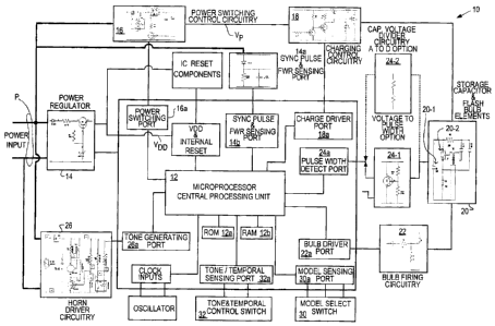
Fig. 1 is a block diagram of a system, having two feedback options, in
accordance with the present invention;
Fig. 1A is a flow diagram which illustrates over-all processing in a
system as in Fig. 1;
Fig. 2A-1 is an overall flow diagram of a method illustrating one form
of operation of the system of Fig. 1;
Fig. 2A-2 is an over-all flow diagram of a method illustrating an
alternate form of operating the system of Fig. 1;
Fig. 2B is a flow diagram illustrating additional details of the methods
of Figs. 2A-1 and 2A-2;
Fig. 3 is a flow diagram illustrating selection of an adjustment routine;
Fig. 4-1 is a flow diagram illustrating a candela adjustment process in
accordance with the method of Fig. 2A-1;
Fig. 4-2 is a flow diagram illustrating a candela adjustment process in
accordance with the method of Fig. 2A-2;
Figs 5-1, 5-2, and 5-3 are timing diagrams which taken together
illustrate candela target searching for raising a bulb voltage to a target
voltage in
accordance with the method of Fig. 2A-1;
Figs 6-1, 6-2, 6-3 are timing diagrams which taken together illustrate
candela target searching for lowering a bulb voltage to a target voltage in
accordance
with the method of Fig. 2A- 1;
4
CA 02368696 2002-01-21
Figs. 7-1, 7-2, are timing diagrams which taken together illustrate
candela target searching for raising a bulb voltage to a target voltage in
accordance
with the method of Fig. 2A-2;
Figs. 8-1, 8-2 are timing diagrams which taken together illustrate
candela target searching for lowering a bulb voltage to a target voltage in
accordance
with the method of Fig. 2A-2;
Fig. 9 is a series of graphs illustrating flash bulb voltage plotted against
on-time for charging the bulb capacitor;
Fig. 10 illustrates additional aspects of the methods of figs. 2A-1, -2;
Fig. 11 is a block diagram of a system in accordance with the invention;
Fig. 12-1, -2, -3, -4 are graphs illustrating capacitor charging in response
to an applied DC signal with synchronizing pulses;
Figs. 13-1, -2, -3, -4 illustrate capacitor charging in the presence of two
relatively close together control pulses;
Fig. 14-1, -2, -3, -4 are graphs of incrementally increasing capacitor
charging in response to full wave rectified AC applied power in the presence
of two
relatively close together control signals;
Figs. 15-1, -2, -3, -4 are graphs of charging processes in response to
relatively close together drop-out control pulses;
Figs. 16-1, -2, -3 illustrate operation of a regulator without a smoothing
capacitor in the presence of applied energy;
Figs. 16-4, -5, -6 illustrate operation of a regulator with a start-up
smoothing capacitor;
Fig. 17 is a schematic of power switching and control circuitry
illustrating use of a turn-on current limiting resistor; and
Figs. 18A-C illustrate operation of the circuit of Fig. 17.
Detailed Description of the Preferred Embodiments:
While this invention is susceptible of embodiment in many different
forms, there are shown in the drawing and will be described herein in detail
specific
5
CA 02368696 2002-01-21
embodiments thereof with the understanding that the present disclosure is to
be
considered as an exemplification of the principles of the invention and is not
intended
to limit the invention to the specific embodiments illustrated.
Fig. 1 illustrates a block diagram of two embodiments of a system 10,
a multi-candela visual output device. The system 10 includes a control
element, for
example a programmable processor, 12.
The processor 12 is coupled to a read-only or programmable read-only
memory 12a and read/write memory 12b. Memory units 12a, 12b can store
executable instructions for carrying out methods discussed subsequently as
well as
parameters and results of on-going calculations.
A power regulator 14 is coupled to power input lines P. Exemplary
circuitry, as would be understood by those of skill in the art, is illustrated
in various of
the circuit blocks, such as circuit block 14. The operation of regulator 14 is
discussed
subsequently with respect to Figs. 16-4, -5, -6.
Lines P provide electrical energy, synchronization pulses and additional
control pulses. Lines P can be coupled to a fire alarm control unit or other
control
devices.
The voltage on the lines P can vary, for example, between 6-40 volts
DC. The principles of the present invention can be used with other ranges of
input
voltages and can be used with half wave or full wave rectified AC input
voltages in a
range of 6-33 volts RMS without departing from the spirit and scope of the
present
invention. Synchronization and/or control pulses present in applied DC or
rectified AC
can be in the form of down-going transitions to, for example, zero volts.
Other forms
of embedded synchronization or control pulses come within the spirit and scope
of the
present invention.
As discussed below, system 10 automatically adjusts to various input
voltages. By way of example, it can be powered without any changes from 12
volts
DC or 12 volts FWR, 24 volts DC or 24 volts FWR.
6
CA 02368696 2002-01-21
Power control circuitry 16 is coupled to lines P and to charging control
circuitry 18. Operation of power control circuitry 16 is discussed
subsequently with
respect to Figs. 17 and 18 A-C.
Processor 12 is coupled to circuitry 16 via port 16a and to charging
control circuitry 18 via port 18a. Processor 12 is coupled to regulator 14 via
sync pulse
and sensing circuits 14a and sensing port 14b.
The charging control circuit 18 is coupled to circuits 20 which include
capacitor 20-1 and flash bulb or tube 20-2 and provides electrical energy to
charge the
capacitor therein using, for example either a variable or a constant
frequency, variable
duty cycle signal. Bulb firing circuitry 22 is coupled via driver port 22a to
processor
12. Where the capacitor in element 20 has been charged to a predetermined
value,
based on selected candela output, the processor 12 can trigger, or flash the
bulb via port
22a.
In one embodiment, voltage to pulse width feedback circuitry 24-1
provides feedback, in the form of a down-going voltage, to processor 12 which
indicates that the voltage across the capacitor, element 20-1, has reached a
predetermined value. This is a value which is independent of selected candela
output.
As discussed subsequently, this feedback signal, could be coupled to processor
12 via
port 24a, can be used to adjust a charging current duty cycle via control
circuitry 18.
In a second embodiment, an analog-to-digital converter, integral to
processor 12 or as a separate circuit, can convert flash bulb or tube voltage
across
capacitor 20-1, reduced by divider circuit 24-2, to a digital value. This
digital, capacitor
voltage value can be compared to a candela related target value, selected by
switch 30,
and the results thereof used to adjust a charge current duty cycle.
Horn driver circuit 26, via port 26a is coupled to processor 12 and
enables the processor 12 to drive an audible output device in accordance with
a
preselected tonal pattern. The pattern can be synchronized by synchronizing
signals
received at port 14b.
7
CA 02368696 2002-01-21
Model select register or switch 30, via port 30a is coupled to processor
12. Switch register 30 can be set, locally or remotely to specify one of
several
available candela outputs, such as 15, 30 or others of interest. Processor 12
can, in
response to a signal(s) from register or switch 30 specifying a selected
candela output,
and, electrical energy of various voltages applied to regulator 14 and power
control 16,
charge capacitor 20-1 to a voltage which when tube 20-2 is flashed or fired
produces
the selected candela output.
Temporal control switch 32 can be set to select an audible tonal output
pattern. Switch 32 is coupled to processor 12 via port 32a.
Fig. 1 A illustrates in over-all form processing carried out by processor
12. Interrupt processing steps 302, 304 phases 1, 2 are carried out by
processor 12
where pulse width feedback, circuits 24-1 and 24a have been implemented.
Details of
phase 2 processing, step 304, are discussed subsequently with respect to Figs.
2A-1,
2B and Fig. 4-1.
Interrupt processing steps 312, 314 phases 1, 2 are carried out by
processor 12 where analog-to-digital feedback, circuits 24-2, 24a have been
implemented. Details of phase 2 processing, step 314 are discussed
subsequently with
respect to Figs. 2A-2, 2B and Fig. 4-2.
Figs. 2A-1 and 2A-2 illustrate two different control processes 90, 92 in
accordance with the present invention. Those of skill will understand that the
processes
are periodic. An exemplary one second cycle is disclosed and discussed, see
Fig. 10.
It will be understood that other periods or cyclic intervals could be used
without
departing from the spirit and scope of the present invention.
Fig. 2A-I illustrates steps of a method 90 of operating system 10 using
feedback circuit 24-1. In an initial step 100 a capacitor charging sequence is
started.
In step 102, circuitry 24-1, via port 24a is checked. If low, the capacitor
voltage has
reached a predetermined value (the same for all candela output). If low, in
step 104,
the feedback signal time to transition from high to low is compared to a
target value.
8
CA 02368696 2002-01-21
In a step 106 if the feedback transition time interval exceeds the target
parameter, the capacitor is not being charged quickly enough and the duty
cycle for
charging the capacitor is increased in a step 108. If the feedback transition
time
interval is less than the target parameter, the capacitor is being charged to
quickly and
the duty cycle for charging the capacitor is decreased in a step 110.
Subsequently, in
step 112 the tube, element 20-2, is flashed.
If the feedback signal from circuit 24-1 is high in step 102, in step 114,
feedback signal time to transition is compared to a maximum interval of .75
second.
If at the limit, in a step 116, duty cycle is increased a maximum amount based
on
selected candela output.
In summary, with respect to process 90:
1. When a specific candela is selected, the executable
instructions assign a target pulse width value (discussed
in more detail subsequently, Fig. 5-2 and 6-2). As each
flash occurs, the conversion for bulb voltage to pulse
width begins. After the conversion is complete, the
result is used to compare to the target pulse width value.
2. If the result pulse width value is more than the target
value, the charging on duty value will increase. This
increase in the duty cycle causes the charging to
increase and as a result, the pulse width decreases. The
amount of duty cycle increase depends on how far the
actual pulse width is from the target. The further away
the target pulse width is, the more the increase will be
applied to charging.
3. The opposite of step 2, above, occurs if the result pulse
width value is smaller than the target value. The duty
cycle will now decrease to slow down the rate of the
charging.
9
CA 02368696 2002-01-21
The charging adjustment continues at each flash until the final target
value is reached and dynamically adjusts the duty value in order to keep the
pulse
width equal to the target value. The process of reaching the target pulse
width allows
the system to track any input voltage in the specified range for that candela,
discussed
in more detail subsequently, see Fig. 9.
One exemplary flash interval is on the order of one second. Other flash
intervals can also be used without departing from the spirit and scope of the
present
invention.
Fig. 2A-2 illustrates an alternate process 92 which uses divider circuitry
24-2 and an associated analog-to-digital converter. A charging sequence is
initiated in
the step 100.
The feedback value, via circuits 24-2 is read and converted, step 101.
The digitized value is compared to a pre-stored target value, step 103.
If the feedback voltage has not exceeded the target value, step 105, a
comparison is made in step 107 to a flash interval, for example a one second
interval,
and if appropriate the tube is flashed in step 109.
If the feedback voltage is less than the target value, step 111, the duty
cycle is increased, step 113. If not, it is decreased, step 115. Bulb voltage
is compared
to a maximum in a step 117. If too large, the capacitor can be discharged.
Fig. 2B illustrates additional aspects of the steps of the method 90 of
Fig. 2A-1 and of alternate process 92, Fig. 2A-2. Fig. 10 illustrates
additional details
of processes 90,92 on a per-cycle basis.
With respect to process 90, in step 120 the timer is initialized. Ina step
122 it is incremented. In a step 124 the feedback signal, from element 24 is
evaluated.
If high, the target voltage has not net been reached and the contents of the
timer are
compared in a step 126 to .75 seconds. If less than or equal, the process
returns to step
122. If not, the process exits, step 128, and duty cycle adjust routine is
initiated, see
Fig. 3. Where the pulse width port indicates in step 124 that the capacitor is
exhibiting
CA 02368696 2002-01-21
a predetermined voltage, if the timer contents are non-zero the duty adjust
routine of
Fig. 3 is initiated step 128.
With respect to process 92, if the time equals or exceeds .9 seconds, step
119, an analog-to-digital conversion takes place, step 121. The duty cycle
adjust
routine, Fig. 3, is then entered.
In steps 123, 125, an analog-to-digital conversion takes place multiple
times in each charging cycle at preset time intervals. In the absence of a
detected over-
voltage condition, step 127, the sample time of the latest voltage value is
compared to
the latest possible sample time for each cycle, step 107, to determine if a
flash cycle
should be initiated.
In summary, with respect to process 92:
1. When a specific candela is selected, the executable
instructions assign a target bulb voltage (see #60, Fig.
7-1 and 8-1). As each flash occurs, the conversion for
bulb voltage to pulse width begins. after the conversion
is complete, the result is used to compare to the target
pulse width value.
2. If the result bulb voltage value is more than the target
value, the charging on duty value will increase. This
increase in the duty cycle causes the charging to
increase and as a result, the bulb voltage increases. The
amount of duty cycle increase depends on how far the
actual bulb voltage is from the target. The further away
the target bulb voltage is, the more the increase will be
applied to charging.
3. The opposite of step 2 above, occurs if the result bulb
voltage value is smaller than the target value. The duty
cycle will now decrease to slow down the rate of the
charging.
11
CA 02368696 2002-01-21
9 6
The charging adjustment continues at each flash until the final target
value is reached and dynamically adjusts the duty value in order to keep the
bulb
voltage equal to the target value. The process of reaching the target bulb
voltage
allows the system to track any input voltage in the specified range for that
candela.
The capacitor voltage is continuously monitored with the A to D to
prevent overcharging. In the event that the capacitor voltage is greater than
the target
value, the charging will be stopped until the voltage drops below the target.
The duty
cycle will be adjusted at the beginning of the next charge cycle.
Fig. 3 illustrates evaluating the selected candela output specified, for
example by setting switch 30, in step 132. The respective target pulse width
is
retrieved from storage units 12a,b step 134-1 or the respective target bulb
voltage is
retrieved from storage, step 134-2. Alternately, in step 134-3 a selected
target bulb
voltage is sensed off of a variable voltage source, for example, a resistor
voltage
divider circuit. The respective adjustment routine is then entered in one of
Figs. 4-1
and 4-2.
Fig. 4-1 illustrates steps 140 in adjusting the capacitor charging duty
cycle parameter for respective settings of candela output where pulse width
feedback
circuitry 24-1, process 90, has been implemented. Fig. 4-2 illustrates steps
in adjusting
capacitor duty cycle for respective settings of candela output where analog-to-
digital
converter, process 92 has been implemented. It will be understood that model
selection
can also take place electronically, perhaps via a message received via power
lines P in
addition to or as an alternate to a locally settable switch or element.
In Fig 4-1 in step 142 the contents of the timer buffer are compared to
a maximum allowed time, such as .75 sec. If they exceed the threshold, in step
144 the
duty cycle is increased by a maximum increment, for example 20 microseconds.
In step 146, substep 146a is a calculation to establish 88% of the current
duty cycle. In step 146b 94% of the current duty cycle is determined. These
two values
are used in the next cycle, illustrated in Fig. 10, to ramp up the charging
current from
a minimal value, to a full 100% value. Step 148 is an exit to the flash
routine. Other
12
CA 02368696 2002-01-21
values could be used without departing from the spirit and scope of the
present
invention.
Steps 150a address a condition where the contents of the timer buffer
exceed the target pulse width parameter for the respective candela value.
Steps 150b
address a condition where the contents of the timer buffer are less than the
target pulse
width parameter for that candela value.
With respect to steps 150a and timing diagrams of Figs. 5-1 to 5-3, in
steps 150a-1,-2 the degree to which the pulse count exceeds the target pulse
count is
determined. As illustrated in Fig. 5-2, the duty cycle of the charging current
should be
increased to accelerate the increase of voltage on the capacitor. The duty
cycle increase
takes place immediately, see Fig. 5-3. The capacitor continues to charge and
one second
after the last trigger signal, the next trigger signal is issued by the
processor 12, via
circuitry 22 irrespective of the then capacitor voltage value, by the flash
routine, step
148.
At the start of the next cycle, charging of the capacitor is initiated at 88%
of the duty cycle, step 146a (see also Fig. 10). Subsequently after a selected
time
interval, as would be understood by those of skill in the art, the charging
rate in
increased to 94% of the duty cycle, step 146b. Then the charging rate is
increased to
100% of the duty cycle, Fig. 5-3.
With a one second flash period, Fig. 5-1, the capacitor could be charged
at the 88% and 94% levels for 15 milliseconds. Other time intervals could be
used
without departing from the spirit and scope of the present invention.
Once the capacitor has been discharged a surge of current may result
when trying to recharge it. By starting each charge cycle, after a discharge,
at a lower
rate and increasing the current (by increasing the percent of the duty cycle)
overcurrent
or surge current problems can be minimized. This process minimizes power
supply
fold-back or shut down problems.
Steps 150b, and Figs. 6-1 to 6-3, illustrate the operation of system 10
where the value of the target pulse width exceeds the contents of the pulse
width timer.
13
CA 02368696 2002-01-21
In this circumstance, the voltage across the capacitor has crossed the
threshold before
the .75 second interval. As illustrated in Fig. 6-1, the voltage across the
capacitor has
increased too quickly. Depending on the difference between the target pulse
width and
the measured pulse width, steps 150b-1, -2, the duty cycle will be decreased,
Fig. 6-3.
The above described process also automatically responds to variations
in input voltage P. In Fig. 9, bulb trigger voltages have been plotted against
on-time for
charging the respective capacitor. Lines 60-66 indicate necessary voltage to
flash the
tube, circuitry 20, to produce the respective indicated candela output.
As illustrated in Fig. 9, duty cycle, on-time, is automatically adjusted to
track input voltages ranging, for example, from 8-33 volts DC or 8-33 volts
RMS, full
wave rectified AC. The control process substantially maintains light output
and flash
tube trigger voltage at preselected values even in the presence of such
variations.
As the applied voltage decreases, the on-time will be automatically be
increased to provide increased current to charge the capacitor. Where the
period of the
charging current is, for example 160 microseconds, the 10-135 microsecond
variation,
plotted against the X axis, Fig. 9, illustrates the increase in duty cycle
necessary to
compensate for falling input voltage.
The steps of Fig. 4-2 in combination with Figs. 7-1, -2 and 8-1, -2
illustrate steps 160 of the duty cycle adjustment process where an analog-to-
digital
converter is used in combination with divider circuitry 24-2, process 92. In a
step 162,
actual bulb voltage, digitized, is compared to a preselected, candela related,
output
voltage. If less than the target voltage, the steps of Add Duty Cycle routine
164 are
executed, see Figs. 7-1, -2.
At the end of each flash cycle, for example one second (see Fig. 10), in
the add duty cycle routine, in step 166 the error voltage is determined by
subtracting
actual capacitor voltage from a pre-stored, candela specific, target voltage
60. In a step
168 a step size is determined by dividing the error voltage by a constant as
would be
understood by those of skill in the art. The resultant step size is added to
the current
14
CA 02368696 2002-01-21
Y 6
"on-time" (T1 in Fig. 7-2) in a step 170 to form the "on time" for the next
cycle, see Fig.
10.
In step 172 to ramp up to full duty cycle over a period of time, 88% of
full duty cycle is determined in step 172 and 94% in step 172b. The process
160
terminates for the current cycle with an exit, step 174 to the flash routine.
As illustrated in Fig. 10, for both processes 90, 92, at the start of the next
cycle, interval 154, circuits 16, 18 are deactivated. During interval 156-1
the circuits 16,
18 are energized for 87.5% of the current duty cycle. This is increased to
93.75 % of
current duty cycle, interval 156-2. During interval 156-3, the capacitor is
charged at
100% of the current duty cycle.
When carrying out process 90, the adjustment to the duty cycle is made
during the current cycle, at the end 154-1 of the 100% charging duty cycle
interval.
When carrying out process 72, the adjustment to duty cycle is made at
the beginning of the next cycle, time interval 154.
With respect to Fig. 4-2, where the bulb voltage exceeds the target
voltage, Figs. 8-1 and 8-2, the steps 178 of the Subtract Duty Cycle Routine
are
executed. An error voltage is determined in step 180. The error voltage is, in
an
exemplary embodiment, subtracted from the on time, reducing the duty cycle in
a step
182 before making the step 172 calculations and exiting.
The above described process continues between flashes until the final
target value is reached. The system 10 continues to dynamically adjust the
duty cycle
in order to keep the pulse width equal to the target value, or, to keep actual
capacitor
voltage equal to a candela dependent target value. It will be understood that
previously
discussed parameters for incrementing the duty cycle are exemplary only and
could be
varied without departing form the spirit and scope of the present invention.
It will also be understood that the control process of reaching and
maintaining the target pulse width, or, alternately, reaching and maintaining
the target
voltage enables the system 10 to track varying input voltages in the lines P
as illustrated
CA 02368696 2002-01-21
in Fig. 9. At any time, if the capacitor voltage exceeds a preset value,
charging will be
temporarily halted and the flash tube flashed thereby discharging the
capacitor.
Fig. 11 illustrates a monitoring system 70 which includes a common
control element 72, a bi-directional communications link 74 and a plurality of
electrical
units 76. The plurality 76 can include ambient condition detectors, such as
fire
detectors. Information pertaining to detected fires can be coupled to the
control element
72 via link 74.
A second communications link 78, coupled to control element 72 is also
coupled to the members of a plurality 80 of output devices, such as the
apparatus 10.
The link 78 can provide electrical energy to the members of the plurality 80
as well as
synchronizing signals. The control element 72 can supply electrical energy to
the link
78.
It will also be understood that units 80, such as the device 10 can also be
coupled to the link 74. In this embodiment, the units 80 not only receive
power from
the link 74, they can receive messages from and send messages to members of
the
plurality 76. Even though they are coupled to link 74, if desired units 80 can
continue
to receive power from a separate source.
Strobe charging circuits usually draw higher current on power up and
immediately following a flash because the storage capacitors in the strobe are
large
energy storage devices that tend to draw high surge currents whenever voltages
are
changing. Circuitry in power regulator 14 and switching control circuitry 16
in
combination with prestored instructions executed by processor 12 minimize such
in-rush
currents. The strobe 10 incorporates two different types of in-rush current
control
circuits and processes.
With respect to Figs. 18A-C, when DC-type power is first applied, Power
Input Lines, Fig. 1, the in-rush current to processor 12 is limited by
smoothing capacitor
C5, Fig. 16-4, -5, -6, in regulator 14. Regulator output voltage VDD takes
about 40 ms
to achieve final output voltage, see Fig. 18B. In addition, during the first
500 ms, the
power supplied to the strobe unit 20 is limited by a current limiting resistor
R25 in
16
CA 02368696 2002-01-21
control circuitry 16, see Fig. 17. As illustrated in Fig. 18C after the 500
ms, the resistor
R25 is by-passed by FET Q 11 and the current to strobe unit 20 is permitted to
increase
under the control of processor 12.
FET Q 11 is switched to conduction by transistor Q12. Base drive to
transistor Q12 can be provided by processor 12. Alternately, transistor Q12
can be
switched to conduction by a voltage developed across a capacitor which is
being
charged, for example by VDD.
Processor 12 will increase the duty cycle of the charging current for
strobe 20, see Fig. 12-4 in 15 ms intervals up to 100% duty cycle. When the
power
input signal goes low, pulse 200, the charging circuit is turned off to block
further
discharge of the capacitors 20-1 until the start of the next charging cycle,
see Fig. 12-3.
An up-going transition of pulse 200 causes the firing circuitry 22 to flash
the tube 20-2. This then produces an optically synchronized visual output from
the
plurality of strobes coupled to lines 78, see Fig. 11.
Figs. 13-1, -2, -3, -4 are a set of graphs illustrating details of capacitor
charging in response to double control pulses 200, 202 in an applied DC
signal. Pulses
200, on an up-going transition, trigger strobes coupled to lines 78 in
synchronism.
Pulses 202 provide added control functions. In between the double control
pulses 200,
202 illustrated in Fig. 13-3, the charging circuit 28 is turned off to block
further
discharge of the strobe energy storage capacitor(s) 20-1 until the start of
the next
charging cycle.
In Figs. 14-1, -2, -3, -4, input voltage variations in applied, full wave
rectified AC and times of initiation of charging current at a zero volt
applied AC
condition are illustrated. Figs. 15-1 to 15-4 illustrate in-rush control for
dual control
pulses.
From the foregoing, it will be observed that numerous variations and
modifications may be effected without departing from the spirit and scope of
the
invention. It is to be understood that no limitation with respect to the
specific apparatus
17
CA 02368696 2002-01-21
illustrated herein is intended or should be inferred. It is, of course,
intended to cover by
the appended claims all such modifications as fall within the scope of the
claims.
18