Note: Descriptions are shown in the official language in which they were submitted.
CA 02368723 2001-09-26
WO 00/59046 PCT/JP00/01845
DESCRIPTION
NITRIDE SEMICONDUCTOR DEVICE
Technical Field
This invention relates to a light emitting device
such as a light emitting diode (LED) and a laser diode (LD),
a photodetector such as a solar cell and an optical sensor,
and other nitride semiconductor devices used for electrical
devices, for example, a transistor and a power device
(which is expressed in the formula, for instance, InAlYGa;_
X_YN, 0< X, 0<_ Y, X+Y _< 1)
Background Art
A nitride semiconductor device has been
practically developed for use of a high luminous blue and
pure green LED to fabricate light sources of a full color
LED display, a traffic signal, and an image scanner. The
LED device basically comprises a substrate of sapphire, a
buffer layer made of GaN, an n-contact layer made of GaN
doped with Si, an active layer made of a single quantum
well (SQW) structure of InGaN or made of a multiple quantum
well (MQW) structure containing InGaN, a p-cladding layer
made of AlGaN doped with Mg, and a p-contact layer made of
GaN doped with Mg, in which those layers are successively
CA 02368723 2001-09-26
WO 00/59046 PCT/JPOO/01845
2
formed on the substrate. The LED device has an excellent
opto-electronic characteristics, for example, the blue LED
has a peak wavelength of 450nm, a luminous intensity of 5mW,
and an external quantum efficiency of 9.1%, and the green
LED has the peak wavelength of 520nm, the luminous
intensity of 3mW, and the external quantum efficiency of
6.3%. at the forward current of 20mA.
Since the multiple quantum well structure has a
plurality of mini-bands, each of which emits light
efficiently even with a small current, it is expected that
the device characteristics is improved, for example, the
LED device with the active layer of the multiple quantum
well structure characteristics has the luminous intensity
greater than that with of the single quantum well structure.
JP10-135514, A, for example, describes the LED
device with an active layer of the multiple quantum well
structure, which includes a light emitting layer with a
barrier layer of undoped GaN and a well layer of undoped
InGaN, and also includes cladding layers having bandgap
greater than that of the barrier layer of the active layer,
in order to improve the luminous efficiency and a luminous
intensity.
However the luminous intensity of the
conventional LED device is not enough for use as a light
source of a illumination lamp and/or a outside display
CA 02368723 2001-09-26
WO 00/59046 PCT/JPOO/01845
3
exposed to direct sunshine. It has been long felt needed
that the light emitting device having an active layer of
quantum well structure will be improved in its luminous
intensity, but such a LED device with higher luminous
intensity has not yet been available.
Also, the device made of nitride semiconductor
has a layer structure, which may be inherently be weak
against the electrostatic voltage. Thus, the device of
nitride semiconductor may be easily damaged even by the
electrostatic voltage of 100V which is much lower than that
people can feel. There are substantial risks of damaged
device characteristics in handling the device, for example,
taking it out of an antistatic bag, and assembling it to a
product. Therefore, the electrostatic withstanding voltage
of the device has been desirably improved reducing the
aforementioned risks, thereby enhancing the reliability of
the nitride semiconductor device.
Disclosure of Invention
The first object of the present invention is to
provide a First nitride semiconductor light emitting device
with an active layer of the multiple quantum well structure,
in which the device has an improved luminous intensity and
a good electrostatic withstanding voltage, thereby allowing
the expanded application to various products.
CA 02368723 2001-09-26
WO 00/59046 PCT/JPOO/01845
4
The second object of the invention is to provide
a nitride semiconductor light emitting device having an
improved electrostatic withstanding voltage.
The First nitride semiconductor device as will be
described below (1) through (14) of the present invention
can achieve the first object.
(1) A nitride semiconductor device, which
includes a substrate and an n-region nitride semiconductor
layer structure interposed between the substrate and an
active layer, is characterized in that:
the active layer of a multiple quantum well
structure containing InaGal_aN (0 - a < 1) ;
a p-type multi-film layer is formed on the active
layer, the p-type multi-film layer including,
a first nitride semiconductor film containing Al,
a second nitride semiconductor film having a
composition different from that of the first nitride
semiconductor film, at least one of the first and second
nitride semiconductor films having a p-type impurity;
a p-type low-doped layer is formed on the p-type
multi-film layer, having a concentration of the p-type
impurity lower than that of the p-type multi-film layer;
and
a p-contact layer is formed on the p-type low-
doped layer, having a concentration of the p-type impurity
CA 02368723 2001-09-26
WO 00/59046 PCT/JPOO/01845
higher than that of the p-type multi-film layer.
(2) A nitride semiconductor device according to
(1), is characterized in that the p-type low-doped layer is
made of A1sGa1_sN (0 < s < 0.5), and the p-type low-doped
5 layer has a composition ratio of Al less than that of the
p-type multi-film layer.
(3) A nitride semiconductor device according to
(1), is characterized in that the p-type low-doped layer is
formed of a multi-film layered structure with layers made
of AlsGal_sN (0 < s < 0.5), and an average composition ratio
of Al of the p-type low-doped layer is.less than that of
the p-type multi-film layer.
(4) A nitride semiconductor device, which
includes a substrate and an n-region nitride semiconductor
layer structure interposed between the substrate and an
active layer, is characterized in that:
the active layer of a multiple quantum well
structure containing InaGal_aN (0 <- a < 1) ;
a p-type single-layered layer is formed on the
active layer, and made of AlbGal_bN (0 _ b<- 1) containing a
p-type impurity;
a p-type low-doped layer is formed on the p-type
single-layered layer, having a concentration of the p-type
impurity lower than that of the p-type single-layered
layer; and
CA 02368723 2001-09-26
WO 00/59046 PCT/JP00/01845
6
a p-contact layer is formed on the p-type low-
doped layer, having a concentration of the p-type impurity
higher than that of the p-type single-layered layer.
(5) A nitride semiconductor device according to
(4), is characterized in that the p-type low-doped layer is
made of AlsGal_sN (0 < s < 0. 5), and the p-type low-doped
layer has a composition ratio of Al less than that of the
p-type single-layered layer.
(6) A nitride semiconductor device according to
(4), is characterized in that the p-type low-doped layer is
made of AlsGal_sN (0 < s < 0.5), and an average composition
ratio of Al of the p-type low-doped layer is less than that
of the p-type single-layered layer.
(7) A nitride semiconductor device according to
one of (1) through (6), is characterized in that the
impurity contained within the p-type multi-film layer and
the p-contact layer or the impurity contained within the p-
type single-layered layer and the p-contact layer is
diffused into the p-type low-doped layer.
(8) A nitride semiconductor device according to
one of (1) through (3) and (7), is characterized in that
the multi-film layer has the concentration of the p-type
impurity within the range of 5 x 10¹⁷/cm3 through 1 x
1021/cm3.
(9) A nitride semiconductor device according to
CA 02368723 2001-09-26
WO 00/59046 PCT/JP00/01845
7
one of (4) through (7), is characterized in that the
single-layered layer has the concentration of the p-type
impurity within the range of 5 x 10¹⁷/cm3 through 1 x
1021/cm3.
(10) A nitride semiconductor device according to
one of (1) through (9), is characterized in that the low-
doped layer has the concentration of the p-type impurity
less than 1 x 10¹⁹/cm3.
(11) A nitride semiconductor device according to
one of (1) through (10), is characterized in that the p-
contact layer has the concentration of the p-type impurity
within the range of 1 x 10¹⁸/cm3 through 5 x 10²¹/cm3.
(12) A nitride semiconductor device according to
one of (1) through (11) , is characterized in that the n-
region nitride semiconductor layer structure includes an n-
region multi-film layer having a lower-film made of undoped
nitride semiconductor, a middle-film doped with an n-type
impurity, and an upper-film made of undoped nitride
semiconductor.
(13) A nitride semiconductor device according to
one of (1) through (12) , is characterized in that the n-
region nitride semiconductor layer structure further
includes an undoped GaN layer and an n-contact layer
containing an n-type impurity, successively formed on the
substrate.
CA 02368723 2001-09-26
WO 00/59046 PCT/JPOO/01845
8
(14) A nitride semiconductor device according to
(13), is characterized in that the total thickness of the
undoped GaN layer, the n-contact layer, and the n-type
first multi-film layer falls within the range of 2 through
20um.
Therefore, the First nitride semiconductor device
according to the present invention comprises a p-type layer
(p-type multi-film layer or p-type single-layered layer), a
low-doped layer, and a p-contact layer, which are
successively deposited on the active layer (in the p-region
of the device) Each of the p-type layer, the low-doped
layer, and the p-contact layer is adjusted to have the p-
type impurity concentration comparatively medium-doped,
low-doped, and high-doped, respectively. The resultant
distribution of the p-type impurity concentration results
in improving the luminous intensity and the electrostatic
withstanding voltage.
Although the p-type layer, in general, functions
as a cladding layer, it is not specifically limited thereto,
it would fall within the scope of the present invention
even in case where the p-type layer does not function as a
cladding layer.
Further, the p-type low-doped layer is made of
AlsGal_sN (0 < s < 0.5) and has the composition ratio of Al
less than that of the p-type layer (the average composition
CA 02368723 2001-09-26
WO 00/59046 PCT/JPOO/01845
9
ratio of Al where the p-type layer is multi-film layer), so
that the low-doped layer can be thinned maintaining the
luminous intensity and the electrostatic withstanding
voltage favorable. Thus, the manufacturing step for the
low-dope layer can be shortened.
According to the First nitride semiconductor
device of the present invention, the p-type low-doped layer
may be formed of the multi-film layer including layers made
of AlsGal_sN (0 < s < 0.5), in which the average Al
composition ratio of the p-type low-doped layer is set less
than that of the p-type multi-film cladding layer.
The p-type low-doped layer contains the p-type
impurity not only because the impurity is taken from the
source of the impurity gas flow into the p-type low-doped
layer during manufacturing, but also because the impurity
within the p-cladding layer adjacent thereto is diffused
into the p-type low-doped layer during manufacturing.
Therefore, the p-type impurity concentration of the p-
cladding layer can be readily adjusted by adjusting the p-
type impurity concentration of the p-type low-doped layer.
As described above, the p-cladding layer (p-type
multi-film layer or p-type single-layered layer), the low-
doped layer, and the p-contact are adjusted to have the p-
type impurity concentration comparatively medium-doped,
low-doped, and high-doped, respectively, and in addition to
CA 02368723 2001-09-26
WO 00/59046 PCT/JPOO/01845
that, preferably, they fall within the range of 5 x 10¹⁷/cm3
through 1 x 10²¹/cm3, less than 1 x 10¹⁸/cm3, and 1 x 10¹¹/cm3
through 5 x 10²¹/cm3, respectively. Thus, the First nitride
semiconductor device of the present invention is provided,
5 of which luminous intensity and electrostatic withstanding
voltage are improved.
The First nitride semiconductor device.according
to the present invention preferably comprises the n-region
nitride semiconductor layer structure including an n-region
10 multi-film layer having a lower-film made of undoped
nitride semiconductor, a middle-film doped with an n-type
impurity, and an upper-film made of undoped nitride
semiconductor, thus resulting in improving the
electrostatic withstanding voltage.
Further, the First nitride semiconductor device
according to the present invention preferably comprises an
n-contact layer and an undoped layer, which are grown on
the substrate and beneath the first n-region multi film
layer, thereby reducing the electrostatic withstanding
voltage.
According to the First nitride semiconductor
device of the present invention, in order to further reduce
the electrostatic withstanding voltage, the total thickness
of the undoped GaN layer, the n-contact layer, and the
first n-region multi-film layer is set to fall within the
CA 02368723 2001-09-26
WO 00/59046 PCT/JPOO/01845
11
range of 2 through 20pm, preferably 3 through l0um, more
preferably 4 through 9pm.
It is noted that the terminology of "undope
layer" means the layer, in which the impurity is not
intentionally doped. Even if the layer contains the
impurity due to the diffusion from the adjacent layers, or
due to the contamination from the material and the
manufacturing equipment, the layer is still referred to as
the undoped layer. If the layer diffused with the impurity
from the adjacent layers may often have the gradient
impurity distribution in the direction of the thickness.
Also, it is noted that layers having different
composition mean, for example, layers which are made of
different elements (such as elements of the binary and
ternary compounds), layers which have different composition
ratios, and layers which have different bandgaps each other.
In case where the layer is formed of the multi-film layer,
the composition ratios and bandgaps are averaged.
Further, various measurement methods can be
adapted for measuring the impurity concentration, for
example, the Secondary Ion Mass Spectrometry can be used.
The Second nitride semiconductor device as will
be described below (15) through (28) of the present
invention can achieve the second object.
(15) A nitride semiconductor device, which includes a
CA 02368723 2001-09-26
WO 00/59046 PCT/JP00/01845
12
substrate, an active layer of a multiple quantum well
structure, an n-region nitride semiconductor layer
structure interposed between the substrate and the active
layer, a first p-type layer made of p-type nitride
semiconductor and formed on the active layer, and a p-
contact layer formed above the first p-type layer, is
characterized in that:
a p-type low-doped layer is interposed between
the first p-type layer and the p-contact layer; and
the p-type low-doped layer has a concentration of
the p-type impurity that gradually decreases away from the
p-contact layer and a minimal p-type impurity concentration
less than 1 x 10¹⁹/cm3.
Since the Second nitride semiconductor device of
the present invention includes the low-doped layer
interposed between the p-contact layer and the first p-type
layer, the electrostatic withstanding voltage can be
improved.
(16) A nitride semiconductor device according to
(15), is characterized in that the p-type low-doped layer
is made of undoped nitride semiconductor, and the impurity
contained within the p-contact layer and the first p-type
layer is diffused into the p-type low-doped layer.
(17) A nitride semiconductor device according to
(16), is characterized in that the p-type low-doped layer
CA 02368723 2001-09-26
WO 00/59046 PCT/JPOO/01845
13
has the thickness adjusted so that the minimal p-type
impurity concentration is less than 1 x 10¹⁹/cm3.
(18) A nitride semiconductor device according to
(15) through (17), is characterized in that the active
layer is made of the multiple quantum well structure
including at least one layer made of InaGal_aN (0 - a < 1) .
(19) A nitride semiconductor device according to
(15) through (18), is characterized in that the p-type low-
doped layer are formed of a multi-film layer by alternately
laminating two kinds of films, which have compositions
different from each other.
Thus, the luminous intensity as well as the
electrostatic withstanding voltage can be improved
resulting in the expanded application of the nitride
semiconductor device with the active layer of the multiple
quantum well structure for various products.
(20) A nitride semiconductor device according to
(15) through (19), is characterized in that the first p-
type layer contains Al.
(21) A nitride semiconductor device according to
(20), is characterized in that the first p-type layer is
formed of p-type multi-film layer by laminating a first
nitride semiconductor film containing Al and a second
nitride semiconductor film having a composition different
from that of the first nitride semiconductor film, and at
CA 02368723 2001-09-26
WO 00/59046 PCT/JPOO/01845
14
least one of the first and second nitride semiconductor
film contains the p-type impurity therein, thereby making
the first p-type layer have the wide bandgap.
(22) A nitride semiconductor device according to
(20) or (21), is characterized in that the p-type low-doped
layer is made of GaN.
(23) A nitride semiconductor device according to
(20) or (21), is characterized in that the p-type low-doped
layer is made of AlsGal_sN (0 < s < 0.5) , and the p-type
low-doped layer has a composition ratio of Al less than
that of the p-type multi-film layer.
(24) A nitride semiconductor device according to
(20) or (21), is characterized in that the p-type low-doped
layer is formed of a multi-film layered structure with
layers made of AlsGal_sN (0 < s < 0. 5), and an average
composition ratio of Al of the p-type low-doped layer is
less than that of the p-type multi-film layer.
(25) A nitride semiconductor device according to
(24), is characterized in that the p-type low-doped layer
is formed by alternately laminating layers made of Al,Gal_SN
(0 < s < 0.5) and layers made of GaN.
(26) A nitride semiconductor device according to
one of (15) through (25), is characterized in that the n-
region nitride semiconductor layer structure includes an n-
region multi-film layer having a lower-film made of undoped
CA 02368723 2001-09-26
WO 00/59046 PCT/JPOO/01845
nitride semiconductor, a middle-film doped with an n-type
impurity, and an upper-film made of undoped nitride
semiconductor.
(27) A nitride semiconductor device according to
5 one of (15) through (26), is characterized in that the n-
region nitride semiconductor layer structure further
includes an n-contact layer containing an n-type impurity,
and an undoped GaN layer interposed between the substrate
and the n-contact layer.
10 (28) A nitride semiconductor device according to
(27), is characterized in that the n-type first multi-film
layer is formed on the n-contact layer, and the total
thickness of the undoped GaN layer, the n-contact layer,
and the n-type first multi-film layer falls within the
15 range of 2 through 20um.
Brief Description of Drawings
The present invention become more fully
understood from the detailed description given hereinafter
and accompanying drawings which are given by way of
illustration only, and thus are not limitative of the
present invention and is characterized in that,
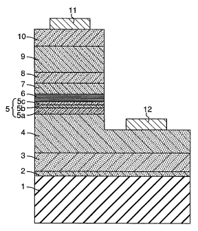
Fig. 1 is a schematic sectional view of an LED device
according to an embodiment of the present invention showing
its layer structure;
CA 02368723 2001-09-26
WO 00/59046 PCT/JPOO/01845
16
Fig. 2 is a schematic graph of a distribution of a p-
type impurity concentration within a low-doped layer of the
present invention, a medium-doped p-cladding layer, and a
high doped p-contact layer; and
Fig. 3 is a graph of an average electrostatic
withstanding voltage against the impurity concentration of
the low-doped layer (average voltage for 100 samples).
Best Mode for Carrying out the Invention
(Embodiment 1)
Fig. 1 is a schematic sectional view of an LED device
according to an embodiment of the present invention.
The nitride semiconductor device according to
Embodiment 1 of the present invention relates to the First
nitride semiconductor device of the present invention, and
the structure of the First nitride semiconductor device is
not limited to the embodiments as described hereinafter.
Rather, the present invention can be applied to any nitride
semiconductor devices which comprises, at least, a medium-
doped p-cladding layer (formed of a p-type multi-film layer
or a p-type single-layered layer), a p-type low-doped layer
doped with a low p-type impurity concentration, and a high-
doped p-contact layer doped with a high p-type impurity
concentration, in which those layers are successively grown
on the active layer.
CA 02368723 2001-09-26
WO 00/59046 PCT/JPOO/01845
17
As shown in Fig. 1, the nitride semiconductor
device of Embodiment 1 comprises a substrate 1, a buffer
layer 2, undoped GaN layer 3, an n-contact layer 4 doped
with n-type impurity, a first n-region multi-film layer 5
which has an undoped lower-film 5a, middle-film 5b doped
with n-type impurity, and an undoped upper-film 5c, a
second multi-film layer 6 having a third and a fourth
nitride semiconductor film, an active layer 7 of the
multiple quantum well structure, a p-cladding layer 8 made
of a p-type multi-film layer or a p-type single-layered
layer, a low-doped p-type layer 9 doped with a low
concentration of p-type impurity, and a high doped p-
contact layer 10 doped with a high concentration of p-type
impurity, in which those layers are formed in this order
the substrate.
The nitride semiconductor device further
comprises an n-electrode 12 formed on the n-contact layer 4,
and p-electrode 11 deposited on the p-contact layer 10.
Details of each layer of the nitride
semiconductor device according to Embodiment 1 will be
described hereinafter.
According to the present invention, the substrate
1 may be made of insulative material such as sapphire
having its principal surface represented by a C-, R- or A-
face or spinel (MgAlz04), or semiconductor material of SiC
CA 02368723 2001-09-26
WO 00/59046 PCT/JPOO/01845
18
(including 6H, 4H or 3C), Si, ZnO, GaAs, GaN, or the like.
Also, the buffer layer 2 may be made of the
nitride semiconductor expressed in a formula of GadAll_dN
(where 0 < d:~ 1) . However, since the buffer layer has
better crystallinity as the composition ratio of Al is less,
the buffer layer 2 preferably has small composition ratio
of Al, and more preferably is made of GaN.
The buffer layer 2 may have a thickness adjusted
to fall within the range of 0.002 through 0.5um, preferably
within the range of 0.005 through 0.2 pm, and more
preferably within the range of 0.01 through 0.02 um, so
that the nitride semiconductor of the buffer layer 2 has
good crystalline morphology, thereby improving the
crystallinity of the nitride semiconductor layers to be
grown on the buffer layer 2.
The growth temperature of the buffer layer 2 is
adjusted to fall within the range of 200 through 900 C and
preferably within the range of 400 through 800 C, so that
the resultant buffer layer 2 exhibits an excellent
polycrystallinity. The buffer layer 2, in turn, act as a
seed crystal to improve the crystallinity of the nitride
semiconductor layers to be grown on the buffer layer 2.
The buffer layer 2 which is grown at a relatively
low temperature may not be essential and may therefore be
eliminated depending on the type of material for the
CA 02368723 2001-09-26
WO 00/59046 PCT/JPOO/01845
19
substrate 1 and/or the growing method employed.
Next, the undoped GaN layer 3 is formed on the
buffer layer 2 by depositing GaN on the buffer layer 2 and
doping no n-type impurity into the GaN layer. The undoped
GaN layer 3 grown on the buffer layer 2 can be formed with
a good crystallinity, which in turn, allows the n-contact
layer 4 subsequently deposited on the undoped GaN layer 3
to have a good crystallinity. The undoped GaN layer 3 has
a thickness not thinner than 0.01um, preferably not thinner
than 0.5}.im, and more preferably not thinner than 1um. If
the undoped GaN layer 3 has a thickness as specified above,
the other layers to be successively grown over the undoped
GaN layer 3 have good crystallinity. Although the upper
limit of thickness of the undoped GaN layer 3 may not be
essential for the invention and therefore not specified, it
should be properly adjusted in consideration of the
manufacturing efficiency. Also, the uppermost thickness of
the undoped GaN layer 3 may be preferably adjusted so that
the total thickness of the undoped GaN layer 3, the n-
contact layer 4, and the first n-region multi-film layer 5
falls within the range of 3 through 20}.im (preferably within
the range of 3 through 10um, more preferably within the
range of 4 through 9pm) in order to improve the
characteristics of the electrostatic withstanding voltage.
According to the present invention, the n-contact
CA 02368723 2001-09-26
WO 00/59046 PCT/JPOO/01845
layer 4 doped with n-type impurity contains the n-type
impurity in the concentration of not less than 3 x 10¹⁸/cm3,
and preferably not less than 5 x l018/cm3. The use of the
relatively high concentration of the n-type impurity in the
5 n-contact layer 4 is effective to lower the Vf (forward
voltage) and threshold current. On the other hand, if the
concentration of the n-type impurity departs from the range
specified above, the Vf will hardly lower. Since the n-
contact layer 4 is formed on the undoped GaN layer 3 having
10 low concentration of n-type impurity and a good
crystallinity, the n-contact layer has a good crystallinity
even though it contains the relatively high concentration
of the n-type impurity. Although the present invention
does not specifically require the uppermost concentration
15 limit of the n-type impurity concentration within the n-
contact layer 4, the uppermost limit is preferably not
greater than 5 x 10²¹/cm', which allows the contact layer 4
capable of functioning as a contact layer.
The n-contact layer 4 may be formed of material
20 expressed as the general formula of IneAlfGal_e_fN (where 0<-
e, 0<- f, and e+f <- 1) . However, the use of GaN or A1fGa1_
fN where suffix f is not greater than 0.2 is advantageous
in that the nitride semiconductor layer having a minimized
crystal defect can easily be obtained. The n-contact layer
4 may, although not limited thereto, have a thickness
CA 02368723 2001-09-26
WO 00/59046 PCT/JP00/01845
21
within the range of 0.1 through 20um, preferably within the
range of 1.0 through 10um, so that the n-contact layer 4 on
which the n-electrode 12 is formed can be formed with a low
resistivity thereby to reduce the Vf.
Also, the uppermost thickness of the n-contact
layer 4 can be preferably adjusted so that the total
thickness of the undoped GaN layer 3, the n-contact layer 4,
and the first n-region multi-film layer 5 falls within the
range of 3 through 20um (preferably within the range of 3
through 20um, more preferably within the range of 4 through
9pm), which allows the electrostatic withstanding voltage
to be improved.
And the n-contact layer 4 can be omitted by
forming the first n-region multi-film layer 5 relatively
thick.
Next, according to Embodiment 1, the first n-
region multi-film layer 5 includes three films of an
undoped lower-film 5a, a middle-film 5b doped with n-type
impurity and an undoped upper-film 5c. It is noted that
any other films may be included in the first multi-film
layer 5 according to the present invention. Also, the
first n-region multi-film layer 5 may contact with the
active layer, alternatively, an another layer may be
interposed between the active layer and the first n-region
multi-film layer. In case where the first n-region multi-
CA 02368723 2001-09-26
WO 00/59046 PCT/JPOO/01845
22
film layer is formed in the n-region as Embodiment 1, the
device characteristics such as the luminous intensity and
the electrostatic withstanding voltage can be improved.
Therefore, it is understood that the first n-region multi-
film layer 5 substantially contributes the improved
electrostatic withstanding voltage.
The nitride semiconductor including the lower-
film 5a through the upper-film 5c can be formed of various
composition of the nitride semiconductor expressed in a
formula of IngAlr,Gal_9_,,N (0 <_ g < 1, 0<_ h< 1), and
preferably, it is made of the composition of GaN. Also the
composition of each film of the first n-region multi-film
layer 5 may be same or different.
Although the thickness of the first n-region
multi-film layer 5 may fall within the range of 175 through
12000 angstroms, preferably within the range of 1000
through 10000 angstroms, more preferably in the range of
2000 through 6000 angstroms.
Also, the thickness of the first n-region multi-
film layer 5 is preferably adjusted with the aforementioned
range, and in addition to that, the total thickness of the
undoped GaN layer 3, the n-contact layer 4, and the first
n-region multi-film layer 5 falls within the range of 3
through 20um (preferably within the range of 3 through 101im,
more preferably within the range of 4 through 9um), which
CA 02368723 2001-09-26
WO 00/59046 PCT/JPOO/01845
23
allows the electrostatic withstanding voltage to be
improved.
The total thickness of the first n-region multi-
film layer 5 may be adjusted to fall within the above-
mentioned range by adjusting each thickness of the lower-
film 5a, the middle-film 5b, and the upper-film 5c.
Although each thickness of the lower-film 5a, the
middle-film 5b, and the upper-film 5c, which composes the
first n-region multi-film layer 5, are not specifically
limited thereto according to the present invention, each
thickness of the films of the first n-region multi-film
layer 5 has slightly different impact to the device
characteristics. Therefore, in order to optimize the
device characteristics, in consideration of the device
characteristics most influenced by each thickness of the
three films, the preferable ranges for each film thickness
can be determined by fixing two films and gradually varying
the thickness of the other film.
Even though each film alone of the first n-region
multi-film layer 5 may not influence the electrostatic
withstanding voltage, the combination of the films of the
first n-region multi-film layer 5 may improve the various
device characteristics as a whole. In particular, the
first n-region multi-film layer 5 combined with such films
can greatly improve the luminous intensity and the
CA 02368723 2001-09-26
WO 00/59046 PCT/JPOO/01845
24
electrostatic withstanding voltage of the device. Such
effect can be approved after the device including the first
n-region multi-film layer 5 is actually produced. Showing
some particular thickness of each film, the tendency of
change of the device characteristics influenced by the
various thickness of each film will be described
hereinafter.
The thickness of the lower-film 5a falls within
the range of 100 through 10000 angstroms, preferably within
the range of 500 through 8000 angstroms, and more
preferably within the range of 1000 through 5000 angstroms.
As the lower-film 5a gradually becomes thicker, the
electrostatic withstanding voltage becomes higher, while
the Vf increases rapidly around at 10000 angstroms. On the
other hand, as the lower-film 5a becomes thinner, the Vf
decreases while the electrostatic withstanding voltage
decreases so that the productivity tends to be reduced at
the thickness less than 100 angstroms due to the lower
electrostatic withstanding voltage. Since the lower-film
5a is provided to improve the crystallinity which are
deteriorated by the contact layer 4 doped with n-type
impurity, the lower-film 5a is preferably grown with a
thickness of 500 through 8000 angstroms in order to
efficiently improve the crystallinity of the layers to be
formed subsequently on the lower-film.
CA 02368723 2001-09-26
WO 00/59046 PCT/JPOO/01845
The thickness of the middle-film 5b doped with n-
type impurity falls within the range of 50 through 1000
angstroms, preferably within the range of 100 through 500
angstroms, and more preferably within the range of 150
5 through 400 angstroms. The middle-film 5b doped with n-
type impurity has a carrier concentration sufficiently high
to intensify the luminous intensity. The light emitting
device without the middle-film 5b has luminous intensity
less than that having this film. Contrary to this, where
10 the thickness of the middle-film Sb is over than 1000
angstroms, the luminous intensity is reduced. Meanwhile,
the electrostatic withstanding voltage is improved as the
middle-film 5b is thicker, but it is reduced as the
thickness is less than 50 angstroms in comparison with that
15 where the thickness is over 50 angstroms.
The thickness of the undoped upper-film 5c falls
within the range of 25 through 1000 angstroms, preferably
within the range of 25 through 500 angstroms, and more
preferably within the range of 25 through 150 angstroms.
20 The undoped upper-film Sc among the first n-region multi-
film layer is formed in contact with, or most adjacent to
the active layer 6 preventing the current from leaking.
Where the thickness of the upper-film Sc is less than 25
angstroms, it can not efficiently prevent the current from
25 leaking. And where the thickness of the upper-film 5c is
CA 02368723 2001-09-26
WO 00/59046 PCT/JP00/01845
26
over 1000 angstroms, then the Vf is increased and the
electrostatic withstanding voltage is reduced.
As described above, considering the device
characteristics particularly influenced by either one of
the lower-film 5a through the upper-film 5c, the thickness
of each film, which are combined to form the first n-region
multi-film layer 5, is adjusted so that every device
characteristics is equally optimized, in particular, the
luminous intensity and the electrostatic withstanding
voltage are optimized. Also, the thickness of each of the
lower-film 5a, the middle-film 5b, and the upper-film 5c is
adjusted to fall within the aforementioned range, and the
aforementioned three p-type layers with different p-type
impurity concentration according to the present invention
are appropriately combined with the first n-region multi-
film layer 5 so that the luminous intensity, the product
reliability, as well as the electrostatic withstanding
voltage of the device products can be improved.
In other words, each thickness of the films of
the first n-region multi-film layer 5 are determined so
that the device characteristics is optimized in
consideration of the relation between the p-type three
layers of the present invention and the first n-region
multi-film layer 5, the composition of the active layer
varying corresponding to the wavelength, the condition
CA 02368723 2001-09-26
WO 00/59046 PCT/JPOO/01845
27
required by the device specification such as dimensions and
configurations depending on the LED device and the like.
Each film of the first multi-film layer 5 is made
of composition, which may be expressed in the formula of
IngAlhGal_g_,,N (0 <- g < 1, 0- h < 1) and may be same or
different from those of the other films. However,
according to the present invention, the films of the first
multi-film layer 5 have the composition ratios of In and Al
are small, and preferably are made of Al,,Gal_hN in order to
improve the crystallinity thereof and reduce the Vf, and
more preferably of GaN. Where the first n-region multi-
film layer 5 is made of Al,,Gal_,,N, the composition ratio of
Al can be adjusted to fall within the range of 0<- h < 1,
as mentioned above, as the composition ratio of Al is
smaller, then the crystallinity can be improved and the Vf
is reduced.
The middle-film 5b has the n-impurity
concentration not less than 3 x 10¹⁸/cm3, and preferably not
less than 5 x 10¹⁸/cm3. The upper limit of the n-impurity
concentration thereof is preferably not greater than 5 x
1021/cm3, where the middle-film 5b has the n-impurity
concentration within the range, the films can be grown with
a comparatively good crystallinity, thereby reducing the Vf
while maintaining the high luminous intensity.
An n-type impurity element may be selected from
CA 02368723 2001-09-26
WO 00/59046 PCT/JPOO/01845
28
IVB or VIB Groups in the periodic table such as Si, Ge, Se,
S, and 0, preferably Si, Ge, or S is used for the n-type
impurity.
In case where the active layer 6 is formed on the
first n-region multi-film layer 5, the upper-film 5c of the
first n-region multi-film layer 5 which is formed in
contact with the active layer 6 may act as a barrier layer
by forming the upper-film 5c of GaN.
In other words, the lower-film 5a and upper-film
5c among the first n-region multi-film layer 5, which
actually contact with an another layer may be formed as a
part having an another function in connection with the
other layer.
Also, according to the present invention, an
undoped single-layered layer may be used instead of the
first n-region multi-film layer S. Although the single-
layered layer may be made of nitride semiconductor as
expressed in a general formula of In,,Al,,Gal_g_hN (0 <- g < 1,
0<- h < 1) , the composition ratios of In and Al contained
in the undoped single-layered layer are small, and
preferably it is made of Al,,Gal_,,N, and more preferably of
GaN. Where the undoped single-layered layer 5 is made of
Al,,Gal_,,N, the composition ratio of Al can be adjusted to
fall within the range of 0<_ h < 1. Preferably the
composition ratio of the Al should be small, since the
CA 02368723 2001-09-26
WO 00/59046 PCT/JP00/01845
29
crystallinity can be improved and the Vf is reduced as the
composition ratio of Al is smaller. In case where the
undoped singled-layered layer is grown, the electrostatic
withstanding voltage is not as good as that in case where
the first n-region multi-film layer 5 is grown, but is
better than that of the conventional devices. Other device
characteristics are almost as good as those in case where
the first n-region multi-film layer 5 is grown.
Although the thickness of the single-layered
layer is not specifically limited, preferably falls within
the range of 1000 through 3000 angstroms.
Next, according to the present invention, a
second n-region multi-film layer 6 is composed of a third
nitride semiconductor film and a fourth nitride
semiconductor film having different composition from that
of the third nitride semiconductor film. At least one of
each of the third and fourth nitride semiconductor films is
laminated alternatively (at least two films in total).
Preferably three films and more preferably at least two
films (at least four films) in total are laminated
alternately.
At least one of the third and the fourth films of
the second n-region multi-film layer 6 is set to have a
thickness of 100 angstroms or less, preferably 70 angstroms
or less, more preferably 50 angstroms or less. Further
CA 02368723 2001-09-26
WO 00/59046 PCT/JPOO/01845
more preferably, both of the third and the fourth film of
the second n-region multi-film layer 6 are set to have
thickness of 100 angstroms or less, preferably 70 angstroms
or less, more preferably 50 angstroms or less. The second
5 n-region multi-film layer 6 is formed with such thin films
to be of a superlattice structure so that the crystallinity
of the second n-region multi-film layer 6 is enhanced
thereby improving the luminous intensity.
At least one of the third and fourth films has
10 thickness of 100 angstroms or less, which is thinner than
the critical elastic thickness so that the crystallinity is
improved. Where the crystallinity of such thin film is
improved, then the another film formed on the thin film can
be also formed with the improved crystiallinity, so that
15 the second n-region multi-film layer as a whole has a good
crystallinity thereby improving the luminous intensity.
Also, both of the third and fourth films have
thickness of 100 angstroms or less, which are thinner than
the critical elastic thickness so that the crystallinity of
20 the nitride semiconductor films are more improved in
comparison with the case where it is formed of a single-
layered layer or where either one of the third and fourth
film has the critical elastic thickness. Where the
thickness of both of the third and fourth nitride
25 semiconductor films are 70 angstroms or less, the second n-
CA 02368723 2001-09-26
WO 00/59046 PCT/JPOO/01845
31
region multi-film layer 6 is formed of superlattice
structure, so that much more improved crystallinity can be
achieved. The active layer 7 formed on the second n-region
multi-film layer 6 can be formed with a greatly improved
crystallinity as the second n-region multi-film layer 6
acts as a buffer layer.
As described above, the three layers having
different p-type impurity concentration according to the
present invention are combined with the first and second n-
region multi-film layer so that the light emitting device
can be obtained with very high luminous intensity and low
Vf. The reason is not clearly explained but presumably,
the crystallinity of the active layer formed on the second
n-region multi-film layer is improved.
Adjacent two of the third nitride semiconductor
films sandwiching the fourth nitride semiconductor film
among the second n-region multi-film layer 6 have thickness
that are same or different each other.
Adjacent two of the fourth nitride semiconductor
films sandwiching the third nitride semiconductor film
among the second n-region multi-film layer 6 have thickness
that are same or different each other.
In particular, where the third and fourth nitride
semiconductor film are made of the InGaN and GaN,
respectively, the thickness of each of the third nitride
CA 02368723 2001-09-26
WO 00/59046 PCT/JPOO/01845
32
semiconductor films of InGaN can be thicker or thinner as
the third nitride semiconductor film is closer to the
active layer, so that the refractive index of the second n-
region multi-film layer can be substantially and gradually
varied. Therefore, the resultant nitride semiconductor
layer achieves the same effect as it has the substantially
gradient composition. In such formed device that requires
beam waveguides like a laser device, the beam waveguides
are formed with the multi-film layer so that the mode of
the laser beam can be adjusted.
Also, adjacent two of the third nitride
semiconductor films sandwiching the fourth nitride
semiconductor film of the second n-region multi-film layer
6 have a composition that are same or different each other.
In addition, adjacent two of the fourth nitride
semiconductor films sandwiching the third nitride
semiconductor film of the second n-region multi-film layer
6 have a composition ratio of the III group element that
are same or different each other.
In particular, where the third and fourth nitride
semiconductor film are made of the InGaN and GaN,
respectively, the In composition ratio of each of the third
nitride semiconductor films of InGaN may be gradually
increased or decreased as the third nitride semiconductor
film is closer to the active layer, so that such formed
CA 02368723 2001-09-26
WO 00/59046 PCT/JPOO/01845
33
second n-region multi-film layer of nitride semiconductor
has substantially gradient composition and the refractive
index thereof can be varied. It is noted that as the In
composition ratio is decreased, the refractive index is
reduced.
The second n-region multi-film layer 6 may be
formed spaced away from the active layer, preferably in
contact with the active layer. The second n-region multi-
film layer 6 formed in contact with the active layer
contributes more luminous intensity.
Where the second n-region multi-film layer 6 is
formed in contact with the active layer, the first film
thereof contacting with the firstly laminated layer (well
layer or barrier layer) of the active layer may be the
third nitride semiconductor film or the fourth nitride
semiconductor film, and the laminating order of the third
and fourth nitride semiconductor films are not specifically
limited thereto. Although Fig. 1 shows the second n-region
multi-film layer 6 formed in contact with the active layer
7, an another n-type nitride semiconductor layer may be
interposed between the active layer 7 and the second n-
region multi-film layer 6.
The third nitride semiconductor film is made of a
nitride semiconductor containing In, or preferably a
ternary compound of InkGal_kN (0 < k < 1) , is characterized
CA 02368723 2001-09-26
WO 00/59046 PCT/JPOO/01845
34
in that suffix k is preferably not greater than 0.5 and
more preferably not greater than 0.2. On the other hand,
the fourth nitride semiconductor film may be made of any
suitable nitride semiconductor, which is different from
that of the third nitride semiconductor film. Although not
specifically limited thereto, the fourth nitride
semiconductor film may be made of binary or ternary
compound expressed ion the formula of InõGal_n,N (0 - m < 1,
and m < k), which has bandgap higher than that of the third
nitride semiconductor film to have an excellent
crystallinity. Preferably, the fourth nitride
semiconductor film may be made of GaN to have a good
crystallinity. Therefore, the third and fourth nitride
semiconductor films are preferably made of InkGal_kN (0 < k
< 1) and In,,Gal-n,N (0 <_ m < 1, and m < k) (GaN is more
preferable), respectively. More preferably, the third and
fourth nitride semiconductor films are made of InkGal_kN (k
<- 0.5) and GaN, respectively.
Both of, either one of, or none of the third and
fourth nitride semiconductor films may be doped with n-type
impurity. In order to improve the crystallinity thereof,
the films may be preferably modulation-doped, and more
preferably, both of them are undoped. It is noted that
where both of the third and fourth nitride semiconductor
films are doped, the impurity concentration thereof may be
CA 02368723 2001-09-26
WO 00/59046 PCT/JPOO/01845
different from each other.
Also it is noted that the layer, in which either
one of the third and fourth nitride semiconductor film is
doped with n-type impurity, is referred to as a modulation-
5 doped layer, such modulation-doped layer contributes the
higher luminous intensity.
An element selected from IV or VI Group in the
periodic table such as Si, Ge, Sn, and S is used as the n-
type impurity, preferably Si or Sn is used for the n-type
10 impurity. The impurity concentration is adjusted to be not
greater than 5 x 10²¹/cm3 and preferably not greater than 1
x 1020/cm3. If the impurity concentration is greater than 5
x 1021/cm3, the crystallinity of the nitride semiconductor
films will be deteriorated, thereby reducing the luminous
15 intensity. This is also applied for the case where the
layer is modulation-doped.
According to the present invention, the active
layer 7 of the multiple quantum well structure is formed of
nitride semiconductor containing In and Ga, preferably
20 InaGa,_aN (where 0_ a < 1) . Further, although the active
layer 7 may be doped with n-type or p-type impurity,
preferably is undoped (with no impurity added), so that a
strong band-to-band light emission can be obtained with the
half width of the emission wavelength narrowed. The active
25 layer 7 may be doped with either n-type impurity or p-type
CA 02368723 2001-09-26
WO 00/59046 PCT/JPOO/01845
36
impurity or even with both impurity. Where the active
layer 7 is doped with n-type impurity, the band-to-band
light emission strength can further be increased as
compared with the undoped active layer 7. On the other
hand, the active layer 7 is doped with p-type impurity, so
that the peak wavelength is shifted towards that having
energy level less by 0.5 eV and the spectrum has the half
width widened. The active layer doped with both of n-type
and p-type impurity has the luminous intensity greater than
that emitted by the active layer doped only with the p-typ.e
impurity. In particular, where the active layer doped with
a p-type dopant is formed, the active layer preferably has
an n-type conductivity as a whole by doping an n-type
dopant such as Si therein. In order to grow the active
layer with a good crystallinity, the active layer is
preferably doped with no impurity, that is, non-doped.
Also, according to Embodiment 1, the device
having the active layer formed of single quantum well
structure has the electrostatic withstanding voltage as
good as that of the multiple quantum well structure,
although the former has luminous intensity less than that
of the later.
The sequence of lamination of barrier and well
layers forming the active layer 7 may start with the well
layer and terminate with the well layer, or start with the
CA 02368723 2001-09-26
WO 00/59046 PCT/JPOO/01845
37
well layer and terminate with the barrier layer.
Alternatively, the sequence may start with the barrier
layer and terminate with the barrier layer or start with
the barrier layer and terminate with the well layer. The
well layer has thickness adjusted to be not greater than
100 angstroms, preferably not greater than 70 angstroms and
more preferably not greater than 50 angstroms. Although
not specifically limited, the lowermost limit of thickness
of the well layer may correspond to thickness of a single
atom layer and, preferably not smaller than 10 angstroms.
If the well layer is greater than 100 angstroms, the
luminous intensity will be difficult to increase.
On the other hand, the barrier layer has
thickness adjusted to be not greater than 2,000 angstroms,
preferably not greater than 500 angstroms and more
preferably not greater than 300 angstroms. Although not
specifically limited, the lowermost limit of thickness of
the barrier layer may correspond to the film thickness of a
single atom layer and, preferably not smaller than 10
angstroms. If the thickness of the barrier layer falls
within the above-specified range, the luminous intensity
can be increased advantageously. In addition, the
thickness of the active layer 7 in total is not
specifically limited to a particular value, but the active
layer 7 may have a total film thickness by adjusting the
CA 02368723 2001-09-26
WO 00/59046 PCT/JP00/01845
38
number of the barrier and well layers laminated and/or the
sequence of lamination thereof in consideration of the
desired wavelength of the eventually resulting LED device.
According to the present invention, the p-
cladding layer 8 is formed as a multi-film layer or a
single-layered layer with p-type impurity such that the
concentration thereof may contain a medium concentration
(medium-doped) between those of the p-type low-doped layer
9 and the high-doped p-contact layer 10.
Where the p-cladding layer 8 made of he multi-
film layer (superlattice structure) will be described
hereinafter. A p-cladding layer made of a multi-film layer
is referred hereinafter as a multi-film p-cladding layer.
Films composing the multi-film p-cladding layer
are a first nitride semiconductor film containing Al and a
second nitride semiconductor film with different
composition from that of the first nitride semiconductor
film. At least ones of first and second nitride
semiconductor films include the p-type impurity. The case
where the first and second nitride semiconductor film has
different composition each other will be rephrased
hereinafter as that they have different bandgap each other.
According to the present invention, the multi-
film p-cladding layer 8 may be formed by alternately
laminating the first nitride semiconductor film and the
CA 02368723 2001-09-26
WO 00/59046 PCT/JPOO/01845
39
second nitride semiconductor film with bandgap greater than
that of the first nitride semiconductor film. At least one
of the first and second nitride semiconductor films
contains p-type impurity, and the p-type impurity
concentration may be same or different.
The first and second nitride semiconductor films
have thickness adjusted to be 100 angstroms or less,
preferably 70 angstroms or less, and more preferably in the
range of 10 through 40 angstroms. And the thickness of
both films may be same or different. Each film has the
thickness within the above-mentioned range so that each
thickness is thinner than the critical elastic thickness,
thereby having a good crystallinity in comparison with the
thick layer of the nitride semiconductor layer. Thus, a p-
layer doped with p-type impurity having the higher carrier
concentration and the reduced resistibility can be grown,
so that the Vf and threshold value can be reduced. The
multi-film layer is grown by laminating a plurality of the
two types (as a pair) of films having thickness specified
above of films. Either ones of the first and second
nitride semiconductor films are deposited more by one time
than the others. In particular, the first nitride
semiconductor film is firstly and also lastly laminated.
And the total thickness of the multi-film p-cladding layer
8 may be set by adjusting the thickness and laminating
CA 02368723 2001-09-26
WO 00/59046 PCT/JPOO/01845
numbers of the first and second nitride semiconductor films.
Although the total thickness of the multi-film p-cladding
layer 8 is, not specifically limited thereto, 2000
angstroms or less, preferably 1000 angstroms or less, and
5 more preferably 500 angstroms or less. The total thickness
of the layer falls within the above-mentioned range, so
that its luminous intensity can be increased and the Vf can
be decreased.
The first nitride semiconductor film is formed of
10 nitride semiconductor containing at least Al preferably
expressed in the formula of Al,,Gal_õN (where 0 < n<- 1).
Meanwhile, the second nitride semiconductor film is formed
of binary or ternary compound nitride semiconductor such as
AlPGaI_pN (where 0<_ p < 1 and n > p) or InrGal_rN (where 0<-
15 r- 1). Where the p-cladding layer 8 is grown of the
multi-film layer laminating alternately the first and
second nitride semiconductor film, the Al composition ratio
of the p-type multi-film layer will be referred to as an
average ratio across the layer. Also, where the p-type
20 low-doped layer 9 as described hereinafter is formed of
AlsGal_sN (where 0 < s < 0.5) or is grown with multi-film
structure including films of Al Gal_sN (where 0 < s < 0. 5) ,
the Al composition ratio of the multi-film p-cladding layer
is preferably adjusted to be greater than that of the p-
25 type low-doped layer 9, so that the luminous intensity and
CA 02368723 2001-09-26
WO 00/59046
PCT/JP00/01845
41
the electrostatic withstanding voltage can be
advantageously improved.
Further the p-cladding layer 8 is formed of the
superlattice structure so that the device has the improved
crystallinity, the reduced resistibility, and the reduced
Vf.
The p-type impurity concentration of the medium-
doped p-cladding layer 8 will be described hereinafter.
The p-type impurity concentration of the first
and second nitride semiconductor film may be same or
different each other.
Firstly, the case where the p-type impurity
concentration of the first and second nitride semiconductor
film is different each other will be described hereinafter.
Where the p-type impurity concentration of the
first and second nitride semiconductor film is different
each other, for example, the p-type impurity concentration
of the first nitride semiconductor film with bandgap
greater than that of the second nitride semiconductor film
may be adjusted greater than that of the second nitride
semiconductor film.
Alternately, the p-type impurity concentration of
the first nitride semiconductor film with bandgap greater
than that of the second nitride semiconductor film may be
adjusted less than that of the second nitride semiconductor
CA 02368723 2001-09-26
WO 00/59046 PCT/JPOO/01845
42
film.
As described above, the formation of the first
and second nitride semiconductor film having different the
p-type impurity concentration can reduce the threshold
voltage, the Vf, or the like.
This is because the formation of the first
nitride semiconductor film with high impurity concentration
that leads high carrier density and second nitride
semiconductor film with low impurity concentration that
leads high carrier mobility in the multi-film p-cladding
layer 8 may cause a great number of carrier from the film
with high carrier density move in the film with high
carrier mobility, so that the resistibility of the multi-
film layer can be reduced. Thus, the device has the
threshold voltage the Vf reduced as mentioned above.
It is noted that where the first and second
nitride semiconductor films are formed with p-type impurity
concentration different from each other, the film having
lower p-type impurity concentration is preferably undoped,
so that the threshfold voltage, the Vf (the forward
voltage), or the like can be further reduced.
Where the first and second nitride semiconductor
films have p-type impurity concentration different from
each other, the p-type impurity concentration of the first
nitride semiconductor film is adjusted such that the
CA 02368723 2001-09-26
WO 00/59046 PCT/JPOO/01845
43
average p-impurity concentration of the multi-film layer is
greater than that of the low-doped layer 9 and less than
that of the p-contact layer 10. In particular, the p-type
impurity concentration of the first nitride semiconductor
film is adjusted to fall within the range of 5 x 10¹⁷/cm3
through 1 x 10²¹/cm3, preferably 5 x 10¹⁸/cm3 through 5 x
1020/cm3.
Where the p-type impurity concentration of the
first nitride semiconductor film is greater than 5 x
101'/cm3, the injection efficiency into the active layer 7
is improved resulting in the higher luminous intensity and
the lower Vf. Also, where the p-type impurity
concentration of the first nitride semiconductor film is
less than 1 x 10²¹/cm3, the crystallinity shows the tendency
to be good.
Where the first and second nitride semiconductor
films have p-type impurity concentration different from
each other, the p-type impurity concentration of the second
nitride semiconductor film is adjusted such that the
average p-impurity concentration of the multi-film layer is
greater than that of the low-doped layer 9 and less than
that of the p-contact layer 10. In particular, although
not specifically thereto, the second nitride semiconductor
film has the p-type impurity concentration which is less
than one-tenth of the p-type impurity concentration of the
CA 02368723 2001-09-26
WO 00/59046 PCT/JPOO/01845
44
first nitride semiconductor film, or preferably is undoped.
Nevertheless, the second nitride semiconductor film has the
thickness that is so thin that some of the p-type impurity
within the first nitride semiconductor film is diffused
into the second nitride semiconductor film. In
consideration of the mobility of the second nitride
semiconductor film is preferably not greater than 1 x
1020/cm3.
Also, this is also applied for the case where the
p-type impurity concentration of the first nitride
semiconductor film with bandgap greater than that of the
second nitride semiconductor film may be adjusted less than
that of the second nitride semiconductor film.
Next, in case where both of the first and second
nitride semiconductor films have the same p-type impurity
concentration, the p-type impurity concentration will be
described hereinafter.
In this case, the p-type impurity concentration
of the first and second nitride semiconductor films may be
adjusted to be more than that of the p-type low-doped layer
9 and less than that of the p-contact layer 10. In
particular, the range of the p-type impurity concentration
of the first and second nitride semiconductor films is
similar to that of the first nitride semiconductor film in
case where the first and second nitride semiconductor films
CA 02368723 2001-09-26
WO 00/59046 PCT/JP00/01845
have different p-type impurity concentration. Where the
first and second nitride semiconductor films have the same
p-type impurity concentration, then the p-cladding layer 8
has the crystallinity less than that in case where they
5 have different p-type impurity concentration. However, the
p-cladding layer 8 can be easily grown with high carrier
density to have the increased luminous intensity,
advantageously.
The p-type impurity doped into the aforementioned
10 p-cladding layer is selected from elements of the IIA or
IIB Group, such as Mg, Zn Ca, and Be, preferably is Mg, Ca,
or the like.
In case where the aforementioned medium-doped
multi-film p-cladding layer 8 is formed by alternately
15 laminating a plurality of the first and second nitride
semiconductor films that have different p-type impurity
concentration, ones of the higher doped nitride
semiconductor films are laminated with p-type impurity
concentration, which are gradually less (preferably
20 undoped) towards end portions of the p-cladding layer 8
along the thickness direction thereof, and are higher
around the middle of the p-cladding layer 8. Thus, the
resistibility thereof can be advantageously reduced.
Next, the case where the single-layered p-
25 cladding layer is made of AlbGal_bN (0 <_ b<- 1) containing
CA 02368723 2001-09-26
WO 00/59046 PCT/JPOO/01845
46
the p-type impurity will be described hereinafter. The p-
cladding layer 8 formed of a single layer is referred to as
a single-layered p-cladding layer.
According to the present invention, the single-
layered p-cladding layer 8 is formed of nitride
semiconductor of AlbGal_bN (0 - b<- 1) as described. And in
case where the p-type low-doped layer 9 as will be
discussed later is formed of AlsGal_ N(0 < s < 0.5) , the Al
composition ratio of the single-layered p-cladding layer 8
is adjusted greater than that of the p-type low-doped layer
9, so that the higher luminous intensity as well as greater
electrostatic withstanding voltage can be advantageously
achieved. Also, the single-layered p-cladding layer 8
containing no Al has the luminous intensity less than that
containing Al, but has the electrostatic withstanding
voltage as high as that containing Al.
Although not specifically limited thereto, in
order to improve the luminous intensity and to reduce the
Vf, the thickness of the single-layered p-cladding layer 8
is 2000 angstroms or less, preferably 1000 angstroms or
less, more preferably in the range of 500 through 100
angstroms.
The p-type impurity concentration of the single-
layered p-cladding layer 8 is adjusted to fall within the
range of 5 x 10¹⁷/cm3 through 1 x 10²¹/cm3, preferably in the
CA 02368723 2001-09-26
WO 00/59046 PCT/JP00/01845
47
range of 5 x 10¹⁸/cm3 through 5 x 10²⁰/cm3, so that the
single-layered with an improved crystallinity, thereby
increasing the luminous intensity, advantageously.
Although the single-layered p-cladding layer 8
has crystallinity less than but almost as good as the
multi-film p-cladding layer, the manufacturing steps of the
p-cladding layer 8 can be simplified because of the single-
layered layer.
Next, according to the present invention, the p-
type low-doped layer 9 that is doped with low impurity
concentration can be formed of various nitride
semiconductor expressed in the general formula of InrAlsGal_
r_SN (0 <- r < 1, 0<- s< 1, r + s < 1), preferably formed of
the ternary compound nitride semiconductor such as InrGal_rN
(0 <- r < 1) or A1sGa1_SN (0 <- s < 1) , more preferably formed
of the binary nitride compound semiconductor of GaN because
of the crystallinity. Thus, the p-type low-doped layer 9
is formed of GaN to have the crystallinity improved and the
electrostatic withstanding voltage increased. Where the p-
type low-doped layer 9 is made of the ternary nitride
compound semiconductor as expressed in the formula of
A1sGa1_sN (0 <- s < 1) , the Al composition ratio (or an
average Al composition ratio where the layer 9 is made of
multi-film layer) of the ternary nitride compound
semiconductor is adjusted to be less than the average Al
CA 02368723 2001-09-26
WO 00/59046 PCT/JPOO/01845
48
composition ratio of the aforementioned multi-film p-
cladding layer 8 or the single-layered p-cladding layer 8,
so that the low-doped layer 9 of ternary nitride compound
semiconductor causes the forward voltage (Vf) suppressed,
and also the luminous intensity and electrostatic
withstanding voltage improved as good as the that made of
GaN.
Also, in case where the p-type low-doped layer 9
is made of nitride semiconductor of Al5Ga1_sN (0 < s < 0.5),
and the Al composition ratio of the p-type low-doped layer
9 is less than that of the p-cladding layer 8, the p-type
low-doped layer 9 can be formed with high luminous
intensity and the electrostatic withstanding voltage even
when the p-type low-doped layer 9 is thinner than that in
case where being made of GaN. Therefore, the growth time
can be shortened in comparison with the GaN p-cladding
layer 8.
According to Embodiment 1 of the invention, the
p-type low-doped layer 9 can be formed as a multi-film
layer by alternately laminating a plurality of two types of
nitride semiconductor films. The similar characteristics
to that of the single-layered layer can be obtained.
Where the p-type low-doped layer 9 can be formed
of a multi-film layer, preferably, ones of nitride
semiconductor films are made of AlsGal_SN (0 < s < 0.5), and
CA 02368723 2001-09-26
WO 00/59046 PCT/JPOO/01845
49
another ones of nitride semiconductor films are made of GaN,
so that the average of Al composition ratio of the p-type
low-doped layer 9 is adjusted less than that of the p-
cladding layer 8.
In case where the p-type low-doped layer 9 is
composed of the multi-film layer having nitride
semiconductor films made of AlsGal_sN (0 < s < 0.5) or
having nitride semiconductor films made of Al5Ga1_sN (0 < s
< 0.5) and nitride semiconductor films made of GaN, then
the crystallinity of the p-type low-doped layer 9 can be
improved and the electrostatic withstanding voltage can be
increased.
Also, where the p-type low-doped layer 9 is
formed of a multi-film layer, in order to improve the
crystallinity thereof, each film has the thickness
preferably in the range of several angstroms through 100
angstroms.
According to the present invention, the p-type
low-doped layer 9 has a thickness within the range of 100
through 10000 angstroms, preferably 500 through 8000
angstroms, and more preferably 1000 through 4000 angstroms,
in order to improve the luminous intensity and the
electrostatic withstanding voltage.
Also, in case where the p-type low-doped layer 9
is made of nitride semiconductor of AlsGal_sN (0 < s < 0.5),
CA 02368723 2001-09-26
WO 00/59046 PCT/JPOO/01845
and the Al composition ratio of the p-type low-doped layer
9 is less than that of the p-cladding layer 8, or in case
where the p-type low-doped layer 9 is made of nitride
semiconductor films of AlsGal_sN (0 < s < 0.5), and the Al
5 composition ratio of the p-type low-doped layer 9 is less
than that of the p-cladding layer 8, the thickness of the
low-doped layer 9 has a thickness within the range of 100
through 10000 angstroms, preferably 300 through 5000
angstroms, and more preferably 300 through 3000 angstroms.
10 Also, in case where the p-type low-doped layer 9 is made of
nitride semiconductor of AlsGai_sN (0 < s < 0.5), and the Al
composition ratio of the p-type low-doped layer 9 is less
than that of the p-cladding layer 8, the p-type low-doped
layer 9 can be formed with a good characteristics even when
15 the p-type low-doped layer 9 is thinner than that in other
cases.
According to the present invention, as described
above, the p-type impurity concentration of the low-doped
layer 9 is adjusted to be less than that of the p-cladding
20 layer 8 and the p-contact layer 10.
Like this, the p-type low-doped layer 9 having
the p-type impurity concentration less than that of the p-
contact layer 10 and greater than that of the p-cladding
layer 8 are grown between the p-contact layer 10 and the p-
25 cladding layer 8, so that the luminous intensity as well as
CA 02368723 2001-09-26
WO 00/59046 PCT/JPOO/01845
51
the electrostatic withstanding voltage can be improved.
Although the p-type impurity concentration of the
low-doped layer 9 is not specifically limited thereto if it
is less than that of the p-cladding layer 8 and the p-
contact layer 10, the p-type impurity concentration of the
low-doped layer 9 falls within the range of 1 x 10¹⁹/cm' or
less, preferably 5 x 10¹⁸/cm3 or less in order to improve
the electrostatic withstanding voltage, as shown in Fig. 3.
The low-doped layer 9 has no particular lowermost limit of
the p-type impurity concentration, and may be undoped. The
p-type impurity concentration of the low-doped layer 9
depends upon the doping dose while the layer 9 is grown.
Further, the p-type impurity concentration of the low-doped
layer 9 depends on the p-type impurity concentration of the
p-cladding layer 8 and the thickness of the low-doped layer
9. Therefore, even where the low-doped layer 9 is grown
and doped with the p-type impurity concentration, the p-
type impurity is diffused into the low-doped layer 9 also
from the p-cladding layer. Thus, the distribution of the
p-type impurity concentration of the low-doped layer 9 has
a similar one as shown in Fig. 2 of Embodiment 2. The
distribution has a bottom region, in which the lowest p-
type impurity concentration is preferably, for instance, 5
x 1017/cm3 or more.
Next, according to the present invention, the p-
CA 02368723 2001-09-26
WO 00/59046 PCT/JP00/01845
52
contact layer 10 as well as the aforementioned low-doped
layer 9 can be formed of various nitride semiconductor
expressed in the general formula of InAl5Ga1_r_sN (0 - r < 1,
0<- s < 1, r + s < 1) . And in order to obtain layers with
good crystallinity, the p-contact layer 10 is preferably
formed of the ternary nitride compound semiconductor, more
preferably formed of the binary nitride compound
semiconductor of GaN not including In or Al, so that the p-
electrode can be grown with a better ohmic contact thereby
increasing the luminous intensity.
In order to reduce the Vf and increase the
electrostatic withstanding voltage, the thickness of the p-
contact layer 10 may fall within the range of 0.001 through
0.5pm, preferably within the range of 0.01 through 0.3um,
more preferably within the range of 0.05 through 0.2}im.
Although various elements of the p-type impurity
to be doped into the high-doped p-contact layer 10, which
are similar to ones doped into the p-cladding layer 8, can
be used, the p-contact layer is preferably doped with Mg.
Where Mg is doped into the p-contact layer 10, the p-type
characteristics and the ohmic contact can be easily
achieved. The p-type impurity concentration of the contact
layer 10 is not specifically limited thereto if it is
adjusted to be greater than those of the p-cladding layer 8
and the low-doped layer 9. However, according to the
CA 02368723 2001-09-26
WO 00/59046 PCT/JPOO/01845
53
present invention, in order to suppress the Vf, the p-type
impurity concentration of the p-contact layer 10 falls
within the range of 1 x 10¹⁸/cm3 through 5 x 10²¹/cm3,
preferably within the range of 5 x 10¹⁹/cm3 through 3 x
1020/cm3, and more preferably of approximately 1 x 10²⁰/cm3.
Furthermore, the n-electrode 12 and the p-
electrode 11 are deposited on the n-contact layer 4 and the
p-contact layer 9 that is doped with the p-type impurity,
respectively. Although not specifically limited thereto,
the material of the n-electrode 12 and the p-electrode 11
can be used with, for example, W/Al and Ni/Au, respectively.
(Embodiment 2)
Embodiment 2 according to the present invention
will be described hereinafter.
The nitride semiconductor device of Embodiment 2
relates to the Second nitride semiconductor device
according to the present invention.
The nitride semiconductor device of Embodiment 2
is grown as the way similar to that of Embodiment 1 except
that the p-type low-doped layer 9 is undoped such that the
p-type low-doped layer 9 has the p-type impurity
concentration adjusted to be lower than those of the p-
cladding layer 8 and the p-contact layer 10, and also has
the bottom region with a p-type impurity minimal
concentration of 1 x 10¹⁹/cm3 or less.
CA 02368723 2001-09-26
WO 00/59046 PCT/JPOO/01845
54
It is noted that the p-cladding layer of
Embodiment 2 corresponds to the first p-layer according to
Second nitride semiconductor device.
Thus, according to Embodiment 2, the p-type low-
doped layer 9 is undoped, such that the impurity is doped
from the p-cladding layer 8 and p-contact layer 10 into the
p-type low-doped layer 9, of which p-type impurity
concentration is adjusted to be less than those of the p-
cladding layer 8 and the p-contact layer 10, and of which
the p-type impurity minimal concentration is adjusted to be
less than 1 x 10¹⁹/cm3.
The p-type impurity minimal concentration is
referred to as, for instance as shown in Fig. 2, a point 51
having a minimal impurity concentration in the distribution
of the p-type impurity concentration, which is adjusted
mainly by the thickness of the p-type low-doped layer 9, as
will be discussed later. Fig. 2 shows the distribution of
the p-type impurity concentration across the p-cladding
layer 8, the p-type low-doped layer 9, and the p-contact
layer 10 versus the thickness from the surface of the
contact layer 10, which is schematically drawn based upon
the experimental values.
As described above, where the distribution of the
p-type impurity concentration of the p-type low-doped layer
9 (which is referred to as a p-type impurity concentration
CA 02368723 2001-09-26
WO 00/59046 PCT/JP00/01845
distribution) depends upon the diffusion of the impurity
from adjacent layers, the p-type impurity concentration of
the p-type low-doped layer 9 is less as remote along the
thickness from the p-cladding layer 8 and the p-contact
5 layer 10. And on the curve of the p-type impurity
concentration distribution 50, there is a minimal point 51
(p-type impurity minimal concentration) of the impurity
concentration between the composition faces of the p-
cladding layer 8 and the p-contact layer 10.
10 In the distribution curve 50 shown in Fig. 2, the
slope from the composition face between the low-doped layer
9 and the p-contact layer 10 to the concentration minimal
point 51 is more abrupt than that from the composition face
between the low-doped layer 9 and the p-cladding layer 8 to
15 the concentration minimal point 51.
Therefore, the concentration minimal point is
formed adjacent to the p-contact layer 10 rather the p-
cladding layer 8 in the distribution curve 50.
The reason why there is a difference in the
20 slopes in the distribution curve as described above, is
understood because the slope adjacent to the p-cladding
layer 8 is caused by the diffusion during the growth of the
low-doped layer 9, contrary to this, the slope adjacent to
the p-contact layer 10 is caused by the diffusion after the
25 growth of the low-doped layer 9.
CA 02368723 2001-09-26
WO 00/59046 PCT/JP00/01845
56
As described above, where the p-type impurity
concentration of the low-doped layer 9 depends upon the
diffused impurity from adjacent layers, and the p-type
impurity concentration thereof is much influenced by
various conditions such as the impurity concentration of
adjacent layers, the growth temperature, the layer
thickness, and the growth rate of adjacent layers and the
low-doped layer itself. Therefore, the growth conditions
as above should be adjusted appropriately for the p-type
impurity concentration of the low-doped layer 9.
Since the p-type impurity concentration of the p-
cladding layer 8 and the p-contact 10 layer are determined
to achieve the desired characteristics of the device,
according to Embodiment 2 of the invention, the p-type
impurity concentration of the low-doped layer 9 should be
adjusted mainly by the thickness of the p-type low-doped
layer 9. For instance, the concentration minimal point 51
of the low-doped layer 9 is lower as the p-type impurity
low-doped layer 9 is thicker even where the p-type impurity
concentration of the p-cladding layer is unchanged.
In other words, according to the nitride
semiconductor device of Embodiment 2, the thickness of the
p-type low-doped layer 9 is adjusted such that the p-type
low-doped layer 9 has the p-type impurity concentration
minimal point controlled to be less than 1 x 10¹⁹/cm3 in
CA 02368723 2001-09-26
WO 00/59046 PCT/JPOO/01845
57
consideration of the p-type impurity concentration of the
p-cladding layer 8 and the p-contact layer 10.
Also, the p-type low-doped layer 9 has the
thickness adjusted thick enough to have the p-type impurity
concentration minimal point suppressed, but preferably thin
enough to have it exceeding 5 x 10¹⁷/cm3.
As the p-type low-doped layer 9 is thicker, then
the p-type impurity concentration distribution has the
bottom region of the impurity concentration less than 1 x
1019/cm3 widened, it is needless to mention that such the
wider bottom region affects advantageously according to the
present invention.
In the nitride semiconductor device according to
Embodiment 2, since the p-type low-doped layer 9 is formed
as an undoped layer, the distribution of the p-type
impurity among three layers of the p-cladding layer 8, the
p-type low-doped layer 9, and the p-contact layerlO can be
readily adjusted as those of a medium doped layer, a low-
doped layer, and a high doped layer, respectively. Thus,
the device as well as Embodiment 1 can be improved in the
luminous intensity and an electrostatic withstanding
voltage.
The reason because the electrostatic withstanding
voltage can be improved according to the device of
Embodiment 2 is similar to that of Embodiment 1, that is,
CA 02368723 2001-09-26
WO 00/59046 PCT/JPOO/01845
58
the p-type low-doped layer 9 acts as a high resistivity
layer.
The p-type low-doped layer 9 of Embodiment 2, as
well as of Embodiment 1, can be formed of any nitride
semiconductor expressed in the general formula of InrAlsGal_
r_SN (0 <- r < 1, 0<- s< 1, r + s < 1), preferably formed of
the ternary compound nitride semiconductor such as InrGal_rN
(0 <- r < 1) or AlsGal_sN (0 <- s < 1) , more preferably formed
of the binary nitride compound semiconductor of GaN. If
the p-type low-doped layer 9 is formed of GaN, then its
crystallinity can be improved and its electrostatic
withstanding voltage can be increased. Where the ternary
compound nitride semiconductor expressed in the formula of
AlsGa,_sN (0 <- s < 1) is used for the p-type low-doped layer
9, preferably its Al composition ratio is less than the
average Al composition ratio of the p-type multi-film layer
or the p-type single-layered layer (the Al composition
ratio of the p-cladding layer 8) . Thus, the forward
voltage (Vf) can be suppressed, and further the luminous
intensity and the electrostatic withstanding voltage can be
improved as good as the case where the p-type low-doped
layer 9 is made of GaN.
It is noted that the p-type low-doped layer 9 can
be formed of a multi-film layer by laminating two kinds of
nitride semiconductor films that have different composition
CA 02368723 2001-09-26
WO 00/59046 PCT/JP00/01845
59
each other, so formed device has the characteristics
similar to that of the single-layered layer.
And where the p-type low-doped layer 9 is formed
of a multi-film layer, preferably either ones of the
nitride semiconductor films are made of Al5Ga1_SN (0 < s <
0.5) and the average Al composition ratio of the p-type
low-doped layer 9 is less than that of the p-cladding layer
8.
Also where the p-type low-doped layer 9 is formed
of a multi-film layer, more preferably, either ones of the
nitride semiconductor films are made of AlSGal_sN (0 < s <
0.5) while the other films are made of GaN, and the average
Al composition ratio of the p-type low-doped layer 9 is
less than that of the p-cladding layer 8.
As described above, the p-type low-doped layer 9
is formed of a multi-film layer having the nitride
semiconductor film made of AlsGal_sN (0 < s < 0. 5) , or a
multi-film layer having the nitride semiconductor film made
of AlsGal_sN (0 < s < 0.5) and the nitride semiconductor
film made of GaN, so that the films containing Al have the
crystallinity improved and the electrostatic withstanding
voltage increased.
Further, where the p-type low-doped layer 9 is
formed of a multi-film layer, each of the film thickness is
adjusted to be less than 100 angstroms and more than
CA 02368723 2001-09-26
WO 00/59046 PCT/JPOO/01845
several angstroms.
It is noted that, in the practice of the
invention, the p-type impurity can be added while the p-
type low-doped layer 9 is grown.
5 In case where the p-type impurity can be added
while the p-type low-doped layer 9 is grown, the impurity
concentration of the p-type low-doped layer 9 has the
distribution curve of the p-type impurity similar to that
as shown in Fig. 2, and also has the minimal point adjusted
=10 to be a relative low value, for example, less than 1 x
1019/cm3, so that a similar effect to the present embodiment
can be achieved.
In Embodiment 2 as described above, the
preferable structure for the nitride semiconductor layers
15 (the multi-film layer or single layered layer, composition
and impurity concentration, or the like) rather than the p-
type low-doped layer 9 as mentioned above, is similar to
that of Embodiment 1, the effect cased by the structure is
also similar to that of Embodiment 1.
20 According to the present embodiment, the active
layer 7 may be formed of the multiple quantum well
structure or the single quantum well structure.
According to Embodiment 2, the device with the
active layer 7 formed of the single quantum well structure
25 has a luminous intensity lower than that with the active
CA 02368723 2001-09-26
WO 00/59046 PCT/JPOO/01845
61
layer 7 formed of the multiple quantum well structure.
Both of devices have the electrostatic withstanding voltage,
which are similarly and substantially improved.
As described above, in the nitride semiconductor
device of Embodiment 2, the distribution of the p-type
impurity concentration among three layers of the p-cladding
layer 8, the p-type low-doped layer 9, and the p-contact
layer 10 is adjusted to those of a medium doped layer, a
low-doped layer, and a high doped layer. If the p-type
impurity concentration of the p-type low-doped layer 9 is
adjusted to be less than those of the p-cladding layer 8
and the p-contact layer 10, and the minimal point thereof
is less than 1 x 10¹⁹/cm3, the p-type impurity concentration
of the p-type low-doped layer 9 is not limited thereto. In
other words, according to the present invention, the p-type
impurity concentration of the p-cladding layer 8 may be the
same as or greater than that of the p-contact layer 10
under the above-mentioned condition.
So formed device with the active layer of the single
quantum well structure has the electrostatic withstanding
voltage increased, and so formed device with the active
layer of the multiple quantum well structure has both of
the luminous intensity and electrostatic withstanding
voltage increased.
Also, in order to make the p-region layers have
CA 02368723 2001-09-26
WO 00/59046 PCT/JP00/01845
62
the p-type characteristics and the resistivity lowered, an
annealing step is conducted for the resultant nitride
semiconductor device according to the present invention.
As the annealing step is described in the Japanese Patent
JP-2540791, which is incorporated herein as a reference,
after growing the a nitride based compound semiconductor
doped with p-type impurity by a vapor phase epitaxy, the
nitride based compound semiconductor doped with p-type
impurity is thermally exposed in the atmosphere at the
temperature of 400 C, so that a hydrogen is forced to come
out of the nitride gallium based compound semiconductor
thereby having the semiconductor to have the p-type
characteristics.
Although several examples are disclosed
hereinafter, the present invention is not particularly
limited thereto.
[Example 1]
Referring to Fig. 1, Example 1 is explained
hereinafter.
A substrate 1 of sapphire (C-face) is set within
a MOCVD reactor flown with H2, and the temperature of the
substrate is set to 1050 C, the substrate 1 is cleaned.
(buffer layer 2)
Subsequently, the growth temperature is decreased
to 510 C and a buffer layer 2 made of GaN which has a
CA 02368723 2001-09-26
WO 00/59046 PCT/JPOO/01845
63
thickness of about 100 angstroms is grown on the substrate
1 flown with H2 as a carrier gas, and NH3 and TMG
(trimethylgallium) as material gases into the reactor.
(undoped GaN layer 3)
After growing the buffer layer 2, only TMG is
held, and the substrate temperature is increased to 1050 C.
After the temperature is stable, again the material gas of
TMG and NH3 and the carrier gas of H2 are flown into the
reactor to grow the undoped GaN layer 3 having a thickness
of 1.5pm on the buffer layer 2.
(n-contact layer 4)
While the growth temperature is kept to 1050 C,
the material gas of TMG and NH3, and an impurity gas of
SiH4 are flown into the reactor to grow the n-contact layer
4 of GaN doped with Si having the Si impurity concentration
of 5 x 101B/cm3 and thickness of 2.265pm on the undoped GaN
layer 3.
(first n-region multi-film layer 5)
Only SiH9 gas is held and the substrate temperature is
maintained at 1050 C, the first multi-film layer 5 is grown,
which comprises three films, that is, a lower-film 5a, a
middle-film Sb, and a upper-film 5c. The material gas of
TMG and NH3 is flown into the reactor to grow the lower-
film 5a of GaN undoped with the thickness of 2000 angstroms.
Next, the impurity gas of SiH9 is, in addition, flown into
CA 02368723 2001-09-26
WO 00/59046 PCT/JP00/01845
64
the reactor to grow the middle-film 5b of GaN doped with Si
having the impurity concentration of 4.5 x 101B/cm3 and the
thickness of 300 angstroms. And finally, the impurity gas
is held, maintaining the growth temperature, to grow the
upper-film 5c of GaN undoped with the thickness of 50
angstroms.
(second n-region multi-film layer 6)
Next, at the same growth temperature, the fourth
nitride semiconductor film of undoped GaN is grown with the
thickness of 40 angstroms. And after the growth
temperature is set to 800 C, the material gases of TMG, TMI,
and NH3 are flown into the reactor to grow the third
nitride semiconductor film of undoped Ino.13Gao.8,N with the
thickness of 20 angstroms. By repeating the steps, the
fourth and third nitride semiconductor films are laminated
alternately and ten times and the fourth nitride
semiconductor film is finally laminated with the thickness
of 40 angstroms to complete the second n-region multi-film
layer 6 of the superlattice structure with the thickness of
640 angstroms.
(active layer 7)
In order to grow the active layer 7, the barrier
layer made of undoped GaN with a thickness of 200 angstroms
is laminated, the growth temperature is set to 800 C, and
then the well layer made of Ino.qGao.6N with a thickness of
CA 02368723 2001-09-26
WO 00/59046 PCT/JP00/01845
30 angstroms is deposited thereon using TMG, TMI, and NH3.
These steps are repeated four times. And an another
barrier layer made of undoped GaN with a thickness of 200
angstroms is laminated thereon. The active layer 7 has a
5 multiple quantum well structure with a thickness of 1120
angstroms in total.
(medium-doped multi-film p-cladding layer 8)
After the growth temperature is set to 1050 C ,
the material gas of TMG, TMA (trimethylaluminum) and NH3,
10 the impurity gas of Cp2Mg (cyclopentadienyl magnesium), the
carrier gas of H2, are flown into the reactor to laminate a
first nitride semiconductor film made of p-type Alo.zGao.BN
doped with Mg in the concentration of 5 x 10¹⁹/cm3 with a
thickness of 40 angstroms. Then the growth temperature is
15 set to 800 C, the material gas of TMG, TMA and NH3, the
impurity gas of Cp2Mg1 the carrier gas of H2, are flown
into the reactor to laminate a second nitride semiconductor
film made of p-type Ino.03Gao.97N doped with Mg in the
concentration of 5 x 10¹⁹/cm3 with a thickness of 25
20 angstroms. These steps are repeated five times in the
order of the first and second nitride semiconductor film.
And finally, an another first nitride semiconductor film
with a thickness of 40 angstroms is laminated thereon to
complete the multi-film p-cladding layer 8 with a thickness
25 of 365 angstroms, which has a super-lattice structure.
CA 02368723 2001-09-26
WO 00/59046 PCT/JPOO/01845
66
(p-type low-doped layer 9)
The growth temperature is set to 1050 C , the
material gas of TMG and NH3, the carrier gas of H2, are
flown into the reactor to laminate a p-type low-doped layer
9 made of undoped GaN with a thickness of 2000 angstroms.
Although the p-type low-doped layer 9 is laminated with the
material of undoped GaN, the impurity Mg doped within the
multi-film p-cladding layer 8 is diffused into the p-type
low-doped layer 9 while the p-type low-doped layer 9 is
laminated on the multi-film p-cladding layer 8.
Furthermore, as de,scribed below, the impurity Mg doped in
the high-doped p-type contact layer 10 is also diffused
into the p-type low-doped layer 9 while the high-doped p-
type contact layer 10 is laminated on the p-type low-doped
layer 9. Therefore, the low-doped layer 9 shows a p-type
characteristics.
As shown in Fig. 2, the distribution of the Mg
impurity concentration of the low-doped layer 9 has the
minimal value 2 x 10¹⁸/cm3, and a value similar to that of
the p-cladding layer 8 adjacent to the composition face
between the p-cladding layer 8 and the low-doped layer 9.
The distribution of the Mg impurity concentration of the
low-doped layer 9 is reduced gradually as being apart from
the p-cladding layer 8 to the minimal value adjacent to the
composition face (just before the formation of the p-
CA 02368723 2001-09-26
WO 00/59046 PCT/JP00/01845
67
contact layer 10) between the low-doped layer 9 and the p-
contact layer 10.
(high-doped p-contact layer 10)
The growth temperature is set to 1050 C , the
material gas of TMG, and NH3, the impurity gas of CpzMg,
the carrier gas of H2, are flown into the reactor to
laminate a p-contact layer made of p-type GaN doped with Mg
in the concentration of 1 x 10²⁰/cm3 with a thickness of
1200 angstroms. After growing the p-contact layer 10 and
the temperature is cooled down to the room temperature,
then the wafer is annealed at 700 C within the N2
atmosphere to make the p-type layers have less resistivity.
After annealing, the resultant wafer is taken out
of the reactor, a desired mask is formed on the top surface
of the p-contact layer 10, and the wafer is etched from a
side of the p-contact layer 10 to expose surfaces of the n-
type contact layer 4 as shown in Fig. 1.
After being etched, a transparent p-electrode 11
containing Ni and Au with a thickness of 200 angstroms and
a p-electrode pad 12 made of Au with a thickness of 0.5um
for wire-bonding are successively formed on the
substantially overall surface of the p-contact layer 10.
Meanwhile, an n-electrode 12 containing W and Al is formed
on the exposed surface by the etching step. Thus, the LED
device is completed.
CA 02368723 2001-09-26
WO 00/59046 PCT/JPOO/01845
68
This LED device has optical and electrical
characteristics emitting light with a peak wavelength of
520nm at the forward current of 20mA and the forward
voltage of 3.5V. The forward voltage is less by
approximately 1.OV and the luminous intensity is improved
to double in comparison with those of the conventional LED
device of the multiple quantum well structure.
Advantageously, the resultant LED device has a reverse
electrostatic withstanding voltage that is more than that
by 1.5 times and a forward electrostatic withstanding
voltage that is more by 2 times than those of the
conventional LED device.
The conventional LED device is comprised by
successively depositing a first buffer layer made of GaN, a
second buffer layer made of undoped GaN, an n-contact layer
made of GaN doped with Si, an active layer of the multiple
quantum well structure similar to Example 1, a single-
layered layer made of Alo.1Gao,9N doped with Mg, and a p-
contact layer made of GaN doped with Mg.
[Example 2]
An another LED device is manufactured, which is
similar to that of Example 1 except that the active layer 7
is formed as described below. Therefore, no further
explanation will be made thereto.
(active layer 7)
CA 02368723 2001-09-26
WO 00/59046 PCT/JPOO/01845
69
The barrier film made of undoped GaN with a
thickness of 250 angstroms is laminated, and after the
growth temperature is set to 800 C, the material gas of TMG,
TMI, and NH3, and the carrier gas of H2, are flown into the
reactor to laminate a well layer made of undoped Ino,3Gao.,N
with a thickness of 30 angstroms. These steps are repeated
6 times, and lastly, an another barrier layer is laminated,
so that each of the well layers is sandwiched by the
barrier layers on both surfaces. Thus, the active layer 7
of Example 2 is grown of the multiple quantum well
structure with a thickness of 1930 angstroms.
The resultant LED device emits pure blue light
with a peak wavelength of 470nm at the forward current of
20mA and has favorable optical and electrical
characteristics similar to that of Example 1.
[Example 3]
Again, an another LED device is manufactured,
which is similar to that of Example 1 except that the
active layer is formed as described below. Therefore, no
further explanation will be made thereto.
(active layer 7)
The barrier film made of undoped GaN with a
thickness of 250 angstroms is laminated, and after the
growth temperature is set to 800 C, the material gas of TMG,
TMI, and NH3, and the carrier gas of H2, are flown into the
CA 02368723 2001-09-26
WO 00/59046 PCT/JPOO/01845
reactor to laminate a well layer made of undoped Ino.3Gao.7N
with a thickness of 30 angstroms. These steps are repeated
5 times, and lastly, an another barrier layer is laminated,
so that each of the well layers is sandwiched by the
5 barrier layers on both surfaces. Thus, the active layer 7
of Example 3 is grown of the multiple quantum well
structure with a thickness of 1650 angstroms.
The resultant LED device emits pure blue light
with a peak wavelength of 470nm at the forward current of
10 20mA and has favorable optical and electrical
characteristics similar to that of Example 1.
[Example 4]
An another LED device is manufactured, which is
similar to that of Example 1 except that the active layer
15 is formed as described below. Therefore, no further
explanation will be made thereto.
(active layer 7)
The barrier film made of undoped GaN with a
thickness of 250 angstroms is laminated, and after the
20 growth temperature is set to 800 C, the material gas of TMG,
TMI, and NH3, and the carrier gas of H2, are flown into the
reactor to laminate a well layer made of undoped Ino.ssGao.6sN
with a thickness of 30 angstroms. These steps are repeated
6 times, and lastly, an another barrier layer is laminated,
25 so that each of the well layers is sandwiched by the
CA 02368723 2001-09-26
WO 00/59046 PCT/JPOO/01845
71
barrier layers on both surfaces. Thus, the active layer 7
of Example 4 is grown of the multiple quantum well
structure with a thickness of 1930 angstroms.
The resultant LED device emits bluish green light
with a peak wavelength of 500nm at the forward current of
20mA and has favorable optical and electrical
characteristics similar to that of Example 1.
[Example 5]
An another LED device is manufactured, which is
similar to that of Example 1 except that the active layer
is formed as described below. Therefore, no further
explanation will be made thereto.
(active layer 7)
The barrier film made of undoped GaN with a
thickness of 250 angstroms is laminated, and after the
growth temperature is set to 800 C, the material gas of TMG,
TMI, and NH3, and the carrier gas of H2, are flown into the
reactor to laminate a well layer made of undoped Ino.3sGao.6sN
with a thickness of 30 angstroms. These steps are repeated
3 times, and lastly, an another barrier layer is laminated,
so that each of the well layers is sandwiched by the
barrier layers on both surfaces. Thus, the active layer 7
of Example 5 is grown of the multiple quantum well
structure with a thickness of 1090 angstroms.
The resultant LED device emits bluish green light
CA 02368723 2001-09-26
WO 00/59046 PCT/JPOO/01845
72
with a peak wavelength of 500nm at the forward current of
20mA and has favorable optical and electrical
characteristics similar to that of Example 1.
[Example 6]
An another LED device is manufactured, which is
similar to that of Example 1 except that the second n-
region multi-film layer 6 is not grown. Therefore, no
further explanation will be made thereto.
The resultant LED device has the device
characteristics including the luminous intensity which are
less desirable than that of Example 1, but has the
electrostatic withstanding voltage similar to that of
Example 1.
[Example 7]
An another LED device is manufactured, which is
similar to that of Example 1 except that the multi-film
layer 8 is modified as described below. Therefore, no
further explanation will be made thereto.
(single-layered p-cladding layer 8)
The growth temperature is set to 1050 C , the
material gas of TMG, TMA, and NH3, and the carrier gas of
HZ, are flown into the reactor to grow a single-layered p-
cladding layer 8 made of A1o.16Gao,gqN in the Mg impurity
concentration of 5 x 10¹⁹/cm3 with a thickness of 300
angstroms.
CA 02368723 2001-09-26
WO 00/59046 PCT/JPOO/01845
73
The p-cladding layer 8 is formed of the single-
layered structure rather than the multi-film layer
structure, so that the device characteristics such as the
luminous intensity is less desirable but the electrostatic
withstanding voltage is similar to that of Example 1. In
case where the p-cladding layer 8 is formed of the single-
layered structure, the LED devices can be manufactured more
easily than the case where it is formed of the multi-film
layer structure.
[Example 8]
An another LED device is manufactured, which is
similar to that of Example 1 except that the thickness of
the n-contact layer 4 and the first n-region multi-film
layer 5 are modified as described below. Therefore, no
further explanation will be made thereto.
(n-contact layer 4)
The n-contact layer 4 is modified to have the
thickness of 2.165um.
(first n-region multi-film layer 5)
Only SiH4 gas is held and the substrate
temperature is maintained at 1050 C, the first multi-film
layer 5 is grown, which comprises three films, that is, a
lower-film 5a, a middle-film 5b, and a upper-film 5c. The
material gas of TMG and NH3 is flown into the reactor to
grow the lower-film 5a of undoped GaN with the thickness of
CA 02368723 2001-09-26
WO 00/59046 PCT/JP00/01845
74
3000 angstroms. Next, the impurity gas of SiH4 is, in
addition, flown into the reactor to grow the middle-film 5b
with the thickness of 300 angstroms made of GaN doped with
Si in the impurity concentration of 4.5 x 10¹⁸/cm3. And the
impurity gas is again held, maintaining the growth
temperature, to grow the upper-film 5c of GaN undoped with
the thickness of 50 angstroms. Thus the first n-region
multi-film layer 5 is obtained with the thickness of 3350
angstroms in total.
The resultant LED device has favorable optical
and elec-trical characteristics similar to those of Example
1.
[Example 9]
An another LED device is manufactured, which is
similar to that of Example 8 except that the thickness of
the n-contact layer 4 is 4.165pm and the total thickness of
the undoped GaN layer 3, the n-contact layer 4, and the
first n-region multi-film layer 5 is 6.OUm. Therefore, no
further explanation will be made thereto.
The resultant LED device has the electrostatic
withstanding voltage more favorable than that of Example 8,
and has the other optical and electrical characteristics
similar to those of Example 8.
[Example 10]
An another LED device is manufactured, which is
CA 02368723 2001-09-26
WO 00/59046 PCT/JPOO/01845
similar to that of Example 8 except that the p-type low-
doped layer has the thickness of 3000 angstroms and minimal
value of the Mg impurity concentration of 1 x 10¹⁸/cm3.
The resultant LED device has the optical and
5 electrical characteristics similar to those of Example 8.
[Example 11]
An another LED device is manufactured, which is
similar to that of Example 8 except that the Mg impurity
concentration of the medium-doped multi-film layer 8
10 including the first and second nitride semiconductor film,
the high-doped p-contact layer 10, and the low-doped layer
9 is 1 x 10¹⁹/cm3, 5 x 10¹⁹/cm3, and 1 x 10¹⁸/cm3,
respectively.
The resultant LED device has the optical and
15 electrical characteristics similar to those of Example 8.
[Example 12]
An another LED device is manufactured, which is
similar to that of Example 8 except that the first nitride
semiconductor film of the medium-doped multi-film p-
20 cladding layer 8 is doped in the Mg impurity concentration
of 5 x 10¹⁹/cm3 and the second nitride semiconductor film is
undoped. Thus, the first nitride semiconductor film has
the impurity concentration different from that of the
second nitride semiconductor film. The average of the Mg
25 impurity concentration of the medium-doped multi-film p-
CA 02368723 2001-09-26
WO 00/59046 PCT/JP00/01845
76
cladding layer 8 is 2 x 10¹⁹/cm3, and the minimum of the Mg
impurity concentration of the low-doped layer 9 adjacent
thereto is 3 x 10¹⁸/cm3. The Mg impurity concentration of
the high-doped p-contact layer 10 is 1 x 10²⁰/cm3.
The resultant LED device has the optical and
electrical characteristics similar to those of Example 8.
[Example 13]
An another LED device is manufactured, which is
similar to that of Example 1 except that a p-type low-doped
layer 9 made of Alo.osGao.95N with a thickness of 1000
angstroms is grown with the material gas of TMG, TMA, and
NH3. The low-doped layer 9 is grown so that the low-doped
layer 9 has also the minimum of the Mg concentration, which
is lower than that of the p-cladding layer 8 and the p-
contact layer 10.
The resultant LED device has the optical and
electrical characteristics similar to those of Example 1.
[Example 14]
An another LED device is manufactured, which is
similar to that of Example 1 except that the flow rate of
the impurity gas of CpZMg is controlled so that the p-type
low-doped layer 9 made of undoped GaN with a thickness of
2000 angstroms is grown to have the minimum of the Mg
impurity concentration of 8 x 10¹⁸/cm3.
The resultant LED device has the optical and
CA 02368723 2001-09-26
WO 00/59046 PCT/JPOO/01845
77
electrical characteristics similar to those of Example 1.
[Example 15]
An another LED device is manufactured, which is
similar to that of Example 8 except that the p-type low-
doped layer 9 with a thickness of 1000 angstroms is grown
to have the minimum of the Mg impurity concentration of 6.4
x 1018/cm3.
The resultant LED device has the optical and
electrical characteristics similar to those of Example 8.
[Example 16]
Two kind of another LED devices are manufactured
which are similar to that of Example 8 except that the n-
contact layer 4 has the thickness of 5.165pm and 7.165}im,
and the total thickness of the undoped GaN layer 3, the n-
contact layer 4, and the first n-region multi-film layer 5
is 7.Opm and 9.Opm, respectively.
The resultant LED device has the electrostatic
withstanding voltage slightly more favorable than that of
Example 8, and has the other optical and electrical
characteristics similar to those of Example 8.
[Example 17]
An another LED device is manufactured, which is
similar to that of Example 8 except that the medium-doped
multi-film layer p-cladding layer 8 includes the first
nitride semiconductor film made of undoped Alo.zGao.eN and
CA 02368723 2001-09-26
WO 00/59046 PCT/JPOO/01845
78
the second nitride semiconductor film made of Ino.03Gao.97N
doped with Mg in the concentration of 5 x 10¹⁹/cm3.
The resultant LED device has the optical and
electrical characteristics substantially similar to those
of Example 8.
[Example 18]
An another LED device is manufactured, which is
similar to that of Example 8 except that the first n-region
multi-film layer 5 includes the lower-film 5a made of GaN
with a thickness of 300 angstroms, the middle-film 5b made
of Alo.1Gao.9N with a thickness of 300 angstroms, and the
upper-film 5c with a thickness of 50 angstroms.
The resultant LED device has the optical and
electrical characteristics substantially similar to those
of Example 8 and favorable.
[Example 19]
An another LED device is manufactured, which is
similar to that of Example 8 except that the first n-region
multi-film layer 5 includes the lower-film 5a made of
undoped Alo,1Gao.9N with a thickness of 3000 angstroms, the
middle-film 5b made of Alo.1Gao.9N doped in the concentration
of 5 x 10¹⁹/cm3 with a thickness of 300 angstroms, and the
upper-film 5c made of undoped Alo_1Gao.9N with a thickness of
50 angstroms.
The resultant LED device has the optical and
CA 02368723 2001-09-26
WO 00/59046 PCT/JPOO/01845
79
electrical characteristics substantially similar to those
of Example 8 and favorable.
[Example 20]
An another LED device is manufactured, which is
similar to that of Example 8 except that the first n-region
multi-film layer 5 includes the lower-film 5a made of
undoped Alo.1Gao,9N with a thickness of 3000 angstroms, the
middle-film 5b made of GaN doped in the concentration of 5
x 1019/cm' with a thickness of 300 angstroms, and the upper-
film 5c made of undoped GaN with a thickness of 50
angstroms.
The resultant LED device has the optical and
electrical characteristics substantially similar to those
of Example 8 and favorable.
[Example 21]
An another LED device is manufactured, which is
similar to that of Example 8 except that the n-contact
layer 4 is made of Alo.0sGao.9sN doped with Si in the
concentration of 4.5 x 10¹⁸/cm3 with a thickness of 4.165pm.
The resultant LED device has the optical and
electrical characteristics substantially similar to those
of Example 8.
[Example 22]
An another LED device is manufactured, which is
similar to that of Example 1 except that an single-layered
CA 02368723 2001-09-26
WO 00/59046 PCT/JPOO/01845
undoped GaN layer with a thickness of 1500angstroms is
grown substituting for the first n-region multi-film layer
5.
The resultant LED device has the optical and
5 electrical characteristics substantially similar to those
of Example 1, although the electrostatic withstanding
voltage is slightly reduced.
[Example 23]
An another LED device is manufactured, which is
10 similar to that of Example 1 except that the second n-
region multi-film layer 6 includes a fourth nitride
semiconductor film and a third nitride semiconductor film
made of Ino.13Gao.B7N doped with Si in the concentration of 5
x 1018/cm3.
15 The resultant LED device has the optical and
electrical characteristics substantially similar to those
of Example 1.
[Example 24]
An another LED device is manufactured, which is
20 similar to that of Example 1 except that the p-type low-
doped layer 9 is grown by alternately laminating the
undoped Alo.osGao.9sN layer with a thickness of 50angstroms
and the undoped GaN layer with a thickness of 50angstroms,
so that the total thickness of the p-type low-doped layer 9
25 is 2000 angstroms.
CA 02368723 2001-09-26
WO 00/59046 PCT/JP00/01845
81
The resultant LED device has the optical and
electrical characteristics substantially similar to those
of Example 1.
[Example 25]
An another LED device is manufactured, which is
similar to that of Example 1 except that the p-cladding
layer 8 and the p-contact layer 10 has the p-type impurity
concentration of 1 x 10²⁰/cm3 and 1 x 10¹⁹/cm3, and the p-
type low-doped layer has the minimum of the impurity
concentration which is less than 1 x 10¹⁹/cm3.
The resultant LED device has the optical and
electrical characteristics substantially similar to those
of Example 1.
[Example 26]
An another LED device is manufactured, which is
similar to that of Example 1 except that the p-cladding
layer (a first p-type layer) 8 is made of GaN doped with Mg
in the concentration of 5 x 10¹⁹/cm3 with a thickness of 300
angstroms, and the p-type low-doped layer 9 is made of
undoped GaN layer with a thickness of 2000 angstroms.
The resultant LED device has the optical and
electrical characteristics substantially similar to those
of Example 1, although the luminous intensity is slightly
less than that of Example 1.
[Example 27]
CA 02368723 2001-09-26
WO 00/59046 PCT/JP00/01845
82
An another LED device is manufactured, which is
similar to that of Example 1 except that the p-cladding
layer (a first p-type layer) 8 is made of GaN doped with Mg
in the concentration of 5 x 10¹⁹/cm3 with a thickness of 300
angstroms, and the p-type low-doped layer 9 is made of
undoped A10.0sGao.9sN layer with a thickness of 2000 angstroms.
The resultant LED device has the optical and
electrical characteristics substantially similar to those
of Example 1, although the luminous intensity is slightly
less than that of Example 1.
[Example 28]
An another LED device is manufactured, which is
similar to that of Example 9 except that the active layer 7
and the p-type low-doped layer 9 are manufactured as
described below.
(active layer 7)
The barrier film made of undoped GaN with a
thickness of 250 angstroms is laminated, and after the
growth temperature is set to 800 C, the material gas of TMG,
TMI, and NH3, and the carrier gas of Hz, are flown into the
reactor to laminate a well layer made of undoped Ino.3Gao.7N
with a thickness of 30 angstroms. These steps are repeated
5 times, so that each of the well layers is sandwiched by
the barrier layers on both surfaces. Thus, the active
layer 7 of Example 2 is grown of the multiple quantum well
CA 02368723 2001-09-26
WO 00/59046 PCT/JPOO/01845
83
structure with a thickness of 1650 angstroms.
(p-type low-doped layer 9)
The p-type low-doped layer 9 is formed of undoped
Al0.0sGao995N layer with a thickness of 2000 angstroms with
use of TMG, TMA, and NH3. And the Mg impurity within the
adjacent layers is diffused into the p-type low-doped layer
9 so that the p-type low-doped layer 9 has the minimum of
the Mg impurity concentration, which is less than 2 x
1018 / cm3 .
The resultant LED device has the optical and
electrical characteristics substantially similar to those
of Example 9 and favorable.
[Example 29]
An another LED device is manufactured, which is
similar to that of Example 28 except that the active layer
7 is manufactured as described below.
(active layer 7)
The barrier film made of undoped GaN with a
thickness of 250 angstroms is laminated, and after the
growth temperature is set to 800 C, the material gas of TMG,
TMI, and NH3, and the carrier gas of H2, are flown into the
reactor to laminate a well layer made of undoped Ino.3sGao.6sN
with a thickness of 30 angstroms. These steps are repeated
6 times, so that each of the well layers is sandwiched by
the barrier layers on both surfaces. Thus, the active
CA 02368723 2001-09-26
WO 00/59046 PCT/JPOO/01845
84
layer 7 of Example 29 is grown of the multiple quantum well
structure with a thickness of 1930 angstroms.
The resultant LED device has the optical and
electrical characteristics substantially similar to those
of Example 28 and favorable.
[Example 30]
An another LED device is manufactured, which is
similar to that of Example 28 except that the active layer
7 is manufactured as described below.
(active layer 7)
The barrier film made of undoped GaN with a
thickness of 250 angstroms is laminated, and after the
growth temperature is set to 800 C, the material gas of TMG,
TMI, and NH3, and the carrier gas of H2, are flown into the
reactor to laminate a well layer made of undoped Ino.9Gao.6N
with a thickness of 30 angstroms. These steps are repeated
4 times, so that each of the well layers is sandwiched by
the barrier layers on both surfaces. Thus, the active
layer 7 of Example 29 is grown of the multiple quantum well
structure with a thickness of 1120 angstroms.
The resultant LED device has the optical and
electrical characteristics substantially similar to those
of Example 28 and favorable.
Effect of the Present Invention
CA 02368723 2001-09-26
WO 00/59046 PCT/JPOO/01845
As clearly shown in the above description,
according to the First nitride semiconductor device of the
present invention, the nitride semiconductor device with
the active layer of the multiple quantum well structure can
5 be provided, in which the luminous intensity and the
electrostatic withstanding voltage are improved allowing
the expanded application to various products.
Also, according to the Second nitride
semiconductor device of the present invention, the nitride
10 semiconductor device can be provided, in which the
electrostatic withstanding voltage is improved to make the
nitride semiconductor device robust against the
electrostatic withstanding voltage.