Note: Descriptions are shown in the official language in which they were submitted.
CA 02368726 2005-02-24
Velocity-Matched,Traveling-Wave Electro-Optical Devices Using
Non-Conductive and Conductive Polymer Buffer Layers
Related Applications
The application is a continuation-in-part of patent application serial number
08/683,870,
filed July 19,1996, now U.S. patent No. 5,895,742.
Field of the Invention
The present invention relates to optical devices and, more specifically, to
optical devices
which are manufactured with non-conductive and conductive polymers.
Background of the Invention
Known fiber optic communications systems include a laser diode, a modulator
and a
photodetector diode. Modulators are either direct, modulating the optical wave
as it is
generated at the source, or external, modulating the optical wave after it has
been
generated. A problem with fiber optic communications systems is that the
transmission
distance is strongly dependent on the modulation fidelity. External modulation
of
lightwave signals is accomplished by adjusting a modulation chirp parameter to
a
substantially fixed value in a predetermined, controllable manner. This
minimizes the
transmission power penalty caused by chromatic dispersion in an optical fiber
communication system.
External modulation is accomplished, for example, in a dual waveguide device
wherein
substantially identical input optical beams are supplied to the waveguides and
wherein
each waveguide is subject to its own individual, mutually exclusive control.
CA 02368726 2001-09-26
WO 00/63743 PCT/USOO/09997
-2-
Modulation signals are applied to each waveguide via the separate control.
Moreover,
control signals are applied to each waveguide for adjusting the modulation
chirp
parameter to a desired non-zero substantially fixed value.
An electro-optical modulator modulates the optical signal with an
electromagnetic signal, preferably an RF signal. The RF signal interacts with
the
optical signal over a predetermined distance. The optical modulators slows the
RF
signal relative to the optical signal so that it takes the RF signal a longer
period of time
to travel the interaction distance. Therefore, the RF signal electric field,
which
modulates the optical signal, varies relative to the optical signal along the
interaction
distance. Since the RF signal does not act on the same portion of the optical
signal
throughout the interaction distance, the magnitude of modulation is reduced.
The
longer the interaction distance, the greater the reduction.
Typical high-speed electro-optical external modulators use a traveling-wave
electrode structure. Such modulators have a microwave transmission line in the
vicinity
of the optical waveguide. A microwave signal and an optical signal co-
propagate for a
prescribed distance, thereby acquiring the required optical modulation. To
prevent
velocity mismatch between the microwave signal and the optical signal in a
traveling
wave modulator, a thick buffer layer is provided on a wafer to speed up the
propagation
of the microwave signal. Previously, a silicon dioxide (Si02) buffer layer was
created
through known techniques such as electron beam, sputtering, or chemical vapor
deposition (CVD). The buffer layer may be planarized throughout the wafer or
may be
patterned with electrode structures.
Using a Si02 buffer layer has numerous disadvantages. Producing a Si02 buffer
layer requires expensive capital equipment and very precise control of
production
parameters. For example, devices such as evaporators, sputtering machines, gas
supply
machines or CVD machines cost tens or hundreds of thousands of dollars.
Furthermore,
most of the time, the Si02 material has less oxygen than necessary and
requires
annealing to gain proper dielectric properties. During annealing, thermal
expansion
CA 02368726 2001-09-26
WO 00/63743 PCT/US00/09997
-3-
creates stress between the silicon dioxide layer and the optical waveguides.
The
waveguides can become non-uniformly stressed throughout the wafer and even
disappear under certain conditions. In addition, Si02 is a porous material,
and absorbs a
few percent of moisture after a 24-hour boil.
For many applications, it is important that the performance of electro-optical
modulators be very stable over time and through temperature changes. Some
electro-
optic modulators are sensitive to temperature changes. For example, lithium
niobate
(LiNbO3) integrated optical devices made using Z-cut crystal orientation are
particularly
sensitive to temperature changes. The term Z-cut LiNbO3 refers to LiNbO3 that
is cut
perpendicular to the Z-crystallographic orientation. Such modulators are being
used in
high-speed telecommunications systems because they have relatively high
modulation
efficiency.
Z-cut LiNbO3 is sensitive to temperature changes because the pyroelectric
effect
in LiNbO3 creates mobile charge when temperature fluctuations occur in the
substrate.
The mobile charges can generate strong electric fields in Z-cut crystals
during normal
operation of the device. These electric fields are stronger in Z-cut than X-
cut LiNbO3
crystals. Such strong electric fields are problematic because they can change
the
operating (bias) point of an electro-optic modulator, such as a Mach-Zehnder
Interferometer (MZI), by creating fields across the waveguides that do not
match one
another. In addition, these strong electric fields can cause time dependent or
uncontrolled charge dissipation, which may result in a loss of transmitted
data. These
fields may also cause arcing, which may also result in a loss of transmitted
data.
There are methods known in the art for bleeding off pyroelectric charge. For
example, some prior art devices use a metal oxide or semiconductor layer that
is formed
on top of the device to bleed off pyroelectric charge. Both amorphous and
polycrystalline-silicon (poly-Si) semiconductor layers have been used to bleed
off
pyroelectric charge. A diffusion suppressing layer is sometimes included to
prevent the
metal electrodes from diffusing into the semiconductor bleed-off layer. Other
prior art
CA 02368726 2001-09-26
WO 00/63743 PCT/USOO/09997
-4-
devices use a conductive layer on the bottom of the device that is
electrically connected
with the ground electrodes to provide a discharge path. In these devices,
charge
accumulating on the hot electrode can find a path to ground through the driver
or
biasing electronics.
A problem associated with LiNbO3 modulators is undesirable charge generation
and charge redistribution that can occur when a bias voltage is applied to an
electrical
input of a LiNbO3 Mach-Zehnder interferometric modulator. The bias voltage is
used
to control the operating point of Mach-Zehnder interferometer. The application
of the
bias voltage can cause the formation of mobile charges, either in the form of
electron,
holes, or ions. These mobile charges either counteract the effect of the
applied voltage
by establishing a positive DC drift, or enhance the applied bias voltage by
establishing a
negative DC drift. Positive drift is particularly problematic because the
voltage
required to maintain the bias condition will steadily increase ("runs away")
causing a
reset to occur, which will result in a loss of data.
There are methods known in the art for reducing DC drift caused by undesirable
charge generation and charge redistribution. For example, some prior art
devices
reduce DC drift by using a Si02 buffer layer that includes at least one metal
oxide. The
introduction of metal oxide(s) in the buffer layer can enhance the long term
negative
DC drift, which offsets the undesirable positive DC drift.
The prior art techniques for reducing DC drift and for enhancing charge bleed
off add significantly to the cost of manufacturing the device. For example,
costly
silicon dioxide (Si02) deposition systems must be used for many prior art
techniques
because high quality Si02 is required. The quality and composition of the Si02
layer is
critical to minimizing bias drift because impurities in the layer affect
charge mobility.
Prior art techniques carefully control the resistivity of the buffer layer to
minimize DC
drift.
CA 02368726 2001-09-26
WO 00/63743 PCTIUSOO/09997
-5-
It would be advantageous to provide a method of manufacturing optical devices
that is less expensive, less complex, and yielding higher quality optical
devices than
prior art methods. It would also be advantageous to provide an inexpensive
method of
manufacturing optical devices that reduces pyroelectric effects and
undesirable charge
generation and redistribution that can occur when a bias voltage is applied.
Benzocyclobutene (BCB) exhibits several advantages over materials such as
SiOZ, which are conventionally used in integrated optical devices. BCB is a
new class
of organic dielectric materials commonly used in multichip module (MCM)
technology.
As a result of its common use in MCM applications, BCB is a well-known and
well-
understood material. BCB has lower dielectric loss, a lower dielectric
constant, is
subject to lower mechanical stress, and is much easier to process during
production of
integrated optical modulators. The simplicity of forming BCB buffer layers
provides a
significant advantage over conventional buffer materials. A liquid BCB
solution is
applied to a wafer cured in a nitrogen atmosphere and patterned with a
photoresist or
metal mask. No expensive deposition machines, such as CVD machines, are
required.
Unfortunately, interface adhesion forces between BCB and thin metal film is
poor, resulting in a weak bond between the BCB layer and the metal film layer
in an
optical device. Furthermore, a velocity matched modulator requires an
extremely thin
layer of BCB, which may be less than one micron. It would be advantageous to
provide
a method of manufacturing optical devices which uses BCB as a buffer layer. It
would
also be advantageous to provide a conductive BCB buffer layer that reduces
pyroelectric effects and undesirable charge generation and redistribution that
can occur
when a bias voltage is applied.
SummM of the Invention
An object of the present invention is to provide a method of manufacturing
optical devices that is less expensive, less complex and that yields higher
quality optical
devices. Another object of the present invention is to provide a process for
CA 02368726 2001-09-26
WO 00/63743 PCT/USOO/09997
-6-
manufacturing optical devices with improved temperature stability. Another
object of
the present invention is to provide a process for manufacturing optical
devices that
reduced bias drift associated with the electric fields formed along the +Z and
-Z faces of
a Z-cut LiNbO3 crystal. Another object of the present invention is to provide
a process
for manufacturing optical devices which uses BCB as a buffer layer.
Another object of the present invention is to provide an optical device that
includes a discharge path for mobile charges which prevents strong electric
fields from
forming along the +Z and -Z faces of a Z-cut LiNbO3 crystal as a result of
both
temperature changes and applied bias. Another object of the present invention
is to
provide an optical device that minimizes the bias drift associated with the
electric fields
formed along the +Z and -Z faces of a Z-cut LiNbO3 crystal. Yet another object
of the
present invention is to provide an optical device that simultaneously reduces
pyroelectric effects and undesirable charge generation and redistribution that
can occur
when a bias voltage is applied.
A principle discovery of the present invention is that a Z-cut LiNbO3 optical
modulator suitable for high-speed telecommunications applications can be
constructed
using a conductive polymer buffer layer and a separate conductive charge bleed-
off
layer that simultaneously reduces DC drift and bleeds off pyroelectric charge.
Another
principle discovery of the present invention is that a Z-cut LiNbO3 optical
modulator
suitable for high-speed telecommunications applications can be constructed
using a
conductive polymer buffer layer and a semiconductive charge bleed-off layer
that
simultaneously reduces DC drift and bleeds off pyroelectric charge.
Accordingly, the present invention features an electro-optic device, such as a
Mach-Zehnder interferometer, that includes a lithium niobate substrate having
an
optical waveguide that is formed in an upper surface of the substrate. In one
embodiment of the invention, the lithium niobate substrate is cut
perpendicular to the Z-
axis (Z-cut lithium niobate). A buffer layer that comprises BCB dielectric
material is
formed directly on the upper surface of the lithium niobate substrate. In one
CA 02368726 2001-09-26
WO 00/63743 PCT/US00/09997
-7-
embodiment, the buffer layer has a thickness that is less than two microns.
The BCB
layer may have a conductivity such that DC drift is reduced.
An electrode is formed on an upper surface of the buffer layer. The electrode
is
positioned to receive an RF signal that induces an electrical field in the
optical
waveguide. In one embodiment of the invention, an interface layer is formed
between
the buffer layer and the electrode in order to improve the adhesion of the
electrode to
the buffer layer. The interface layer may be formed by roughening an upper
surface of
the buffer layer. The electrode may be electroplated on top of a plating base.
A plating
base, such as a titanium/tungsten layer, may be formed directly on the buffer
layer or
the interface layer. The device may include a charge bleed-off layer that is
formed
between the buffer layer and the electrode in order to bleed off pyroelectric
charge. The
charge bleed-off layer may comprises a metal oxide film or a conductive
polymer film.
The present invention also features an electro-optic device that
simultaneously
reduces DC drift and bleeds off pyroelectric charge. The device includes a Z-
cut
lithium niobate substrate having an optical waveguide that is formed in an
upper surface
of the substrate. A buffer layer that comprises BCB dielectric material may be
formed
directly on the upper surface of the lithium niobate substrate or on top of a
conductive
charge bleed-off layer. In one embodiment, the buffer layer has a thickness of
less than
two microns. The BCB layer may have a conductivity that reduces DC drift.
In one embodiment, a conductive charge bleed-off layer is formed on an upper
surface of the buffer layer. The charge bleed-off layer may comprise a metal
oxide film
or a conductive polymer film. An electrode is formed on an upper surface of
the charge
bleed-off layer. The electrode is positioned to receive an RF signal that
induces an
electrical field in the optical waveguide.
The present invention also features another electro-optic device that
simultaneously reduces DC drift and bleeds off pyroelectric charge. The device
includes a Z-cut lithium niobate substrate having an optical waveguide that is
formed in
CA 02368726 2001-09-26
WO 00/63743 PCT/USOO/09997
-8-
an upper surface of the substrate. A semiconductor charge bleed-off layer for
bleeding
off pyroelectric charge is formed directly on the upper surface of the Z-cut
lithium
niobate substrate. The semiconductor layer may be silicon.
A buffer layer that comprises BCB dielectric material is formed on an upper
surface of the semiconductor charge bleed-off layer. In one embodiment, the
buffer
layer has a thickness of less than two microns. In one embodiment, the BCB
layer has a
conductivity that reduces DC drift. An electrode is formed on an upper surface
of the
buffer layer. The electrode is positioned to receive an RF signal that induces
an
electrical field in the optical waveguide.
Brief Description of the Drawings
Fig. 1 is a simplified schematic diagram of an embodiment of an optical
communication system.
Fig. 2 is a top planar view of a modulator of the optical communication system
of Fig. 1.
Fig. 3 is a cross-sectional view taken along line II-II of Fig. 2.
Fig. 4 is a flow chart illustrating a process for creating an optical device
which
uses BCB as a buffer layer in accordance with the present invention.
Fig. 5 is a simplified sectional illustration of a substrate after initial
steps of the
process of Fig. 4.
Fig. 6 is a simplified sectional illustration of a substrate after an etching
step of
the process of Fig. 4.
Fig. 7 is a simplified sectional illustration of a substrate after a plating
base is
applied in accordance with the process of Fig. 4.
CA 02368726 2001-09-26
WO 00/63743 PCT/USOO/09997
-9-
Fig. 8 is a simplified sectional illustration of a substrate after a layer of
gold is
applied in accordance with the process of Fig. 4.
Fig. 9 is a simplified sectional illustration of a substrate after a plating
base is
removed in accordance with the process of Fig. 4.
Fig. 10 illustrates a cross-section of an optical device that includes a
buffer layer
according to the present invention that reduces DC drift.
Fig. 11 illustrates a cross-section of an optical device that includes a
polymer
buffer layer and a charge bleed off layer according to the present invention
that
simultaneously reduces DC drift and bleeds off the pyroelectric charge.
Fig. 12 illustrates a cross-section of an optical device that includes a
polymer
buffer layer and a semiconductor charge bleed-off layer according to the
present
invention that simultaneously reduces DC drift and bleeds off pyroelectric
charge.
Detailed Description
Fig. 1 shows an embodiment of a simplified optical communication system 10
utilizing a modulator 24 of the present invention. The optical communication
system 10
comprises a transmitter 11, a receiver 32 and a transmission medium 30, which
connects the transmitter 11 to the receiver 32. The transmission medium 30 is
typically
an optical fiber.
The transmitter 11 includes a laser 14, which operates in accordance with
laser
control signals received from a laser controller 12. The laser 14, which may
operate in
continuous wave (CW) mode or pulsed mode, produces optical signals 16 having a
prescribed wavelength. In long wavelength communications systems, the laser 14
is
typically an InGaAsP/InP semiconductor single-mode laser which generates 1.5
micrometer wavelength optical signals.
CA 02368726 2001-09-26
WO 00/63743 PCT/USOO/09997
-10-
A lensed optical fiber 18, or fiber pigtail, receives the optical signals 16.
The
lensed optical fiber 18 is coupled to the isolator 20, which reduces
reflections directed
towards the laser 14. In one embodiment, the isolator 20 is combined with a
polarizer
(not shown) to further reduce reflections to the laser 14. In another
embodiment, the
lensed optical fiber 18 is coupled directly to the modulator 24, rather than
through the
isolator 20.
An external modulator 24 receives the optical signals 16 from the laser 14 via
an
input fiber 22. The modulator 24 includes two waveguides 28 and 26. The
controller
38 controls each waveguide 26, 28 independently of the other or with one
control
signal. The optical signals 16 are received at an input 23 of the modulator 24
and are
modulated in each of the waveguides 28 and 26. Modulated optical signals from
each
of the waveguides 28 and 26 are combined into a modulated optical signal at an
output
29 of the modulator 24. The modulator 24 may perform either amplitude
modulation or
phase modulation or some combination to "chirp" the light of the received
optical
signals 16. The combined, modulated optical signal is transmitted across the
fiber 30 to
the receiver 32.
The controller 38 receives digital data signals from a data source 42 via a
transmission line 40, and generates modulation control signals in response to
the
received signals. The modulation control signals are introduced into the
modulator 24
via leads 34 and 36. The modulation control signals are indicative of a
predetermined
modulation of the optical signals 16 and of desired modulation chirp
parameters. For
example, the modulation control signals are received by the modulator 24, and
in
response, the relative propagation velocities of each of the waveguides 28 and
26
changes to generate a desired modulation chirp parameter value. A single
control signal
may interact asymmetrically with waveguides 28 and 26 to produce a fixed
amount of
chirp.
One common modulator design is the Mach-Zehnder configuration. The
operation of Mach-Zehnder modulators is described in detail in U.S. Patent No.
CA 02368726 2005-11-22
11
5,455,876, which is owned by the assignee of the present application. A Mach-
Zehnder
modulator uses an interferometric technique in order to amplitude modulate the
optical
wave. A Mach-Zehnder modulator splits an incoming optical signal into two
paths along
optical waveguides and utilizes an electromagnetic signal, preferably a radio
frequency
(RF) signal, to modulate the split optical signals, which are in one or both
optical
waveguides. The two split optical signals are then combined into a single
optical signal.
Although the invention is described herein with a Mach-Zehnder modulator, the
invention can be used with any type of electro-optical modulator.
FIG. 2 illustrates a top planar view of a modulator of the optical
communication
system of FIG. 1. FIG. 3 illustrates a cross-sectional view taken along line
II--II of FIG.
2. A fiber optic cable 46 is in optical communication with an optical input 48
of a Mach-
Zehnder modulator 44. The fiber optic cable 46 presents an optical signal from
a light
source or laser (not shown) to the input 48. The optical signal is split into
two equal
signals by a Y-connection 50. RF electrodes 54 and 56 conduct RF signals
supplied by a
signal generator 52. While the split optical signals travel down waveguides 58
and 60, the
electrical field of the RF signal modulates the split optical signals. The
distance in which
the RF signals interact with, or modulate, the split optical signals is known
as the
interaction distance, and is determined primarily by the modulator design.
A second Y-connection 62 combines the two split optical signals into a single,
amplitude modulated optical signal. A fiber optic cable 64 which is connected
to an
optical output 66 of the modulator 44, presents the combined optical signal to
subsequent
stages (not shown) of an optical communication system.
The modulator 44 includes a substrate 68 which in one embodiment is made of X-
cut lithium niobate (LiNbO3) and is approximately 1000 microns ( m) thick. In
another
embodiment, the modulator 44 is made of Z-cut LiNbO3. In order to maximize
modulation, the waveguides lie between the electrodes for X-cut, while they
are under the
electrodes for Z-cut LiNbO3. The length and width of the substrate 68 depend
on
CA 02368726 2001-09-26
WO 00/63743 PCT/USOO/09997
-12-
the modulator design and must be sufficient to support the optical waveguides
58 and
60 and the RF electrodes 54 and 56. Other electro-optic materials can be used
for the
substrate 68 as well. In one embodiment, the optical waveguides 58 and 60 are
positioned entirely within the substrate 68.
The waveguides 58 and 60 may be created by diffusing titanium into the
substrate 68. In one embodiment, waveguides 58 and 60 are formed by creating a
strip
or channel (not shown) in the substrate 68, inserting titanium in the channel,
and then
raising the temperature of the substrate 68 so that the titanium diffuses into
the substrate
68. In one embodiment, waveguides 58 and 60 are approximately seven (7)
microns
wide and approximately three (3) microns deep.
In one embodiment, the RF power electrodes 54 and 56 are formed from gold,
but any conductive metal or metal alloy, such as silver or copper can be used.
The RF
electrodes 54 and 56 are formed using any of a number of known methods of
adhering
metal to substrate materials. In one embodiment, gold is deposited using
electroplating
or sputtering techniques. For example, a fifty (50) to eighty (80) Angstrom
sublayer 70
of titanium may be deposited to improve the adhesion of the gold to the
substrate 68.
The RF electrodes 54 and 56 are connected to an RF transmission line which
delivers RF power from the signal generator 52. In one embodiment, the RF
transmission line comprises a coaxial cable. The center RF electrode 56 is
connected to
the center conductor of the coaxial cable which is connected to the output of
signal
generator 52. The shield or outer conductor of the coaxial cable is
electrically
connected to electrodes 54. For Mach-Zehnder modulators, the thickness and
width of
the RF electrodes 54 and 56 are determined by the design of the modulator.
A dielectric buffer layer 76 with a dielectric constant E is situated between
the
RF electrodes 54 and 56 and the substrate 68. The substrate 68 has a
dielectric constant
which is higher than the dielectric constant F- of the buffer layer 76. RF
electrodes 54
and 56 are electroplated over the dielectric buffer layer 76. The buffer layer
76 creates
CA 02368726 2001-09-26
WO 00/63743 PCT/USOO/09997
-13-
a medium for the RF signals that has substantially the same effective
dielectric constant
as the medium in which the optical signals travel. Thus, the velocity of the
RF signals
increases since the effective dielectric constant has been reduced, and the
velocity of the
RF signals are substantially matched to the velocity of the optical signals.
In one embodiment of the invention, the modulator includes a buffer layer 76
comprising a layer of Benzocyclobutene (BCB) 3022. BCB 3022 is a trade name
for a
polymer made by the Dow Chemical Company, and is widely used in multichip
module
(MCM) technology. BCB has superior thermal and electrical characteristics
compared
with conventionally used dielectric layer materials such as silicon dioxide
(Si02). The
microwave dielectric constant of BCB is only 2.7, in contrast to 3.9 for Si02.
Furthermore, BCB is hydrophobic, absorbing less than 0.25% moisture after a 24-
hour
boil, while Si02 absorbs a few percent of moisture after a 24-hour boil
because it is
porous. Fabricating modulators with BCB requires only a small capital
investment
since only a spinner and an oven are required. In one embodiment, the BCB
layer is
approximately 8000 Angstroms thick. In another embodiment of the invention,
the
BCB layer is less than two microns thick.
Fig. 4 illustrates a process for creating an optical device using BCB as a
buffer
layer. Step 74 illustrates the formation of optical waveguides 108 in a
substrate
material 106 of a wafer 107 through techniques known in the art, such as
proton
exchange or titanium in-diffusion. Fig. 5 is a simplified sectional
illustration of a
substrate after formation of the optical waveguides 108.
Step 78 illustrates the application of a BCB layer 110 to the wafer 107. Step
78
illustrates creating the BCB solution and step 80 illustrates spinning the BCB
layer onto
the wafer 107. A layer of BCB is typically applied to the wafer 107 by placing
the
wafer 107 and BCB in a spinner (not shown) which rotates at high speeds.
Higher
rotation speeds cause the BCB layer applied to the wafer to be thinner. In one
embodiment of the invention, the BCB layer 110 is spun to approximately 8000
Angstroms according to the manufacturer's instructions.
CA 02368726 2001-09-26
WO 00/63743 PCT/US00/09997
-14-
After the BCB layer 110 is applied to the wafer 107, the wafer 107 is cured in
a
vacuum environment. Extra caution must be exercised when changing the
temperature
of a LiNbO3 substrate, since LiNbO3 is a pyroelectric material that is easily
damaged by
thermal shock. Step 84 illustrates an example of a step of increasing the
temperature of
the wafer 107 that will not damage the wafer by thermal shock. Step 84
illustrates
increasing the temperature by about 2 Centigrade (C) per minute until the
temperature
is approximately 250 C. Numerous variations of step 84 are known in the art.
Step 86 illustrates a step of soaking the wafer at 250 C for approximately 75
minutes. Step 88 illustrates an example of a step of cooling the wafer down to
room
temperature in vacuum that will not damage the wafer by thermal shock. The
wafer is
cooled to room temperature over a period of approximately two hours.
In one embodiment, the cured BCB layer 110 is left intact. In another
embodiment, the cured BCB layer 110 on the wafer 107 is patterned and etched
to
isolate the electrodes. Step 92 illustrates patterning the cured BCB layer 110
on the
wafer 107 with a photomask to isolate the electrodes. Step 94 illustrates
etching the
patterned BCB by techniques known in the art, such as plasma etching. For
example,
the BCB may be etched in a plasma etcher using a 9:1 mixture 02 and SF6 in an
approximately 100 mtorr environment. The etching rate is on order of
approximately
0.25 micrometers per minute. Fig. 6 illustrates the wafer 107 after etching.
Step 96 illustrates applying a plating base 112 to wafer 107 for
electroplating.
The plating base 112 comprises a thin metal film, which in one embodiment, is
approximately a 200 Angstrom layer of titanium/tungsten (Ti/W) and a 100
Angstrom
layer of gold. In one embodiment, the plating base is deposited using a
sputtering
system. To solve the interface adhesion problem between the BCB layer 110 and
the
thin metal film, the BCB layer 110 is back sputtered with argon plasma to
roughen the
surface of the BCB layer. Fig. 7 shows the wafer 107 after the plating base
112 is
applied.
CA 02368726 2001-09-26
WO 00/63743 PCT/USOO/09997
-15-
Step 98 illustrates applying a thick photoresist layer, typically between 10
and
30 micrometers thick, to the plating base 112 in preparation for
electroplating. Step 100
illustrates electroplating thick gold onto the wafer. The photoresist layer
defines the
shape of a gold layer 114 to be electroplated to the wafer 107. The
photolithography is
performed to make the cavity walls 116 as close to vertical as possible. The
thick gold
layer 114 propagates a microwave signal that modulates the optical signals in
the
optical waveguides 108, as described above. After electroplating, the
photoresist is
removed, as shown by step 102, and then the plating base is removed, as shown
by step
104. Fig. 9 illustrates the wafer 107 after the plating base is removed.
Another aspect of the present invention relates to an improved method for
fabricating integrated optical devices from Z-cut LiNbO3. Z-cut LiNbO3
modulators
offer improved modulation efficiency in comparison to X-cut LiNbO3 modulators
because such modulators have higher overlap between the applied electric field
and the
optical mode when conditions of velocity and impedance matching are achieved.
The
higher overlap results in improved modulation efficiency. Such modulators are
useful
for high-speed telecommunications systems.
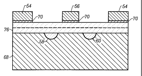
Fig. 10 illustrates a cross-section of an optical device 150 that includes a
polymer buffer layer 152 that reduces DC drift according to the present
invention. In
one embodiment of the present invention, the optical device 150 is formed from
a Z-cut
LiNbO3 substrate 151 and is suitable for high-speed applications. Waveguides
154 are
formed in the LiNbO3 substrate 151 as described above. A conductive polymer
buffer
layer 152 is formed on top of the LiNbO3 substrate 151 as described above.
Ground
electrodes 156 and hot electrode 158 are also formed as described above.
The conductive buffer layer 152 shown in Fig. 10 performs two functions. First
the buffer layer 152 increases the velocity of the microwave signal because
the
dielectric constant of the buffer layer is less than the dielectric constant
of the LiNbO3
substrate 151. This reduces velocity mismatch between the microwave signal and
the
optical signal in a traveling wave modulator. Second the buffer layer 152
bleeds off
CA 02368726 2001-09-26
WO 00/63743 PCT/US00/09997
-16-
unwanted charges and thus reduces DC drift. Reducing DC drift is particularly
important for Z-cut LiNbO3 as described above.
The conductivity of the buffer layer is selected to meet two simultaneous
requirements. First, the conductivity must be low enough to prevent excessive
optical
loss. Second, the conductivity must high enough to reduce DC drift to an
acceptable
level. Some polymers are conductive and other polymers can be made conductive
by
numerous techniques known in the art. One technique includes altering the
material
properties of the polymer to increase electrical conductivity. Another
technique
includes adding at least one substance that increases conductivity. As
described above,
the device of Fig. 10 is relatively inexpensive to manufacture because the
conductive
polymer buffer layer can be fabricated by a spin coating process, which is
much less
expensive compared to the cost of a CVD or sputtering processes.
Fig. 11 illustrates a cross-section of an optical device 160 that includes a
polymer buffer layer 152 and a charge bleed-off layer 162 according to the
present
invention that simultaneously reduces DC drift and bleeds off pyroelectric
charge. In
one embodiment of the present invention, the optical device 160 is formed from
a Z-cut
LiNbO3 substrate 151 and is suitable for high-speed applications. Waveguides
154 are
formed in the LiNbO3 substrate 151 as described above.
The polymer buffer layer 152 is formed directly on top of the LiNbO3 substrate
as described above. The polymer buffer layer 152 may be conductive or slightly
conductive as described in connection with Fig. 10. The charge bleed-off layer
162 is
formed on top of the polymer buffer layer 152. Ground electrodes 156 and hot
electrode 158 are also formed on top of the buffer layer as described above. A
conductive layer 164 may be formed on a bottom surface 166 of the substrate
151.
The charge bleed-off layer 162 comprises a conductive film. Numerous types of
conductive films known in the art may be used. For example, the charge bleed-
off layer
162 may be a metal oxide, a semiconductor like amorphous silicon, or a
conductive
CA 02368726 2001-09-26
WO 00/63743 PCT/USOO/09997
-17-
polymer. The thickness and conductivity of the charge bleed-off layer are
selected to
prevent significant RF current from travelinQ through it. In one embodiment of
the
present invention, the charge bleed-off layer 162 is several hundred Angstroms
thick.
Fig. 12 illustrates a cross-section of an optical device 170 that includes a
polymer buffer layer 152 and a semiconductor charge bleed-off layer 172
according to
the present invention that simultaneously reduces DC drift and bleeds off
pyroelectric
charge. In one embodiment of the present invention, the optical device 170 is
formed
from a Z-cut LiNbO3 substrate 151 and is suitable for high-speed applications.
Waveguides 154 are formed in the LiNbO3 substrate as described above.
The semiconductor charge bleed-off layer 172 is formed directly on the LiNbO3
substrate. In one embodiment of the invention, the semiconductor bleed-off
layer 172
comprises a silicon (Si) layer. Using a silicon charge bleed-off layer is
advantageous
because it simplifies the fabrication process. It is relatively easy to
evaporate silicon by
electron beam evaporation.
The polymer buffer layer 152 is formed on top of the semiconductor charge
bleed-off layer 172 as described in connection above. In one embodiment, the
polymer
buffer layer 152 is slightly conductive as described in connection with Fig.
10 to reduce
DC drift. In another embodiment of the invention, a second charge bleed-off
layer 173
is deposited on top of the polymer buffer layer 152. The second charge bleed-
off layer
173 may be a semiconductor charge bleed-off layer or a metal oxide charge
bleed-off
layer. Ground electrodes 156 and hot electrode 158 are also formed on top of
the buffer
layer as described above. A conductive layer 164 may be formed on a bottom
surface
166 of the substrate 151.
The optical device of Fig. 12 has numerous advantages over the prior art.
Using
a silicon bleed-off layer is advantageous because it simplifies the
fabrication process
and reduces the cost to manufacture the device as described above. The
technology for
depositing amorphous silicon is well known in the art. Another advantage of
the optical
CA 02368726 2001-09-26
WO 00/63743 PCT/US00/09997
-18-
device of Fig. 12 is that constructing an optical device with a buffer layer
on top of a
semiconductor bleed-off layer reduces the diffusion of electrode metal into
the charge
bleed off layer. The device of Fig. 12 has been shown to have relatively low
optical
loss notwithstanding the fact that most semiconductor layers have a high
optical
refractive index and modest optical absorption.
Equivalents
While the invention has been particularly shown and described with reference
to
specific preferred embodiments, it should be understood by those skilled in
the art that
various changes in form and detail may be made therein without departing from
the
spirit and scope of the invention as defined by the appended claims.