Note: Descriptions are shown in the official language in which they were submitted.
CA 02368945 2002-O1-21
Optical Waveguide Device Having Low lnsertion Loss
Inventor: Guomin Yu
Address: 231 - 740 Springland Drive, Ottawa, ON, Canada, K1 V 6L8
Telephone: 613 - 731 - 6473
Email: .~~;~ ~ ~ ~~ ~.,o~ gnu; ~ , (x, ~~-~,
I . Field of the invention
This invention is related to a technique to reduce the insertion loss of ~~n
optical
waveguide device that have one or more waveguides at its input port and an
array of
waveguides at its output port, namely star coupler or sputter.
2. Description of the invention
For conventional star coupler (Fig. l ), the total insertion loss is dominated
by the loss
occurring at the junction between the waveguide array and the slab waveguide
(the
tapered waveguide in sputter is a sort of slab waveguide) due to the
separation of
waveguide in the output waveguide array immediately adjacent to slab. The
smaller the
separation, the less the insertion loss. For example, when the separation is
about 2pm
(1 pm = 10-6m), the insertion loss is about 0.8dB for On = 0.01 at wavelength
I.SSp,m,
and when the separation is about 4 pm, the insertion loss is about I.SdB.
To reduce this insertion loss, two approaches can be used, I) reducing the
separation
of waveguide; 2) reducing the confinement of the waveguide. With reducing
confinement,
the mode size of waveguide becomes bigger. Therefore, for the same separation
of
waveguide, the gap between modes of two waveguides is reduced, which is e~uiv
:lent to
1
CA 02368945 2002-O1-21
reducing the separation.
In this invention, the insertion loss of star coupler or splitter is
substantially reduced
by including a transition region immediately adjacent to the slab between the
output
waveguide array and the slab waveguide. 1'he transition region includes: (1) a
number of
silica paths that intersect the waveguide array; 2) segmented waveguides
connected to
slab and each silica path; and 3) segmented waveguides beyond silica paths
(Fig. 2).
Since the segmented waveguide expands its mode size, which is equivalent to
reducing
the confinement of waveguide, the insertion loss of star coupler having such a
transition
region is reduced from about I.SdB to about 0.3dB with separation of 4 pm in
the output
waveguide array immediately adjacent to the slab for On = 0.01 at I.SSpm
wavelength.
The yield of the optical device also increases by introducing a big feature
size of 4pm in
the transition region.
3. Brief description of the drawings
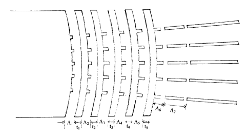
Fig. 1 shows a conventional star coupler.
Fig. 2 discloses a star coupler having a transition region comprising: 1 )
silica paths; 2)
segmented waveguides connected to slab and each silica path; 3) segmented
waveguides
beyond silica paths.
Fig. 3 is a magnified view of the output transition region of the star coupler
shown in
Fig. 2.
Fig. 4 discloses an arrayed waveguide grating (AWG) utilizing the invented
star
coupler.
2
CA 02368945 2002-O1-21
Fig. 5 discloses a branch power sputter having a transition region to achieve
low
insertion loss.
4. Reference cited
US PATENT DOCUMENTS
5,745,618 Apr. 28, 1998, Yuan P. Li, et al, Optical device having low
insertion loss.
5,577,141 . Nov. 19, 1996, Renen Adar, et al, Two-dimensional segmer~~atao~a
mode
tapering for integrated optic waveguides.
4,904,042 Feb. 27, 1990, Dragone, N times N optical star coupler.
OTHER PUBLICATIONS
Z. Weissman, et al, "Analysis of Periodically segmented waveguide mode
expanders",
Journal of Lightwave Technology, Vol. 13, No. 10, Oct. 1995, p2053.
Z. Weissman, et al, "Modes of periodically segmented waveguides", Journal of
Lightwave Technology, Vol. 11, No. 11, Nov. 1993, p1831.
Z. Weissman, et al, "2-D mode tapering via tapered channel waveguide
segmentation", Electronics Letters, Vol. 28, No. 16, Jul. 30, 1992, p1514.
3