Note: Descriptions are shown in the official language in which they were submitted.
CA 02369042 2001-10-O1
WO 00/60414 PCT/US00/07509
SEMICONDUCTOR WAFER PROCESSING SYSTEM WITH VERTICALLY-
STACKED PROCESS CHAMBERS AND SINGLE-AXIS DUAL-WAFER TRANSFER
SYSTEM
INVENTORS
Richard Norman Savage
Frank Steve Menagh
Helder Rodrigues Carvalheira
Philip Andrew Troiani
Dan Lester Cossentine
Eric Robert Vaughan
Bruce Edwin Mayer
CROSS REFERENCE TO RELATED APPLICATIONS
This application claims priority to U.S. Provisional Patent Application Serial
No.
60/127,532 filed April 2,,1999, entitled NEAR ATMOSPHERIC CVD SYSTEM WITH
VERTICALLY-STACKED PROCESS CHAMBERS.
This application also claims priority to U.S. Provisional Patent Application
Serial No.
60/127,650 filed April 2, 1999, entitled SINGLE-AXIS DUAL-WAFER TRANSFER
SYSTEM.
BACKGROUND OF THE INVENTION
Field of the Invention
This invention relates generally to semiconductor wafer processing systems,
apparatuses, and methods. In particular, the present invention relates to a
structure with
vertically-stacked process chambers which minimize the footprint while
maximizing
throughput of a semiconductor wafer processing system. For example, the
present invention
may be used to translate wafers within a near-atmospheric chemical vapor
deposition (CVD)
system, a rapid thermal oxidation system, or other types of wafer processing
systems. The
invention also particularly relates to a wafer transfer apparatus and method
that moves
semiconductor wafers between a loadlock chamber and a process chamber using a
unitary
transfer arm which pivots about a single rotational axis.
CA 02369042 2001-10-O1
WO 00/60414 PCT/US00/07509
-2-
Description of Related Art
Conventionally, wafer transfer between loadlock chambers and process chambers
is
performed by complex apparatus. The complexity of the machinery has resulted
in high cost
of the apparatus, slow wafer processing and a short mean time between
failures.
One example of a conventional wafer processing system is U.S. Patent No.
4,934,315
to Linnebach et al. for "System for Producing Semiconductor Layer Structures
By Way of
Epitaxial Growth". This multiple reactor chamber system accepts wafers for
processing,
where the wafers are loaded into respective holders in an atmospheric handler.
The holders
and wafers are stacked in a load chamber where each holder, carrying its
respective wafer,
is subsequently transferred along a linear path through the multiple reactor
chambers. The
reactor chambers are horizontally aligned along the linear path.
U.S. Patent No. 4,822,756 to Hirayama for "Reaction Furnace and Method of
Operating the Same" discloses a reaction furnace including a wafer support
boat which rolls
from an elevator capsule through a loading chamber and into a treatment
chamber. Although
the loading chambers and the treatment chambers appear to be stacked in a
vertical direction,
the pressure gas system and vacuum system are horizontally disposed from the
treatment
chambers and thus disadvantageously increases the footprint of the reaction
furnace.
U.S. Patent No. 4,423,701 to Nath et al. for "Glow Discharge Deposition
Apparatus
Including a Non-Horizontally Disposed Cathode" discloses a multiple chamber
glow
discharge deposition apparatus having deposition chambers which vertically
orient the wafers
or substrates for processing. The deposition chambers are shown to be
horizontally oriented
with respect to one another. A rotatable arm expels the substrates from the
chamber such that
the arm pushes the substrates in one direction along channeled guides.
U.S. Patent No. 4,816,098 to Davis et al. for "Apparatus for Transfernng
Workpieces" discloses a system in which wafers are loaded onto the system in a
vacuum
wafer carrier which is held under vacuum to reduce contamination of the
wafers. The wafers
are transferred into a cluster tool having multiple process modules via a
vacuum loadlock and
a 2-axis robot arm which only has the capability of transporting a single
wafer at a time.
U.S. Patent No. 5,664,254 to Ohkura et al. for "Substrate Processing Apparatus
and
Substrate Processing Method" discloses a stacking arrangement for a plurality
of process
units. Although the process units may be vertically stacked, only one main
handler is
CA 02369042 2001-10-O1
WO 00/60414 PCT/US00/07509
-3-
provided for transfernng substrates to each of the process units, whereby the
throughput of
each process unit cannot be maximized. The patent also discloses a plurality
of holding arms
arranged in a 3-stage structure for transferring a substrate or wafer. The
holding arms are
mounted on the main handler and are actuated by a complex arrangement
including a vertical
S drive shaft and motor in combination with a horizontally oriented convey
base having a drive
motor and belt to actuate each holding arm.
U.S. Patent No. 5,058,526 to Matsushita et al. for "Vertical Load Lock Reduced-
Pressure Type Chemical Vapor Deposition Apparatus" discloses a
loading/unloading
chamber which is similar to a loadlock chamber found in a conventional cluster
tool. A
cooler including refrigerant-circulating tubes located in an unloading part of
a
loading/unloading chamber cools the treated wafers.
U.S. Patent No. 5,664,925 to Muka et al. for "Batchloader for Load Lock"
discloses
a conventional single-wafer scissor-type transfer arm. Similar conventional
single-wafer
scissor-type transfer arms are disclosed by U.S. Patent No. 5,613,821 to Muka
et al. for
1 S "Cluster Tool Batchloader of Substrate Carner" and U.S. Patent No.
5,607,276 to Muka et
al. for "Batchloader for Substrate Carrier on Load Lock".
U.S. Patent No. 5,778,968 to Hendrickson et al. for "Method for Heating or
Cooling
Wafers" discloses a method for heating or cooling a substrate enclosed vacuum
chamber
using gas having an adjustable pressure above the wafer. Similarly, U.S.
Patent No.
5,5 88,827 to Muka for "Passive Gas Substrate Thermal Conditioning Apparatus
and Method"
discloses a heat transfer plate, located in a thermal conditioning chamber,
which is either
heated or cooled to change the temperature of a substrate.
SUMMARY OF THE INVENTION
A semiconductor substrate or wafer processing system and a substrate or wafer
transfer apparatus in accordance with the present invention overcomes the
disadvantages of
conventional systems discussed above. In accordance with the present
invention, a
semiconductor waferprocessing system includes a mufti-chamber module, the
mufti-chamber
module having a plurality of vertically-stacked loadlock-process chamber
assemblies, an
atmospheric-pressure front end unit having an atmospheric-pressure front end
robot for
transporting semiconductor wafers between a wafer cassette and the loadlock-
process
CA 02369042 2001-10-O1
WO 00/60414 PCT/US00/07509
-4-
chamber assemblies, a common process chemical delivery system for each stack
of chamber
assemblies, and a dedicated wafer transfer apparatus for each loadlock-process
chamber
assembly. The processing system may also include two or more mufti-chamber
modules
oriented in a linear array. A loadlock chamber is dedicated to each process
chamber, the
chambers together forming a respective loadlock-process chamber assembly. A
cooling plate
is disposed within each loadlock chamber below a single-pivot transfer arm of
the wafer
transfer apparatus. The cooling plate is provided with lift pins for removing
wafers from the
pivot transfer arm. A wafer chuck assembly having a chuck clamping surface and
pins is
provided within each process chamber for positioning wafers within the process
chamber.
In one embodiment of the present invention, the wafer chuck assembly
translates a wafer
within the process chamber past a chemical vapor deposition injector for
processing.
One wafer transfer apparatus serves each loadlock-process chamber assembly.
Each
wafer transfer apparatus includes a transfer arm adapted to carry and transfer
two or more
wafers between the loadlock chamber and the process chamber. The transfer arm
pivots
1 S about a single pivot axis extending through the loadlock chamber. The
transfer apparatus has
the capacity to simultaneously carry two wafers between the loadlock chamber
and the
process chamber. The wafer transfer apparatus also includes a retracted/home
position and
an extended position, wherein the single pivot axis allows the transfer arm to
pivot between
the retracted and extended positions. The cooling plate is disposed below the
pivot arm when
the pivot arm is in the retracted position. The wafer transfer apparatus also
includes a lower
wafer shelf and an upper wafer shelf integrated within the transfer arm.
Another aspect of the present invention is directed to a method of
transferring the
unprocessed wafer from the loadlock chamber to the process chamber,
transferring the
unprocessed wafer from the upper wafer shelf to a semiconductor wafer chuck
mounted in
the process chamber, translating the semiconductor wafer chuck from a
retracted position,
to an extended position where the wafer is processed, simultaneously
transferring the
processed wafer and a second unprocessed wafer between the loadlock chamber
and the
process chamber, and transfernng the processed wafer from the lower wafer
shelf to the
cooling plate.
It is an object of the present invention to provide a wafer processing system
having
multiple loadlock-process chamber assemblies, each assembly having one
loadlock chamber
CA 02369042 2001-10-O1
WO 00/60414 PCT/US00/07509
-S-
dedicated to a process chamber and a dedicated transfer arm which moves wafers
between
respective loadlock and process chambers.
It is an object of the present invention to vertically stack two or more
loadlock-
process chamber assemblies to form a mufti-chamber module in order to reduce
the system
footprint and thus optimize the vertical orientation and layout of the
loadlock-process
chamber assembly stacks.
It is another object of the present invention to align the mufti-chamber
modules in a
linear fashion with a single atmospheric-pressure front end wafer transfer
system delivering
substrates to all loadlock chambers to optimize the footprint of the
processing system.
It is another object of the present invention to provide a common process
chemical
delivery system and local control system for each mufti-chamber module.
It is another obj ect of the present invention to optimize wafer flow paths
and process
timing for a linear array, vertically-stacked processing system and method in
order to
maximize throughput of each process chamber and of the full processing system.
It is another object of the present invention to optimize the number of
process
chambers within a footprint to increase processing system throughput.
It is a further object of the present invention to provide a new wafer
transfer arm and
wafer transfer method which moves semiconductor wafers from a single
atmospheric-
pressure front end robot, through a loadlock chamber, and into a wafer process
chamber, in
which the transfer arm pivots about a single rotational axis with one pivot
point located on
the transfer arm to side-load the process chamber.
It is another object of the present invention to provide a transfer arm having
the
capacity to carry two wafers in order to facilitate and expedite wafer
transfer between the
loadlock chamber and the process chamber. In particular, it is an object of
the present
invention to provide a transfer arm which has the capacity to carry an
unprocessed wafer and
a processed wafer at the same time in order to maximize system throughput.
It is another obj ect of the present invention to provide a wafer.cooling
plate to reduce
wafer cooling time after a wafer is processed to facilitate wafer transfer out
of the loadlock
and into a cassette maximizing parallel steps within the processing system and
thus
increasing throughput of the processing system.
CA 02369042 2001-10-O1
WO 00/60414 PCT/US00/07509
-6-
BRIEF DESCRIPTION OF THE DRAWINGS
The foregoing and other obj ects of the invention will be more clearly
understood from
the following description when taken in conjunction with the accompanying
drawings of
which:
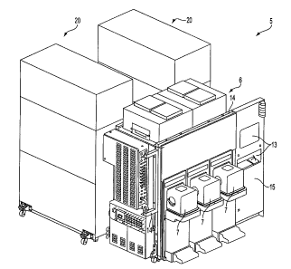
Figure 1 is a perspective view of a processing system in accordance with the
present
invention.
Figure 2 is a plan view of the processing system shown in Figure 1.
Figure 3 is a perspective view of a mufti-chamber module in accordance with
the
present invention:
Figure 4 is a diagrammatic illustration showing a wafer flow path diagram of a
conventional cluster tool system.
Figure S is a diagrammatic illustration showing a wafer flow path diagram of
the
processing system shown in Figure 1.
Figure 6 is a perspective view of a loadlock chamber and a transfer arm in an
1 S extended position holding two wafers.
Figure 7 is a perspective view of the loadlock chamber shown in Figure 6 with
the
cover removed to show the transfer arm in a retracted home position.
Figure 8 is a perspective view of the load lock chamber similar to Figure 6
including
a support structure but without wafers.
Figure 9 shows a perspective view of transfer arm similar to the one shown in
Figure
6 carrying two wafers.
Figure 10 is a perspective sectional view of the process chamber of Figure 2
taken
along line 10-10 of Figure 2.
Figure 11 is a perspective sectional view of the process chamber of Figure 2
taken
along line 11-11 of Figure 2.
Figure 12 is a perspective sectional view of a loadlock-process chamber
assembly
including the loadlock and process chambers of Figure 2 taken along line 12-12
of Figure 2.
Figure 13 is a diagrammatic illustration showing an exemplary common chemical
delivery system.
Figure 14 is a plan view of an alternative embodiment of the processing system
according to the present invention.
CA 02369042 2001-10-O1
WO 00/60414 PCT/US00/07509
_7_
Figure 15 is a perspective view of an alternative embodiment of the processing
system
according to the present invention.
Figures 16(a) through 16(1) schematically show a wafer transfer sequence in
accordance with the presentinvention.
Figure 17 is a diagrammatic illustration showing comparative analytical
calculations
for an exemplary 200 mm wafer full-stroke architecture for several parameters
in accordance
with the present invention.
DESCRIPTION OF THE PREFERRED EMBODIMENTS
Reference will now be made in detail to the preferred embodiments of the
invention,
examples of which are illustrated in the accompanying drawings. While the
invention will
be described in conjunction with the preferred embodiments, it will be
understood that they
are not intended to limit the invention to those embodiments. On the contrary,
the invention
is intended to cover alternatives, modifications and equivalents, which may be
included
within the spirit and scope of the invention as defined by the appended
claims.
The present invention is directed to a new processing system for processing
semiconductor wafers or substrates. It is noted that the term "wafers" is
intended to refer to
both wafers and substrates for the purposes of the present invention. The
present invention
is directed to a system, apparatus, and method which maybe used in conjunction
with various
wafer processes including, but not limited to, near-atmospheric chemical vapor
deposition
(CVD) or rapid thermal oxidation processes. In the case that such CVD
processes are
utilized, the CVD processes may include deposition processing pressures
generally between
about 5 Torr and about 760 Ton, more typically between about 100 Torr and
about 700 Torr,
and usually between about 200 Torr and 600 Torr. One should appreciate that
the process
chambers of the present invention may also operate at lower vacuum pressures
in the milli-
Torr regime. For example, the addition of suitable vacuum pumps would allow
the present
invention to operate in the 10 m Torr to 200 m Torr range, and more generally
in the 10 m
Torr to 5 Torr range.
Referring to Figures 1-3, the major components of the semiconductor wafer
processing system 5 of the present invention include an atmospheric-pressure
front end
(AFE) unit 6, a multi-chamber module (MCM) 20 having vertically stacked sets
of process
CA 02369042 2001-10-O1
WO 00/60414 PCT/US00/07509
_g_
chambers 40, a common process chemical delivery system 24 and a common control
system
21 which are shared by sets of stacked process chambers 40, and loadlock
chambers 80 for
semiconductor wafer transfer between a respective process chamber 40 and the
atmospheric-
pressure front end unit 6.
Atmospheric-pressure front end unit 6 is located at the front of wafer
processing
system S and is coplanar with a clean room wall (not shown). Atmospheric-
pressure front
end unit 6 includes one or more wafer cassettes or load ports 7. Such wafer
cassettes are
conventional and known in the art. An AFE robot 8 transfers wafers between
cassettes 7, a
wafer aligner 9 (not shown in Figures 1-3 but shown in Figure 14), and
loadlock chambers
80. Robot 8 returns wafers to their respective cassettes 7 on completion of
processing. The
wafer aligner is provided for wafer centering and notch alignment prior to
transfernng the
wafers into loadlock chambers 80. These components are housed in a rigid frame
14 which
defines a clean environment with the appropriate environmental air handling
equipment. The
front surface of the AFE unit 6 incorporates the system facade 15, which also
supports a user
interface panel and display 13.
Referring to Figures 2 and 12, one loadlock chamber 80 is provided for each
process
chamber 40. Loadlock chamber supports 89, shown in Figure 8, position each
loadlock
chamber 80 relative to a respective process chamber 40. Wafers are moved
between AFE
unit 6 and each process chamber 40 through a respective loadlock chamber 80. A
front end
gate valve 10 connects each loadlock chamber 80 and AFE unit 6. Front end gate
valve 10
also hermetically seals loadlock chamber 80 from AFE unit 6 such that loadlock
chamber 80
maybe evacuated. A process chamber slot valve 41 is likewise provided
connecting loadlock
chamber 80 to a respective process chamber 40. Process chamber slot valve 41
hermetically
seals process chamber 40 from loadlock chamber 80 such that loadlock chamber
80 may be
vented to atmospheric-pressure without disturbing the pressure of process
chamber 40.
Central to the present invention is the concept of providing each process
chamber
with its own dedicated loadlock chamber and wafer transfer arm to maximize the
throughput
both of each process chamber and that of the entire processing system. The
present invention
further ensures maximum throughput of the processing system in situations
where substrate
processing requires time to cool wafers after processing.
Typically, a loadlock serves as a buffer between two different environments,
for
CA 02369042 2001-10-O1
WO 00/60414 PCT/US00/07509
-9-
example, between a room temperature, atmospheric-pressure environment and an
elevated
temperature, evacuated environment. Thus, the loadlock requires some non-zero
operating
time to adjust the environment of the loadlock chamber to first match one
environment in
which the loadlock can accept a substrate and then to subsequently match a
second
S environment to transfer the substrate to a process chamber. Although no
substrate processing
is performed in the loadlock, the substrate must "wait" or spend some non-zero
time within
the loadlock chamber. Typically, this time is on the order of tens of seconds,
and possibly
as much as several minutes.
Prior art approaches as illustrated in Figure 4 typically include a front end
robot that
delivers substrates to one or more loadlocks. A second robot, often in a
chamber hub, then
transports substrates between any one of the loadlocks and any one of several
process
chambers. The front end robot may be used to transport substrates to an
aligner prior to
entering a loadlock, however, the central hub robot may instead transport the
substrate from
a loadlock to an aligner prior to transferring the wafer to a process chamber.
Regardless,
1 S each robot has responsibility for distribution of wafers between multiple
modules. Software
scheduling is possible for prior processing systems using two robots and is
often used in prior
art approaches. However, as indicated in Figure 4, the scheduling can be quite
complex.
Figure 4 illustrates an example of a prior art wafer flow path diagram
corresponding
to a prior art processing system which includes four load cassettes CASS l,
CASS 2, CASS
3, CASS 4, a Front End Robot, four loadlock chambers LL1 UPPER, LL1 LOWER, LL2
UPPER, LL2 LOWER, a Central Hub Robot, and four process chambers PM1, PM2,
PM3,
PM4. Because a single central hub robot transfers the wafers between all the
loadlock
chambers and all the process chambers, the number of possible wafer flow paths
in such a
system totals sixty-four (64). For example, four possible "load cassette/front
end robot"
paths multiplied by four possible "front end robot/loadlock/central hub robot"
paths
multiplied by four possible "central robot/process chamber" paths equals sixty-
four (64)
possible paths.
In some applications, processed wafers may need to be cooled prior to being
returned
to the load cassettes. Prior art practice typically includes one or more
cooling chambers, or
"wait" positions where wafers may sit and cool, that are within reach of the
central hub robot
only. Limiting transportation of hot wafers within the reach of only the
central hub robot
CA 02369042 2001-10-O1
WO 00/60414 PCT/US00/07509
-10-
minimizes the apparatus requiring special materials to handle hot wafers (for
example, end
effectors, wafer holders and surfaces, cassettes, etc.), and thus minimizes
cost.
However, the addition of a cooling chamber or a position where the wafer must
"wait" and cool further complicates the scheduling of wafers moved by the
central hub robot,
and thus also complicates the scheduling of the central hub robot with respect
to that of the
front end robot. Typically, the front end robot and the central hub robot each
can transport
wafers very quickly. However, each robot is paced by the "readiness" of the
wafers, and
scheduling optimization of such prior art systems thus requires very precise
timing and
requires extensive feedback and/or "look ahead" prediction regarding
utilization of the
various process chambers and loadlocks to minimize "waiting" times and thus to
ensure
highest throughput through the system. Often, in practice, even the slightest
pause in wafer
transfer to one process chamber (or loadlock) can disrupt overall wafer flow
throughout the
whole system. Schedulers may purposely include slight delays in scheduling
programs to
accommodate these slight potential delays at the cost of less than optimal
throughput. In
short, synchronization between the two robots that must choose among several
multi-
accessible wafer locations, including the load cassettes, loadlocks, and
process chambers, is
key to maintaining acceptable throughput, but such synchronization is very
complex.
In contrast, the present invention employs one robot at the front end of the
system to
distribute substrates to one or more loadlock chambers, each dedicated to a
respective process
chamber. Each loadlock chamber includes a dedicated individual transfer arm
for moving
substrates between the dedicated loadlock chamber and the respective process
chamber.
Figure 5 illustrates a flow path diagram corresponding to a processing system
in accordance
with the present invention. Because each process chamber now has a dedicated
loadlock
chamber and transfer arm rather than having to share loadlock chambers and a
central robot
as in the prior art, scheduling the flow of wafers is significantly less
complex because
possible number of wafer flow paths is significantly reduced from that of the
prior art.
As shown in Figure 5, a processing system in accordance with the present
invention
has an equal number of process chambers as that of the prior art shown in
Figure 4. However
the present invention dedicates a loadlock chamber to each process chamber
thus providing
four loadlock-process chamber assemblies LL/PM1, LL/PM2, LL/PM3, and LL/PM4
and
eliminating the need for a central hub robot. Thus, the number of possible
wafer flow paths
CA 02369042 2001-10-O1
WO 00/60414 PCT/US00/07509
-11-
is reduced from the sixty-four (64) paths of the prior art to sixteen ( 16)
paths of the present
invention. For example, four possible "load cassette/front end robot" paths
multiplied by
four possible "front end robot/loadlock-process chamber assembly" paths equals
sixteen ( 16)
possible paths. Accordingly, scheduling of the present invention is less
complex because
S there are far fewer path options to manage. The front end robot delivers
wafers to one of four
(in this example) loadlock chambers, and once placed in a loadlock chamber, a
wafer's path
into and out of a process chamber is fixed and independent of any other
wafer's path.
In accordance with the present invention, the lengthy process of loadlock
environmental changes and process chamber processing are contained in
individual loadlock-
process chamber assemblies, each including a loadlock chamber, a transfer arm,
and a
process chamber. The present invention allows parallel processing of
substrates because it
establishes parallel paths between the respective loadlocks and process
chambers, as
represented by arrows ARM in Figure 5. The complexity in scheduling is thus
reduced
because the addition of dedicated loadlock chambers and transfer arms enables
independent
and parallel processing of the substrates.
Another important attribute of the present invention is the addition of
dedicated
hardware for each loadlock-process chamber assembly that is sufficiently
simple in design
to be cost effective despite its duplicity. Because each process chamber has
its own loadlock
chamber, a wafer transfer plane within each loadlock-process chamber assembly
is
established that is simple and relatively constant. Hence, a transfer arm
having a single
translation axis can be employed to transfer a wafer between each loadlock
chamber and a
respective process chamber. Further, overall tool footprint can be reduced
when a front end
robot has a vertical span capable of reaching the transfer planes of multiple
stacked loadlock-
process chamber assemblies. Thus, the present invention preferably includes or
is used in
conjunction with a single front-end robot having mufti-axis capability
including an
appropriate vertical span and with multiple low-cost single axis transfer
arms.
One aspect of the present invention which allows dedication of one loadlock
chamber
80 to each process chamber 40 is the provision of a cooling plate 95, Figure
7, within each
loadlock chamber 80. Another aspect of the present invention which allows such
dedication
is the provision of a dual-wafer single-arm loadlock transfer arm 82, Figure
6, which has the
capability to transport two wafers simultaneously, including one unprocessed
wafer and one
CA 02369042 2001-10-O1
WO 00/60414 PCT/US00/07509
-12-
processed wafer. Significant cost improvement is obtained with the
configuration of the
present invention because only one translation axis is controlled through the
control system
for each process chamber. As shown in Figures 7 and 8, transfer arm 82 only
rotates about
transfer arm pivot axis 83, thus only a single uncomplicated angular motion of
transfer arm
82 about pivot axis 83 need be controlled by the control system.
Referring to Figures 7 and 8, a wafer cooling plate 95 is mounted inside
loadlock
chamber 80. A monolithic single-axis loadlock transfer arm 82 (theta-axis
rotation) with a
dual-wafer effector end 84 is also provided which allows vertical coaxial
placement of two
wafers on end effector 84. Transfer arm 82 has a single servo axis or pivot
axis 83 and is
operated by a single servo mechanism such as transfer arm drive motor assembly
79. End
effector 84 is a U-shaped component allowing an unprocessed wafer to be placed
on an upper
wafer shelf 85 of end effector 84 and a another processed wafer placed on
lower wafer shelf
87. The shelves are defined by horizontal plates forming shelves 85, 87 and
include
supporting waferedge supports 86, 88 on the open portion of end effector 84.
Transfer arm 82 has a home position, as shown in Figure 7, in which transfer
arm 82
is located entirely within loadlock chamber 80 awaiting delivery of an
unprocessed wafer
from front end robot 8, or awaiting removal of a processed wafer by cooling
plate lift pins
96, as discussed below. Wafer cooling plate 95 is integrated into loadlock
chamber 80 for
cooling processed wafers before they are removed from loadlock chamber 80 by
AFE robot
8 to minimize wafer transfer failures resulting from thermally-warped wafers
and cassette
material failures from high-temperature post-processed wafers. Cooling plate
95 is mounted
below transfer arm 82 and is concentrically oriented with respect to wafers
mounted on the
upper and lower wafer shelves 85, 87. Cooling plate 95 may be liquid cooled or
air cooled
or inert gas cooled to ambient temperatures. For example, water at about
18°C to 25°C may
be circulated through cooling plate 95 to regulate the temperature thereof.
One should
appreciate that other suitable liquid temperature ranges may be used. In the
case that cooling
plate 95 is liquid cooled, the cooling liquid may be circulated through
cooling plate 95, chuck
assembly 60, and the walls of process chamber 40 for temperature regulation
thereof.
Cooling plate 95 is equipped with cooling plate lift pins 96 which may elevate
wafers
resting on lower wafer shelf 87 when loadlock transfer arm 82 is located in
the home
position. The height of cooling plate lift pins 96 is controlled by a cooling
plate lift pin
CA 02369042 2001-10-O1
WO 00/60414 PCT/US00/07509
-13-
actuator 97, shown in Figure 8. Once a wafer is elevated, loadlock transfer
arm 82 pivots
away from the home position to an extended position, shown in Figures 6 and 8,
leaving the
wafer behind on cooling plate lift pins 96. The wafer is then lowered to the
cooling plate in
order to cool the disc. Alternatively, the wafer may be lowered to a position
slightly above
cooling plate 95 such that the wafer is cooled without contacting plate 95
thus minimizing
wear and thermal stress on the wafer. One should appreciate that various types
of cooling
may be implemented including conductive, convective, or radiative cooling.
In a similar fashion, cooling plate lift pins 95 extend to elevate a wafer
above the
level of upper water shelf 85 and then lower to load the wafer on shelf 85
once transfer arm
85 returns to its home position. As noted above, cooling plate lift pin
actuator 97 controls
lift pins 96. Cooling pin actuator 97 is located external to loadlock chamber
80 to minimize
the dimensions of loadlock chamber 80. For example, a linear solenoid or other
known linear
actuators may be mounted external to loadlock chamber 80. A bellows (not
shown) is used
to interconnect the actuator and cooling pins 96 in a manner to preserve the
evacuated
1 S environment of loadlock chamber 80. Alternatively, one should appreciate
that a cooling pin
actuator could be instead located within the loadlock chamber if so desired.
Regarding the shape of wafer shelves 85, 87, it is noted that upper wafer
shelf 86 is
substantially U-shaped thus allowing transfer arm 82 to retract from its
extended position
while an unprocessed wafer is supported by extended chuck lift pins 70 in the
up position,
as discussed in detail below. In particular, the U-shape of upper wafer shelf
85 prevents lift
pins 70 from contacting upper shelf 85 or the transfer arm 82. In contrast,
lower wafer shelf
87 only supports a wafer on opposing sides of the wafer by lower wafer
supports 88, as
shown in Figures 9 and 12. As shown in Figure 12, the base of the U-shape of
lower wafer
shelf 87 is open thereby allowing transfer arm 82 to extend from its
retracted/home position
while a processed wafer is supported by extended cooling plate lift pins 96 in
their up
position.
Referring now to Figure 10, an exemplary process chamber 40 is shown. In this
embodiment, process chambers 40 may incorporate a chemical vapor deposition
(CVD)
linear injector 43 assembly such as, for example, a MultiBlokT"' linear
injector of the type
made by the Silicon Valley Group Thermal Systems, Scotts Valley, California
and further
described in U.S. Patent Application Serial No. 09/113,823 (Attorney Docket
No. A-59471-
CA 02369042 2001-10-O1
WO 00/60414 PCT/US00/07509
-14-
4), filed July 10, 1998, the entire disclosure of which is incorporated herein
by reference.
Each CVD linear injector assembly 43 employs linear inj ectors 44, 45 for
processing 200 mm
wafers. Alternatively, three linear inj ectors may be employed in a single CVD
linear inj ector
assembly for processing 300 mm wafers. However, one should appreciate that
other types
S of process chambers could also be utilized in accordance with the present
invention. For
example, a process chamber in which films are grown and annealed at elevated
temperatures
could also be used either in combination with or instead of the CVD chambers
discussed
above.
A semiconductor wafer chuck assembly 60 is provided inside each process
chamber
40. Wafer chuck assembly 60 has several basic functions including: ( 1 )
receiving a wafer
from and releasing a wafer to the transfer arm; (2) holding a wafer during
processing; (3)
providing a uniform thermal environment for a wafer depending upon wafer
process
temperatures; and (4) translating a wafer within the process chamber if
required by the wafer
process method. For example, wafer chuck assembly 60 may be provided inside
each process
chamber 40 for preheating, securing, and transporting the wafers relative to
CVD linear
injector assembly 43. Alternatively, chuck assembly 60 may also be used to
cool a wafer
and/or translate the wafer relative to other types of processing tools, such
as material removal
tools.
As shown in Figure 10, wafer chuck 60 includes a clamping surface 62 on which
a
semiconductor wafer is placed. Wafer chuck 60 includes a heating element (not
shown)
which preheats the unprocessed wafer prior to processing by CVD injector 43.
Chuck
insulation 76 is also provided to isolate the heat applied to the wafer. A
hold down clamp
such as a chuck vacuum clamp 63 secures the wafer to chuck assembly 60. Such
vacuum
clamps are well known in the art and are not discussed in detail. One should
appreciate that
other suitable clamping means may also be used such as electrostatic wafer
clamping means.
Generally, a backside of a wafer is vacuum held against a wafer chuck plate 62
of wafer
chuck assembly 60 by a chuck vacuum clamp 63 in a known manner. The vacuum
clamp is
operably connected to a vacuum source by a chuck assembly umbilical chain 59.
Umbilical
chain 59 provides power, control signals, and cooling water to chuck assembly
60 while
allowing it to translate within process chamber 40.
Injector gases are contained within deposition micro-zones or micro-regions,
CA 02369042 2001-10-O1
WO 00/60414 PCT/US00/07509
-15-
indicated generally by the numeral 49, which is defined as the area
immediately under the
linear injector outlets. The top surface of a wafer mounted on wafer chuck
plate is
substantially coplanar with a top surface of seal plates 61, both of which are
adjusted to pass
within approximately 1 mm of the bottom outlets of linear inj ectors 44, 45.
Such placement
S of the wafer defines a low-conductance gas path between deposition micro-
zones 49 and
remainder of process chamber 40. This path is referred to as a micro chamber
isolation
region or the semi-seal region. The 1 mm semi-seal gap is adjusted by
adjusting the position
of a chuck translation frame 64 with respect to injector assembly 43, as
discussed below.
Once the semi-seal gap is set, it does not change during system operation.
In practice, a wafer is placed on chuck surface 62 while the chuck is in a
retracted
or load position, as shown in Figures 10-12. The wafer is positioned over
chuck lift pins 70
which lift the wafer from upper wafer shelf 85. Transfer arm 82 pivots back to
its home
position leaving the wafer on chuck lift pins 70. Next, the wafer is lowered
to the chuck
surface 62. Chuck lift pins 70 raise and lower in unison and are operably
connected to a
chuck lift pin yoke 72. Lift pin yoke 72 is, in turn, operably connected to a
chuck lift pin
linear drive shaft 73 which is actuated by a lift pin servo actuator assembly
74. It should be
appreciated that other means for controlled linear movement may also be used.
For example,
a worm drive could be provided to impart linear motion on chuck lift pin yoke
72 and/or
chuck lift pins 70.
Refernng to Figure 11, the wafer is vacuum-clamped to chuck surface 62. Chuck
assembly 60 translates along chuck guide rails 66 of chuck translation frame
64, past CVD
injector 43, to an extended position. For example, a chuck translation
actuator 67, such as
an electric servo motor, operably drives chuck assembly 60 along chuck guide
rails 66 via
a chuck translation driving screw 68. One skilled in the art would recognize
that other chuck
translation devices may also be used. Thus, the wafer secured to wafer chuck
plate 62 is
translated under the injector outlets of the linear injectors 44, 45 in a
single full-pass stroke
in the direction of arrow A. The single full-pass stroke allows the entire
wafer surface to be
deposited by all the injector outlets (i.e., two injector outlets for a 200 mm
wafer size, or by
three injector outlets for a 300 mm wafer size.) It is noted that the number
of injectors and/or
injector outlets is not dependent on wafer size. The number of injectors
and/or injector
outlets can be varied in order to optimize throughput of process chamber 40.
This full-stroke
CA 02369042 2001-10-O1
WO 00/60414 PCT/US00/07509
-16-
action may be repeated as many times as necessary to produce the desired
processing of the
wafer. The chuck translation speed may also be adjusted according to the
desired thickness
of a Si02 layer formed on the wafer as it passes CVD injector 43. For example,
in one
embodiment of the present invention, the translation speed ranges from about 1
mm/s to
about 60 mm/s. Upon completing deposition, the wafer is translated back to the
load position
where chuck lift pins 70 raise the wafer off wafer chuck plate 62 in
preparation for hand off
to the loadlock transfer arm 82.
The process or reactor chamber 40 employs side doors 54, Figures 11 and 12,
and end
doors 55, Figure 10, to allow easy access for servicing and calibration of the
translation frame
64 and chuck assembly 60 without disturbing the semi-seal gap or deposition
micro-zone,
or any other process chamber components, such as CVD linear injector 43. As
noted above,
the 1 mm semi-seal gap is adjusted by adjusting the position of the chuck
translation frame
64. This is accomplished by adjusting chuck adjusters 69. As shown in Figure
2, each
process chamber 40 is preferably provided with three chuck adjusters 69, two
of which are
also shown,in Figure 10. Such a configuration allows the pitch, roll, and
height of chuck
assembly 60 to be precisely adjusted. For example, chuck adjusters 69 could be
adjusted to
precisely adjust the semi-seal gap in the case that process chamber 40
includes a CVD linear
injector 43. Chuck assembly adjustors 69 could also be used to adjust the
position of a wafer
relative to other processing tools. Such adjusters may take the form of
adjusting screws or
other well known adjusting means. One should appreciate that greater than or
fewer than
three chuck assembly adjusters may also be used. For example, two adjusters
may be used
in which a third point of translation frame 64 is fixed relative to process
chamber 40.
Refernng to Figure 2, process chambers 40 are vertically arranged in pairs to
conserve
tool floor area or footprint requirements. The vertically stacked process
chamber pairs in
combination with a common chemical delivery system 24, and a common control
system 21
are collectively referred to as a multi-chamber module (MCM) 20. The two
process chambers
could be substantially identical, for example, each could contain independent
CVD linear
injectors, wafer chuck assemblies, and chuck translation frames. Furthermore,
each process
chamber includes a respective dedicated loadlock chamber and cooling plate. In
the event
that changes are desired between the two chambers, such differences can be
easily
accommodated without affecting the other.
CA 02369042 2001-10-O1
WO 00/60414 PCT/US00/07509
-17-
Alternatively, different types of process chambers could be included in each
multi-
chamber module. For example, one process chamber 40 could include a CVD linear
injector
43, while another process chamber, vertically stacked with respect to the
first, could include
a rapid thermal oxidation tool (not shown). Furthermore, one should appreciate
that MCM
S 20 may include three process chambers 40 vertically stacked one above the
other, as shown
in Figure 15. Again, one should appreciate that process chambers 40 may take
the form of
a CVD process chamber, as discussed above, or other types of process chambers,
or a
combination thereof.
The spacing between process chambers 40 of MCM 20 depends on specific design
constraints such as maximum front end robot vertical stroke, service access
spacing 23
between the process chambers for the CVD inj ectors and chemical delivery
plumbing, as well
as the overall height of the process chamber as defined by the maximum height
of the chuck
assembly and the translation frame. As shown in Figure 12, chuck lift pin
actuator 71 of the
present invention is located external to process chamber 40 in order to reduce
the overall
height and volume of process chamber 40. Bellows 75 are used between lift pin
actuator 71
and chuck lift pins 70 in order to maintain the particle-free, near-
atmospheric-pressure
environment of process chamber 40.
Vertically stacked process chambers 40 of MCM 20 are located on a common frame
which also supports a common process chemical system 24 and a common local
controls
system 21. Delivery system 24 is located at the top of MCM 20 and provides and
delivers
material to the stacked process chambers 40. For example, delivery system 24
could include
a chemical delivery system for delivering chemicals to the two stacked process
chambers 40
within MCM 20. Common control system 21 may be located within the MCM, below
the
lower process chamber 40. Alternatively, such components could be provided on
a separate
rack alongside the CVD processing system, depending on the quantity and
packaging
requirements of the electronic components and any distance limitations in
achieving
reasonable process and system control. With one delivery system supplying all
process
chambers 40 of each MCM 20, significant cost and space savings can be
achieved. One
should recognize that the actual location of process chemical delivery system
24 and common
control system 21 may vary within the scope of the present invention. For
example, delivery
system 24 could be located below the lower process chamber or between process
chambers.
CA 02369042 2001-10-O1
WO 00/60414 PCT/US00/07509
-18-
Likewise, common control system 21 could be located above upper process
chamber.
An exemplary process chemical delivery system 24 for three stacked process
chambers is shown in Figure 13. Delivery system 24 includes a chemical
delivery system
having a manifold unit 25 for splitting the chemical sources into the CVD
linear injector 43
of three process chambers 40. Alternatively, a manifold unit may be provided
to split the
chemical sources into the injectors of fewer than or greater than three
process chambers. As
such, chemical deposition simultaneously starts and stops in all process
chambers 40 of a
MCM 20. There is no individual means of metering, controlling, or balancing
chemical
delivery between the individual process chambers 40 for wafer processing
operations.
Instead, a source-chemical split point 25 and an oxidizer split point 26
substantially
uniformly distribute the chemical sources and the ozone, respectively, into
the individual
CVD linear injectors 43. Any slight variations in deposition thickness
resulting from
chemical delivery variations between the process chambers 40 are accommodated
byvarying
the wafer chuck translation speed thereof, since each process chamber 40, has
independent
chuck translation actuators 67. Individual metering-valves or flow-controllers
for each
chamber may be provided to individually control chemical source and ozone
delivery into
individual process chambers 43. Thus, allowing each process chamber 43 to
operate
independently of the others. The common delivery system of the present
invention
minimizes overall cost and complexity of the wafer processing system. One
should
appreciate that individual delivery systems, for example individual flow
control valves, may
instead be utilized for each process chamber but such configuration may result
in higher
costs.
One ozone generator is provided for each delivery system 24 of a respective
MCM
20. However, one liquid chemical supply cabinet may be provided for multiple
delivery
systems 24 corresponding to multiple MCMs 20. A similar approach is employed
for
anhydrous HF cleaning systems, when utilized, where one HF system is employed
and
passively split by a manifold unit between all process chambers 40 of one MCM
20.
However, in a variant to the design, if an atomic fluorine generation source
is used to
generate cleaning precursors, then one fluorine generation source is provided
for each process
chamber 40, although the cleaning of all process chambers 40 in one MCM 20
will take place
simultaneously to optimize throughput of process chambers 40 and to simplify
the chemical
CA 02369042 2001-10-O1
WO 00/60414 PCT/US00/07509
-19-
delivery hardware for the fluorine generation source. Alternatively, other
embodiments could
include a single atomic fluorine source for both process chambers in one MCM.
The plan view of the wafer processing system 5 of the present invention is
arranged
such that a series of MCMs 20, e.g., two, three, or more MCMs 20, are arranged
in a linear
fashion in parallel to each other. Such arrangement of MCMs 20 may be
perpendicular to
AFE unit 6, as shown in Figure 3, or an angle, as shown in Figure 14,
according to the
specific design of loadlock chambers 80. As such, wafer processing system 5
may be
considered a "linear array".
One skilled in the art would recognize that several MCMs may be employed using
other geometries around a transport system, such as a circular arrangement
around a central
robot, a mirrored parallel arrangement surrounding a translating central robot
on the left and
right sides of the machine, or other non-linear arrangements where the stacked
chambers may
be employed, provided that a loadlock chamber is provided for each process
chamber.
The configurations of process chambers 40 and MCMs 20 discussed above provide
footprint improvements over similar linear injector cluster tool systems. For
example, as
compared to conventional systems having an equivalent number of process
chambers, for
example, having four process chambers, the footprint is reduced from about 168
square feet
(ftz) for a prior art system to about 73 square feet (ft2) for a system
according to the present
invention. This reduction in footprint is accomplished primarily by stacking
CVD process
chambers 40, and eliminating a distinct transport module hub typically
provided in
conventional cluster tool CVD processing systems, in favor of individual
loadlocks 80
attached to a corresponding CVD process chamber 40 and to the atmospheric-
pressure front
end unit 6. Also, space is more efficiently utilized in the linear array
layout because space
is not lost to a large transport module (TM) chamber and central hub robot
typically present
in conventional systems at the center of a cluster tool system
(diagrammatically shown in
Figure 4).
Footprint areas of CVD processing system of 300 mm applications (e.g. wafers)
according to the present invention are comparable to the footprint areas of
conventional
systems for 200 mm applications. The present invention provides tremendous
advantages
for wafer processing facilities originally designed for 200 mm applications
because such
facilities may incorporate the inventive system for 300 mm applications using
the existing
CA 02369042 2001-10-O1
WO 00/60414 PCT/US00/07509
-20-
floor space of the facility.
The semiconductor wafer processing system, semiconductor wafer transfer
apparatus,
and method of the present invention provide numerous technical benefits. For
example,
production and processing costs, as well as the complexity of the system may
be minimized
by eliminating the need for multiple servo axes to move the wafer. The motion
of the
semiconductor processing apparatus, for example transfer arm 82, is reduced to
a motion
about a single axis, thereby reducing overall wafer automation costs. Use of
the monolithic
single-axis transfer arm also eliminates articulated components in the
transfer mechanism
thus minimizing complexity and potential reliability failures. The single-axis
transfer arm
of the present invention further minimizes particle formation and
contamination because
there are fewer moving parts in the loadlock chambers. The single axis-arm
minimizes the
depth of the overall system by allowing side-loading of the process chambers
and thus
optimizes packaging constraints of the system. Furthermore, by placing a
cooling plate in
each loadlock chamber, there is no need for a dedicated separate cooling
station. The cooling
1 S plate arrangement of the present invention does not require additional
transfer arm axes since
it employs cooling plate lift pins for wafer removal of wafers from the
transfer arm. This
represents an advantage over prior art wafer cooling and transfer approaches
in that both
these functions are housed in a single space-saving unit.
In one embodiment of the present invention, the process sequence of the
process
chamber involves a full-pass deposition strategy in which the sensitivity of
film thickness or
dopant concentrations to chemical turn-on and stabilization is minimized.
Alternatively, the
process sequence of the process chamber may involve active cyclic translation
as is described
in U.S. Patent No. 09/113,730 (Attorney Docket No. A-66484), filed July
10,1998, the entire
disclosure of which is incorporated herein by reference.
The combination of reduced footprint, reduced cost, with no degradation of
overall
system throughput results in lower cost of ownership and lower per wafer
processing costs.
For example, in one embodiment of the invention the expected cost of ownership
of this tool
for a 5000 angstrom BPSG film is between about $2.65-$2.72 per wafer,
depending on the
number ofprocess chambers in the system (i.e., six (6) process chambers vs.
four (4) process
chambers). By comparison, the deposition of an identical film by a prior art
system has cost
of ownership values in the $3.59-$4.95 range, depending on the particular
manufacturer and
CA 02369042 2001-10-O1
WO 00/60414 PCT/US00/07509
-21-
model. This exemplary comparison represents a savings of between about twenty-
six and
forty-five percent per wafer.
EXEMPLARY OPERATION OF THE PREFERRED EMBODIMENT
Refernng particularly to Figures 16(a)-(1), an exemplary method of
semiconductor
wafer transfer and processing in accordance with the present invention is
schematically
illustrated in which a loadlock chamber 80 is attached to a respective process
chamber 40.
A loadlock transfer arm (not shown in Figure 16) similar to transfer arm 83
receives
semiconductor wafers from a front end robot 8 (not shown in Figure 16) moves
the wafers
between the loadlock chamber and the process chamber.
Three tiers illustrated within loadlock chamber 80 represent wafer positions
when
resting on upper wafer shelf 85', lower wafer shelf 87', and cooling plate 95'
within loadlock
chamber 80. A fourth "pins up" wafer position slightly above the cooling plate
is not shown,
but is discussed below. Two tiers illustrated within process chamber 40
represent wafer
positions when the wafer is resting on upper wafer shelf 85" and lower wafer
shelf 87" within
process chamber 40. Other wafer positions such as "chuck surface" and
"preheat" wafer
positions are not shown but are discussed below.
The exemplary method of semiconductor wafer transfer and process includes the
following steps.
1. Wafer cassettes 7 are placed on their respective stands or automated load
ports at
the frontal plane of the atmospheric-pressure front end (AFE) unit 6.
2. Atmospheric-pressure front end robot 8 removes a first unprocessed wafer
from
wafer cassette 7 and transfers it to wafer aligner 9.
3. Wafer aligner rotates the first unprocessed wafer to calculate the wafer
centroid
and determine wafer offset. Also, wafer notch position is determined and
oriented according
to the specific process needs.
4. Robot 8 performs an offset pick step where the first unprocessed wafer is
removed
from aligner 9 with a calculated offset to perfectly center the first
unprocessed wafer on
effector end 84 of loadlock transfer arm 82.
5. Loadlock chamber 80 is vented to atmospheric-pressure and opened.
6. With transfer arm 82 in its home position, the first unprocessed wafer A is
placed
CA 02369042 2001-10-O1
WO 00/60414 PCT/US00/07509
-22-
on upper wafer shelf 85 of transfer arm effector end 84 by the atmospheric-
pressure front end
robot 8, as shown in Figure 16(a). Loadlock chamber 80 is then closed and
evacuated to a
transfer pressure substantially equal to the pressure within process chamber
40.
7. When evacuation is complete, process chamber slot valve 41 opens and
loadlock
transfer arm 82 rotates to transfer the first unprocessed wafer A into process
chamber 40, as
shown in Figure 16(b). At this point, chuck lift pins 70 in chuck assembly 60
are in the
"down" position, i.e., below chuck surface 62.
8. Loadlock transfer arm 82 precisely locates the first unprocessed wafer A
concentric with the diameter of chuck assembly 60. Chuck lift pins 70 then
rise, contact the
first unprocessed wafer A on loadlock transfer arm 82, and raise the first
unprocessed wafer
A above loadlock transfer arm 82 to the unprocessed wafer "load" position to
allow loadlock
transfer arm 82 to retract back into loadlock chamber 80, leaving the first
unprocessed wafer
A on top of the chuck lift pins 70.
9. Chuck lift pins 80 retract to a "wafer preheat" position, defined as 0.25 -
0.75 mm
above wafer chuck plate 62. Upon completion of a preheat time of 8-20 seconds,
chuck lift
pins 70 are dropped completely, and the first unprocessed wafer A is vacuum
clamped onto
the wafer chuck plate 62, as shown in Figure 16(c).
10. An ozone generator discharge power is quickly ramped from zero output to
the
process set point output, typically defined as 120 g/m3 @ 40 slm. The ozone
flows through
the injector onto the seal plate and out the exhaust during this 10-15 second
stabilization
period. Concurrently, the temperature of wafer A is stabilized while it is
mounted on the
chuck and liquid source chemicals, for example, TEOS, TEB, and TEPo, are
switched on to
flow through injector 43 and into the deposition micro-region 49 above seal
plate 61.
11. After the ozone and thermal stabilization period is complete wafer
translation
starts and the first unprocessed wafer is moved under CVD injector 43.
Deposition starts
immediately when the ozone and liquid source chemical strike and react on the
surface of the
first heated unprocessed wafer A to form a layer of SiOz on the wafer, which
defines the
actual CVD process.
12. Translation actuator 67 moves chuck assembly 60 under injector 43 in a
linear
fashion and at a constant speed until the entire unprocessed wafer A is
"stroked" by the
deposition gases from the injector. Depending on thickness, composition, and
other process
CA 02369042 2001-10-O1
WO 00/60414 PCT/US00/07509
-23-
needs, a film is deposited evenly and completely on the unprocessed wafer by
the injector
gases emanating from the inj ector outlets, whereby the first unprocessed
wafer A is converted
to a first processed wafer A'.
13. During the CVD process described in steps 10-12 above, loadlock transfer
arm
82 returns to its home position in loadlock chamber 80. Process chamber slot
valve 41 is
closed and loadlock chamber 80 is vented to atmosphere and opened. A second
unprocessed
wafer B is placed on upper wafer shelf 85 of loadlock transfer arm effector
end 84 by AFE
robot 8, as shown in Figure 16(c). Loadlock chamber 80 is then closed and
evacuated to the
transfer pressure. After completing pump-down evacuation, loadlock chamber 80
remains
idle until the CVD process on the first unprocessed wafer described in steps
10-12 above is
complete.
14. When the CVD process on the first wafer is complete, ozone discharge power
is
ramped down and the liquid source chemicals are either diverted from injector
43 or are
turned off. After chuck assembly 60 is moved back to its load position and
waits several
seconds in its load position until the injector reaches zero chemical
concentration, vacuum
clamp 63 is released in preparation for removal of the first unprocessed
wafer.
15. After unclamping the first processed wafer A', process chamber slot valve
41 is
opened and chuck lift pins 70 raise the first processed wafer A' to a height
slightly above, for
example, approximately 0.75 - 1.5 mm above, lower wafer shelf 87 of loadlock
transfer arm
effector end 84. Note that this processed wafer "unload" position is above the
"preheat"
position of step 9 but below the unprocessed wafer "load" position of step 8.
16. Loadlock transfer arm 82, carrying the second unprocessed wafer B on upper
wafer shelf 85 of effector end 84, rotates into process chamber 40 and locates
itself
concentric with the first processed wafer on chuck lift pins 70, as shown in
Figure 16(d).
Chuck lift pins 70 then drop to the "down" position, allowing the first
processed wafer A' to
be placed on lower wafer shelf 87 of end effector 84. Loadlock transfer arm 82
now rotates
back into loadlock chamber 80, carrying both the first processed wafer A' on
lower wafer
shelf 87 and the second unprocessed wafer B on upper wafer shelf 85, as shown
in Figure
16(e).
17. After loadlock transfer arm 82 is rotated into its home position, the
first processed
wafer A' on lower wafer shelf 87 is lifted above end effector 84 approximately
0.75 -1.5 mm
CA 02369042 2001-10-O1
WO 00/60414 PCT/US00/07509
-24-
by cooling plate lift pins 96 located in wafer cooling plate 95, which is
positioned directly
below and concentric with end effector 84 when loadlock transfer arm 82 is in
its home
position, as shown in Figure 16(f). Once the first processed wafer A' is
raised by cooling
plate lift pins 96, loadlock transfer arm 82 rotates back into process chamber
40 carrying the
second unprocessed wafer B on upper wafer shelf 85 of end effector 84, as
shown in Figure
16(g). The second unprocessed wafer B is now loaded onto wafer chuck assembly
60 in the
same manner as described in steps 8 and 9 above and shown in Figure 16(h).
18. Concurrent with step 17, the first processed wafer A is lowered onto or
slightly
above cooling plate 95 to the "pins up" position of cooling plate lift pins 96
at a height
slightly above, for example, approximately 0.25 mm above the surface of
cooling plate 95,
as shown in Figure 16(g). Loadlock transfer arm 82 is now free to rotate back
into its home
position directly above the first processed wafer A' on cooling plate 95.
Cooling plate 95,
which may be liquid or air cooled to ambient temperatures, cools the processed
wafer to less
than 70° C in approximately 60 seconds, during which time loadlock
chamber 80 is vented
to atmosphere.
19. When the loadlock venting of step 18 is complete, front end gate valve 10
opens
and cooling plate lift pins 96 raise the first processed wafer A" to an
intermediate height, one
which is between the cooling height and end effector 84 unloading height, as
shown in Figure
16(h). The AFE robot 8 retrieves the first processed wafer A" from cooling
plate lift pins
96 and places the first processed wafer A" back into wafer cassette 7, as
shown in Figure
16(i).
20. With the front end gate valve 10 opened and loadlock chamber 80 at
atmosphere,
a third unprocessed wafer C is loaded into the loadlock chamber, as shown in
Figure 16(h)
and as described in step 13, and the subsequent steps are repeated, as shown
in Figures 16(j)
(1).
The method and apparatus of the present invention increases throughput of the
process chambers and of the entire processing system by a parallel processing
architecture
in which each process chamber has its own dedicated loadlock chamber and
dedicated wafer
transfer arm, and is serviced by a front end robot with a vertical range that
enables vertical
stacking of two or more loadlock/process chamber assemblies. By stacking the
chamber
assemblies and optimizing the overall layout, the footprint of the system can
be minimized.
CA 02369042 2001-10-O1
WO 00/60414 PCT/US00/07509
-25-
Providing a single-axis transfer arm for each process chamber increases
process chamber
throughput by simplifying the path of each wafer into the process chambers and
reducing
wafer loading/unloading time for each process chamber. Providing a dual-wafer
transfer
system increases throughput of each process chamber by minimizing the wafer
S loading/unloading time by simultaneously transfernng an unprocessed wafer
and a processed
wafer between respective loadlock and process chambers. Providing a cooling
plate in each
loadlock further increases throughput of each process chamber and of the
entire processing
system by enabling cooling and removal of processed wafers to occur in
parallel with
processing of other wafers.
The foregoing descriptions of specific embodiments of the present invention
have
been presented for purposes of illustration and description. They are not
intended to be
exhaustive or to limit the invention to the precise forms disclosed, and
obviously many
modifications and variations are possible in light of the above teaching. The
embodiments
were chosen and described in order to best explain the principles of the
invention and its
practical application, to thereby enable others skilled in the art to best
utilize the invention
and various embodiments with various modifications as are suited to the
particular use con-
templated. It is intended that the scope of the invention be defined by the
claims appended
hereto and their equivalents. All publications and patent applications cited
in this
specification are herein incorporated by reference as if each individual
publication or patent
application were specifically and individually indicated to be incorporated by
reference.