Language selection

Search

Patent 2369306 Summary

Third-party information liability

Some of the information on this Web page has been provided by external sources. The Government of Canada is not responsible for the accuracy, reliability or currency of the information supplied by external sources. Users wishing to rely upon this information should consult directly with the source of the information. Content provided by external sources is not subject to official languages, privacy and accessibility requirements.

Claims and Abstract availability

Any discrepancies in the text and image of the Claims and Abstract are due to differing posting times. Text of the Claims and Abstract are posted:

  • At the time the application is open to public inspection;
  • At the time of issue of the patent (grant).
(12) Patent: (11) CA 2369306
(54) English Title: DRIVE ASSEMBLY FOR A COVERING OF AN ARCHITECTURAL OPENING
(54) French Title: ASSEMBLAGE D'ENTRAINEMENT POUR COUVERTURE D'OUVERTURE ARCHITECTURALE
Status: Deemed expired
Bibliographic Data
(51) International Patent Classification (IPC):
  • E06B 9/322 (2006.01)
  • E04F 10/02 (2006.01)
  • H02J 7/00 (2006.01)
  • E06B 9/68 (2006.01)
(72) Inventors :
  • OSINGA, ANNE J. (Netherlands (Kingdom of the))
  • WELVAADT, JOCHEM (Netherlands (Kingdom of the))
(73) Owners :
  • TURNILS AB (Sweden)
(71) Applicants :
  • TURNILS AB (Sweden)
(74) Agent: GOWLING WLG (CANADA) LLP
(74) Associate agent:
(45) Issued: 2009-03-10
(22) Filed Date: 2002-01-30
(41) Open to Public Inspection: 2002-07-30
Examination requested: 2007-01-23
Availability of licence: N/A
(25) Language of filing: English

Patent Cooperation Treaty (PCT): No

(30) Application Priority Data:
Application No. Country/Territory Date
01300816.4 European Patent Office (EPO) 2001-01-30

Abstracts

English Abstract

The invention relates to a drive assembly (45, 46, 52) for a covering of an architectural opening, comprising a motor drive (52), an accumulator (54) connected to the motor drive, a power source (45) and an electrical circuit (55) connecting the power source to the accumulator. The electrical circuit comprises a step-up converter. Preferably, the step-up converter comprises an input terminal (11) connected to the power source (45), and an output terminal (12) with a supply voltage, connected to the accumulator (54), the voltage converting circuit (2) having: - an input terminal (11) for connection to a varying voltage or current source, and an output terminal (12) with a supply voltage, - an inductive element (5) being with a first terminal connected to the input terminal and with a second terminal to a capacitive element (8) and to the output terminal (12), the capacitive element (8) being with one terminal connected to a reference voltage (9), - a first switch (6) being with a first terminal connected to the second terminal of the inductive element (5), and with a second terminal to the reference voltage (9), the first switch (6) comprising a gate electrode (31) for opening and closing of the switch when a control voltage of a first level is applied to the gate, - an oscillator (13) comprising a power input (14) connected to the output terminal (12), a start-up output (15) connected to the gate electrode (31) of the first switch (6) for supplying a pulse-like signal to the gate electrode (31)and an oscillator output (16).


French Abstract

L'invention concerne un assemblage d'entraînement (45, 46, 52) pour couverture d'ouverture architecturale, comprenant un moteur d'entraînement (52), un accumulateur (54) relié à l'entraînement du moteur, une source d'alimentation (45) et un circuit électrique (55) reliant la source d'alimentation à l'accumulateur. Le circuit électrique comprend un convertisseur élévateur de tension. De préférence, le convertisseur élévateur de tension comprend une borne d'entrée (11) connecté à la source d'alimentation (45), et une borne de sortie (12) avec une tension d'alimentation, reliée à l'accumulateur (54), le circuit de conversion de tension (2) comportant : - une borne d'entrée (11) pour le raccordement à une tension variable ou une source de courant, et une borne de sortie (12) avec une tension d'alimentation, - un élément inductif (5) ayant une première borne connectée à la borne d'entrée et avec une seconde borne d'un élément capacitif (8) et à la borne de sortie (12), l'élément capacitif (8) ayant une borne connectée à une tension de référence (9), - un premier commutateur (6) ayant une première borne connectée à la seconde borne de l'élément inductif (5), et ayant une deuxième borne connectée à la tension de référence (9), le premier commutateur (6) comprenant une électrode de grille (31) pour l'ouverture et la fermeture du commutateur quand une tension de commande d'un premier niveau est appliquée à la grille, - un oscillateur (13) comprenant une entrée d'alimentation (14) connectée à la borne de sortie (12), une sortie de démarrage (15) connectée à l'électrode de grille (31) du premier commutateur (6) pour fournir un signal d'impulsions à l'électrode de grille (31) et une sortie de l'oscillateur (16).

Claims

Note: Claims are shown in the official language in which they were submitted.


11
Claims

1. A drive assembly for a covering of an architectural opening, comprising a
motor, an accumulator connected to the motor, a power source and an electrical
circuit
connecting the power source to the accumulator, characterized in that the
electrical
circuit comprises a step-up converter having a voltage converting circuit,
wherein the
voltage converting circuit comprises an input terminal connected to the power
source,
wherein the power source is a varying voltage or current source; an output
terminal
with a supply voltage connected to the accumulator; an inductive element being
with a
first terminal connected to the input terminal and with a second terminal
connected to a
capacitive element and to the output terminal, the capacitive element being
with one
terminal connected to a reference voltage; a first switch being with a first
terminal
connected to the second terminal of the inductive element, and with a second
terminal
connected to the reference voltage, the first switch comprising a gate
electrode for
opening and closing of the switch when a control voltage of a first level is
applied to
the gate; and an oscillator comprising a power input connected to the output
terminal, a
start-up output connected to the gate electrode of the first switch for
supplying a pulse-
like signal to the gate electrode and an oscillator output.

2. The drive assembly according to claim 1, the step-up converter further
comprising a second switch connected in parallel with the first switch, the
second
switch having a gate electrode connected to the oscillator output, wherein the
first
switch remains opened when the supply voltage at the output terminal reached a
predetermined level, and the second switch is operated by the oscillator
output at a
second voltage level that is higher than the first voltage level.

3. The drive assembly according to claim 2, the first switch comprising a
bipolar
transistor and the second switch comprises a Field Effect Transistor.

4. The drive assembly according to claim 1, 2 or 4, wherein a diode is
connected
between the second terminal of the inductive element and the gate electrode of
the first
switch.


12
5. The drive assembly according to claim 4, wherein the output of the
oscillator is
connected to the gate via a respective capacitive element.

6. The drive assembly according to claim 5, wherein a second converting stage
is
provided having an inductive element with a first terminal connected to the
power
source, and a second terminal connected to the accumulator, a third switch
being
connected between the second terminal of the inductive element and the
reference
voltage and being with a gate electrode connected to an oscillator output of a
second
oscillator, the output terminal of the voltage converting circuit being
connected to the
second terminal of the inductive element of the second converting stage and to
a power
input of the second oscillator.

7. The drive assembly according to claim 6, the third switch comprising a
MOSFET with multiple drains and multiple sources.

8. The drive assembly according to claim 7, wherein the second inductive
element
is with its second terminal connected to the electrical element via a diode,
the first
terminal of the electrical element being connected via a capacitive element of
the
reference voltage.

9. An electrically operated architectural covering device comprising a drive
assembly according to claim 8, where a covering member is connected to the
drive
assembly.

10. The electrically operated architectural covering device according to claim
9, the
power source comprising a photovotaic cell.

11. The electrically operated architectural covering device according to claim
10,
the photovoltaic cell being on a head rail, a windowsill or on a surface of
the covering
member, or on any combination thereof.

12. The electrically operated architectural covering device according to claim
11,
the photovoltaic cell being place on an interior side of the covering member.


13
13. The drive assembly according to any one of claims 1-12, wherein the output
of
the oscillator is connected to the gate via a respective capacitive element.

14. The drive assembly according to any one of claims 1-13, wherein a second
converting stage is provided having an inductive element with a first terminal
connected to the power source, and a second terminal connected to the
accumulator, a
third switch being connected between the second terminal of the inductive
element and
the reference voltage and being with a gate electrode connected to an
oscillator output
of a second oscillator, the output terminal of the voltage converting circuit
being
connected to the second terminal of the inductive element of the second
converting
stage and to a power input of the second oscillator.

15. The drive assembly according to claim 14, the third switch comprising a
MOSFET with multiple drains and multiple sources.

16. The drive assembly according to claim 14, wherein the second inductive
element is with its second terminal connected to the electrical element via a
diode, the
first terminal of the electrical element being connected via a capacitive
element of the
reference voltage.

17. An electrically operated architectural covering device comprising a drive
assembly according to any one of claims 1-16, where a covering member is
connected
to the drive assembly.

18. The electrically operated architectural covering device according to claim
17,
the power source comprising a photovoltaic cell.

19. The electrically operated architectural covering device according to claim
18,
the photovoltaic cell being placed on a head rail, a windowsill or on a
surface of the
covering member, or on any combination thereof.

20. The electrically operated architectural covering device according to claim
18,
the photovotaic cell being placed on an interior side of the covering member.


14
21. In combination a power supply and electrically operated architectural
covering
device, the power supply including: a voltage or current source having a
varying
voltage output: an electrical device: a voltage converting unit electrically
coupling the
voltage or current source to the electrical device, wherein the voltage
converting unit
includes a step-up converter and wherein the voltage or current source is the
sole
supply of power to the voltage converting circuit, which thereby is self-
starting from a
situation of rest; wherein the voltage or current source is a solar cell
generating a
voltage of less than 0.5 V; and wherein the voltage converting unit further
includes a
low voltage converting circuit having; an input terminal connected to the
voltage or
current source for receiving a varying voltage or current therefrom; an output
terminal
for supplying voltage to the electrical device; an inductive element having an
input
terminal connected to the voltage or current source via the input and having
an output
terminal connected to the output; a capacitive element having one terminal
connected to
the output terminal of the inductive element and having its other terminal
connected to
a reference voltage line; a first switch connected between the inductive
element and the
reference voltage line, the first switch comprising a gate electrode for
operating the first
switch in response to a first voltage level control signal; and an oscillator
for generating
a first pulsed signal, the oscillator having a power input connected to the
output
terminal and a start-up output for a first voltage level connected to the gate
electrode of
the first switch.

22. The combined power supply and architectural covering device according to
claim 21, wherein the oscillator comprises an oscillator output for a second
voltage
level, wherein the low voltage converting circuit further comprises a second
switch
connected in parallel with the first switch, the second switch having a gate
electrode for
receiving a second voltage level control signal, the gate electrode of the
second switch
being connected to the oscillator output, wherein the first switch remains
opened when
the supply voltage at the output terminal reaches a predetermined level and
wherein the
second switch is operated by a second pulsed signal from the oscillator output
at a
second voltage level that is higher than the first voltage level.

23. The combined power supply and architectural covering device according to
claim 21 or 22, wherein the reference voltage line is grounded.


15
24. The combined power supply and architectural covering device according to
any
one of claims 21-23, wherein the first switch includes a bipolar transistor
and the
second switch includes a Field Effect Transistor.

25. The combined power supply and architectural covering device according to
any
one of claims 21-24, wherein a diode is connected between the output terminal
of the
inductive element and the gate electrode of the first switch.

26. The combined power supply and architectural covering device according to
any
one of claims 21-25, wherein the start-up output of the oscillator is
connected to the
gate via a respective capacitor.

27. In combination a power supply and electrically operated architectural
covering
device, the power supply including: a voltage or current source having a
varying
voltage output; an electrical device; a voltage converting unit electrically
coupling the
voltage or current source to the electrical device, wherein the voltage
converting unit
includes a step-up converter and wherein the voltage or current source is the
sole
supply of power to the voltage converting circuit, which thereby is self-
starting from a
situation of rest; wherein the voltage or current source is a solar cell
generating a
voltage of less than 0.5 V and the electrical device is a battery; and wherein
the voltage
converting unit further includes a low voltage converting circuit having: an
input
terminal connected to the voltage or current source for receiving a varying
voltage or
current therefrom; an output terminal for supplying voltage to the electrical
device; an
inductive element having an input terminal connected to the voltage or current
source
via the input and having an output terminal connected to the output; a
capacitive
element having one terminal connected to the output terminal of the inductive
element
and having its other terminal connected to a reference voltage line; a first
switch
connected between the inductive element and the reference voltage line, the
first switch
comprising a gate electrode for operating the first switch in response to a
first voltage
level control signal; and an oscillator for generating a first pulsed signal,
the oscillator
having a power input connected to the output terminal and a start-up output
for a first
voltage level connected to the gate electrode of the first switch.


16

28. The combined power supply and architectural covering device according to
claim 27, wherein the oscillator output for a second voltage level, wherein
the low
voltage converting circuit further comprises a second switch connected in
parallel with
the first switch, the second switch having a gate electrode for receiving a
second
voltage level control signal, the gate electrode of the second switch being
connected to
the oscillator output, wherein the first switch remains opened when the supply
voltage
at the output terminal reaches a predetermined level and wherein the second
switch is
operated by a second pulsed signal from the oscillator output at a second
voltage level
that is higher than the first voltage level.


29. The combined power supply and architectural covering device according to
claim 28, wherein the reference voltage line is grounded.


30. The combined power supply and architectural covering device according to
claim 29, wherein the first switch includes a bipolar transistor and the
second switch
includes a Field Effect Transistor.


31. The combined power supply and architectural covering device according to
claim 30, wherein a diode is connected between the output terminal of the
inductive
element and the gate electrode of the first switch.


32. The combined power supply and architectural covering device according to
claim 31, wherein the voltage converting unit further includes a second
converter stage
comprising a second inductive element having a first input terminal connected
to the
voltage or current source and a second terminal connected to the electrical
device, the
electrical device with an opposite terminal is connected to a reference
voltage line, a
third switch being connected between the second terminal of the inductive
element and
the reference voltage line, the third switch being provided with a gate
electrode
connected to an oscillator output of a second oscillator, having a power input
connected
the second terminal of the inductive element and the output terminal of the
low voltage
converting circuit also being connected to the second terminal of the
inductive element.


17

33. The combined power supply and architectural covering device according to
claim 32, wherein the reference voltage line is grounded.


34. The combined power supply and architectural covering device according to
claim 33, wherein the third switch comprises a MOSFET semiconductor.


35. The combined power supply and architectural covering device according to
claim 34, wherein the MOSFET semiconductor has multiple drains and multiple
sources.


36. The combined power supply and architectural covering device according to
claim 35, wherein the second inductive element has its second terminal
connected to
the electrical device via a diode and a capacitive element being connected in
parallel to
the electrical device.


37. The combined power supply and architectural covering device according to
claim 36, wherein the start-up output of the oscillator is connected to the
gate via a
respective capacitor.


38. The combined power supply and architectural covering device according to
claim 37, wherein the voltage converting unit further includes a second
converter stage
comprising a second inductive element having a first input terminal connected
to the
voltage or current source and a second terminal connected to the electrical
device, the
electrical device with an opposite terminal connected to a reference voltage
line, a third
switch being connected between the second terminal of the inductive element
and the
reference voltage line, the third switch being provided with a gate electrode
connected
to an oscillator output of a second oscillator, having a power input connected
the
second terminal of the inductive element and the output terminal of the low
voltage
converting circuit also being connected to the second terminal of the
inductive element.

39. The combined power supply and architectural covering device according to
claim 38, wherein the reference voltage line is grounded.


18

40. The combined power supply and architectural covering device according to
claim 39, wherein the third switch comprised a MOSFET semiconductor.


41. The combined power supply and architectural covering device according to
claim 40, wherein the MOSFET semiconductor has multiple drains and multiple
sources.


42. The combined power supply and architectural covering device according to
claim 41, wherein the second inductive element has its second terminal
connected to
the electrical device via a diode and a capacitive element being connected in
parallel to
the electrical device.


43. In combination a power supply and electrically operated architectural
covering
device, the power supply including: a voltage or current source having a
varying
voltage output; an electrical device; a voltage converting unit electrically
coupling the
voltage or current source to the electrical device, wherein the voltage
converting unit
includes a step-up converter and wherein the voltage or current source is the
sole
supply of power to the voltage converting circuit, which thereby is self-
starting from a
situation of rest; and wherein the voltage converting unit further includes a
second
converter stage comprising a second inductive element having a first input
terminal
connected to the voltage or current source and a second terminal connected to
the
electrical device, the electrical device with an opposite terminal is
connected to a
reference voltage line, a third switch being connected between the second
terminal of
the inductive element and the reference voltage line, the third switch being
provided
with a gate electrode connected to an oscillator output of a second
oscillator, having a
power input connected the second terminal of the inductive element and the
output
terminal of the low voltage converting circuit also being connected to the
second
terminal of the inductive element.


44. The combined power supply and architectural covering device according to
claim 43, wherein the reference voltage line is grounded.


45. The combined power supply and architectural covering device according to
claim 43 or 44, wherein the third switch comprised a MOSFET semiconductor.


19

46. The combined power supply and architectural covering device according to
claim 45, wherein the MOSFET semiconductor has multiple drains and multiple
sources.


47. The combined power supply and architectural covering device according to
any
one of claims 43-46, wherein the second inductive element has its second
terminal
connected to the electrical device via a diode and a capacitive element being
connected
in parallel to the electrical device.


48. Electrically operated architectural covering device, including: a first
rail; a
covering member extending from the first rail; an electric motor for opening
and
closing the architectural covering device; at least one photovotaic cell; a
rechargeable
power source; a first circuit electrically coupling the at least one
photovoltaic cell to the
rechargeable power source; a second circuit electrically coupling the electric
motor to
the rechargeable power source, wherein the first circuit includes a step-up
converter
and wherein the electric motor is mounted to the first rail; and wherein the
step-up
converter is associated with an oscillator circuit for generating a pulsed
voltage to
which the output voltage of the solar cell is added by means of a Schottky
diode, before
it is offered to a base of the semiconductor switch.


49. Electrically operated architectural covering device according to claim 48,

wherein the rechargeable power source is a Nickel Metal Hydride accumulator.

50. Electrically operated architectural covering device, including: a first
rail; a
covering member extending from the first rail; an electric motor for opening
and
closing the architectural covering device; at least one photovotaic cell; a
rechargeable
power source; a first circuit electrically coupling the at least one
photovoltaic cell to the
rechargeable power source; a second circuit electrically coupling the electric
motor to
the rechargeable power source, wherein the first circuit includes a step-up
converter
and wherein the electric motor is mounted to the first rail; wherein the step-
up
converter includes a MOSFET semiconductor element; and wherein the MOSFET
semiconductor element is supplementary to a semiconductor switch, which
semiconductor switch is adapted to operate the step-up converter during
periods when


20

output voltage of the photovotaic cell offered to the step-up converter is too
low for the
MOSFET semiconductor element to operate.


51. Electrically operated architectural covering device, including: a first
rail; a
covering member extending from the first rail; an electric motor for opening
and
closing the architectural covering device; at least one photovotaic cell; a
rechargeable
power source; a first circuit electrically coupling the at least one
photovoltaic cell to the
rechargeable power source; a second circuit electrically coupling the electric
motor to
the rechargeable power source, wherein the first circuit includes a step-up
converter
and wherein the electric motor is mounted to the first rail; wherein the step-
up
converter includes a MOSFET semiconductor element; and wherein the MOSFET
semiconductor element is supplementary to a semiconductor switch, which
semiconductor switch being adapted to operate the step-up converter during
periods
when output voltage of the photovotaic cell offered to the step-up converter
is too low
for the MOSFET semiconductor element to operate.


52. Electrically operated architectural covering device, including: a first
rail; a
covering member extending from the first rail; an electric motor for opening
and
closing the architectural covering device; at least one photovotaic cell; a
rechargeable
power source; a first circuit electrically coupling the at least one
photovoltaic cell to the
rechargeable power source; a second circuit electrically coupling the electric
motor to
the rechargeable power source, wherein the first circuit includes a step-up
converter
and wherein the electric motor is mounted to the first rail; and wherein the
step-up
converter comprises an oscillator circuit for generating a pulsed voltage for
addition to
the output voltage of the photovotaic cell.


53. Electrically operated architectural covering device according to claim 52,

wherein the step-up converter is associated with an oscillator circuit
generating a pulsed
voltage to which the output voltage of the photovoltaic cell is added by means
of a
Schottky diode, before it is offered to a base of the semiconductor switch.


54. Electrically operated architectural covering device, including: a first
rail; a
covering member extending from the first rail; an electric motor for opening
and
closing the architectural covering device; at least one photovotaic cell; a
rechargeable


21

power source; a first circuit electrically coupling the at least one
photovoltaic cell to the
rechargeable power source; a second circuit electrically coupling the electric
motor to
the rechargeable power source, wherein the first circuit includes a step-up
converter
and wherein the electric motor is mounted to the first rail; and wherein the
step-up
converter includes a start-up circuit, having a resonant triggering circuit
using an extra
coil, thereby taking less current to step-up.


55. Electrically operated architectural covering device, including: a first
rail; a
covering member extending from the first rail; an electric motor for opening
and
closing the architectural covering device; at least one photovotaic cell; a
rechargeable
power source; a first circuit electrically coupling the at least one
photovoltaic cell to the
rechargeable power source; a second circuit electrically coupling the electric
motor to
the rechargeable power source, wherein the first circuit includes a step-up
converter
and wherein the electric motor is mounted to the first rail; and wherein the
photovoltaic
cell is connected to the first rail through electrical leads for mounting at a
location
independent of the head rail.


56. Electrically operated architectural covering device, including: a first
rail; a
covering member extending from the first rail; an electric motor for opening
and
closing the architectural covering device; at least one photovotaic cell; a
rechargeable
power source; a first circuit electrically coupling the at least one
photovoltaic cell to the
rechargeable power source; a second circuit electrically coupling the electric
motor to
the rechargeable power source, wherein the first circuit includes a step-up
converter
and wherein the electric motor is mounted to the first rail; and wherein the
rechargeable
power source has a capacity not exceeding 1.4 Ah.


57. In combination a power supply and electrically operated architectural
covering
device, the power supply including: a voltage or current source having a
varying
voltage output; an electrical device; and a voltage converting unit
electrically coupling
the voltage or current source to the electrical device, wherein the voltage
converting
unit includes a step-up converter, the step-up converter having an inductive
element,
and wherein the voltage or current source is the sole supply of power to the
voltage
converting circuit, which thereby is self-starting from a situation of rest.


22

58. The combined power supply and architectural covering device according to
claim 57, wherein the voltage or current source is a solar cell generating a
voltage of
less than 0.5 V.


59. The combined power supply and architectural covering device according to
claim 58, wherein the electrical device is a battery.


60. The combined power supply and architectural covering device according to
any
one of claims 57-59, wherein the electrical device is a battery.


61. Electrically operated architectural covering device, including: a first
rail; a
covering member extending from the first rail; an electric motor for opening
and
closing the architectural covering device; at least one photovoltaic cell; a
rechargeable
power source; a first circuit electrically coupling at least one photovoltaic
cell to the
rechargeable power source; and a second circuit electrically coupling the
electric motor
to the rechargeable power source, wherein the first circuit includes a step-up
converter,
the step-up converter having an inductive element, and wherein the electric
motor is
mounted to the first rail.


62. Electrically operated architectural covering device according to claim 61,

wherein the rechargeable power source is a Nickel Metal Hydride accumulator.


63. Electrically operated architectural covering device according to claim 61
or 62,
wherein the step-up converter includes a MOSFET semiconductor element.


64. Electrically operated architectural covering device according to claim 61
or 62,
wherein the step-up converter includes a Schottky diode.


65. Electrically operated architectural covering device according to any one
of
claims 61-64, wherein the second circuit includes a step-up converter for
increasing the
voltage of the rechargeable power source to a level necessary for the
operation of the
electric motor.


23

66. Electrically operated architectural covering device according to any one
of
claims 61-65, wherein the photovoltaic cell is adapted to be fixedly mounted
to an
inward facing surface of the first rail.


67. Electrically operated architectural covering device according to any one
of
claims 61-66, wherein the rechargeable power source is a metal hydride
accumulator.

68. Electrically operated architectural covering device according to any one
of
claims 61-66, wherein the rechargeable power source is alkaline manganese
battery.

69. Electrically operated architectural covering device according to any one
of
claims 61-66, wherein the rechargeable power source is a lithium ion battery.


70. Electrically operated architectural covering device according to claim 69,

wherein the rechargeable power source includes a plurality of lithium ion
batteries in
series connection.


71. Electrically operated architectural covering device according to any one
of
claims 61-71, wherein the rechargeable power source is a 3.6 V battery system.


72. Electrically operated architectural covering device according to any one
of
claims 61-71, wherein the covering member comprises an extendible and
retractable
pleated window covering.


73. Electrically operated architectural covering device according to any one
of
claims 61-71, wherein the covering member comprises an array of operatively
interconnected slats, each having an open and a closed position within the
covering
member.


74. Electrically operated architectural covering device according to any one
of
claims 61-73, wherein the operation of the electric motor does not exceed 40
seconds
per day.


24

75. Electrically operated architectural covering device according to claim 18,

wherein the electric motor operates on 12 V DC.


76. Electrically operated architectural covering device according to claim 18,

wherein the daily power requirement of the electric motor is about 50 mWh/day.


77. Electrically operated architectural covering device according to claim 20,

wherein the electric motor operates on 12 V DC.


78. A drive assembly for a covering of an architectural opening, comprising a
motor, an accumulator connected to the motor, a solar cell, and an electrical
circuit
connecting the solar cell to the accumulator, wherein the electrical circuit
comprises a
step-up converter, having an inductive element, that transforms fluctuating
voltage or
current from the solar cell to DC current to charge the accumulator.


Description

Note: Descriptions are shown in the official language in which they were submitted.


CA 02369306 2003-01-22

Drive assembly for a covering of an architectural opening

The invention relates to a drive assembly for a covering of an architectural
opening, comprising a motor drive, an accumulator connected to the motor
drive, a
power source and an electrical circuit connecting the power source to the
accumulator.
Light regulating devices, such as retractable and extendable awnings and
control
systems for automatically extending such awnings are known.
Motor driven venetian blinds comprising either vertical or horizontal slats
are
known, which can be opened by retracting the slats to one side of the window
and in
which the position of the slats around their longitudinal axis can be
controlled
electrically via a control unit, which blinds are powered frorn the main power
supply.
It is an object of the present invention to provide a drive assembly for a
covering
of an architectural opening, which can be operated electrically and which can
be
powered by a relatively low current or voltage power source.
It is in particular an object of the present invention to provide a drive
assembly
which can be operated by a photovoltaic cell of relatively small dimensions
and
operating at low light level conditions.
It is again an object of the present invention to provide a drive assembly
using an
electrical circuit connecting the power source to the accumulator, which is
self-starting
and which uses a relatively small number of components.
It is a further object of the present invention to provide a drive assembly
having
an electrical circuit in which power losses are minimized and which is of
compact
design.
It is still a further object of the present invention to provide a drive
assembly with
an electrical circuit, which can operate at or near the maximum power point of
a solar
cell.
Thereto, the drive assembly according to the present invention is
characterized in
that the electrical circuit comprises a step-up converter.
The step-up converter transfonns the sniall fluctuating voltage or current
derived
from the power source to DC current ranging from 1==20 V, suitable for
charging the
accumulator for operating the motor drive. Use of the step-up converter allows
the
drive assembly to be powered by a solar cell of small dimensions, which may be


CA 02369306 2002-03-12

2
mounted for instance at the inside of a window on the head rail of a venetian
blind,
facing towards the inside of the building, or being placed on any position on
the
windowsill.
An embodiment of the dive assembly according to the present invention
comprises a step-up converter with an input terminal connected to the power
source and
an output terminal with a supply voltage, connected to the accumulator, the
step-up
converter circuit having:
- an input terminal for connection to a varying voltage or current source, and
an
output terminal with a supply voltage,
- an inductive element being with a first terminal connected to the input
terminal
and with a second terminal to a capacitive element and to the output terminal,
the
capacitive element being with one terminal connected to a reference voltage,
- a first switch being with a first terminal connected to the second terminal
of the
inductive element, and with a second terminal to the reference voltage, the
first switch
comprising a gate electrode for opening and closing of the switch when a
control
voltage of a first level is applied to the gate,
- an oscillator comprising a power input connected to the output terminal, a
start-
up output connected to the gate electrode of the first switch for supplying a
pulse-like
signal to the gate electrode and an oscillator output.
The energy from the power source is stored in the inductive element and is
periodically charging the capacitor for forming and increasing supply voltage
on the
output terminal. This increasing supply voltage is fed into the oscillator,
which output
signal rises as a consequence resulting in better control of the switch and
hence more
power being input into the capacitive element, such that the voltage of the
output
terminal is increased.
In a preferred embodiment, the step-up converter further comprises a second
switch connected in parallel with the first switch, the second switch having a
gate
electrode connected to the oscillator output, wherein the first switch remains
opened
when the supply voltage at the output terminal reaches a predetermined level,
and the
second switch is operated by the oscillator output at a second voltage level
that is
higher than the first voltage level.
The varying input voltage is fed into the inductive element, which is
periodically
connected to reference voltage by opening of the first switch under control of
the start-


CA 02369306 2002-03-12

3
up output of the oscillator. The power input of the oscillator is connected to
the supply
voltage terminal, which at start-up receives a very small voltage. The
resulting start-up
output voltage is correspondingly small, for instance 0.2 V or less. When the
first
switch is opened and closed again, a rising current is generated in the
inductive
element, which charges the capacitive element such that the supply voltage is
successively increased. The first switch is particularly suited to be operated
at a low
gate control voltage from the start-up output of the oscillator. As the supply
voltage
increases, the start-up output signal of the oscillator will increase,
resulting in better
operation of the first switch and more power being transferred from the
inductive
element to the capacitive element, such that a self-amplifying effect results
in
increasing the supply voltage and the oscillator start-up output signal. When
the supply
voltage reaches a predetermined value, the first switch is de-activated
(opened) and the
second switch is operated from a second oscillator output, at a gate control
voltage,
which is above the gate control voltage of the first switch. Operation of the
second
switch results in a further increase in the supply voltage. The first switch
may for
instance be formed by a bipolar pnp- transistor with a gate control voltage of
0.6V
above reference voltage, a collector-emitter voltage Vce of 600 mV at a
collector
current Ic of 100 mA. The second switch may be formed by a low power logic
level
MOSFET with a gate control voltage Vgs (gate treshold voltage) generally in
the range
of 1-2V at a source voltage Vds of 2V and at a current Ids of 0.3-1.2A.
By the use of the two switches according to the present invention, each
operating
at a different gate control voltage level, a self-starting step-up converter
is achieved.
In one embodiment, a diode is connected between the second terminal of the
inductive element at the gate electrode of the first switch. When a varying
supply
voltage of about 0.4V is offered to the input terminal, and the supply voltage
is about
0.4V, a 0.4V bias voltage on the control terminal of the first switch is
maintained by the
positive clamp formed by the diode. Hence, in case the first switch is formed
by a pnp
bipolar transistor, only a 0.2V varying control voltage is necessary at the
gate to bring
the transistor into conduction. The 0.2V varying voltage is obtained from the
oscillator
when powered at its input by a 0.4V supply voltage level.
In a further embodiment, the outputs of the oscillator are connected to the
gates
via respective capacitive elements. By the capacitive element coupling, the
small DC


CA 02369306 2002-03-12

4
control voltage from the start-up output of the oscillator is added to the
0.4VDC level
of the diode clamp.
A voltage converting unit may be formed by attaching a second converting stage
to the voltage converting circuit, the second converting stage having an
inductive
element with a first terminal connectable to the varying voltage source, and
connected
with a second terminal to a first terminal of an electrical element such as an
accumulator, the accumulator being with a second terminal connected to the
reference
voltage, a third switch being connected between the second terminal of the
inductive
element and the reference voltage and being with a gate electrode connected to
an
oscillator output of a second oscillator, the supply voltage of the output
terminal of the
voltage converting circuit being connected to the second terminal of the
inductive
element and to a power input of the second oscillator. The third switch may be
formed
by a power MOSFET having multiple drains and multiple sources for further
converting the DC-voltage from the converting circuit to levels of between 3-
15V.
The voltage converting circuit according to the present invention may be
applied
in combination with a solar cell as a power source, a fuel cell or other
varying voltage
or current sources having relatively small current and voltages at their
output. The
voltage-converting unit according to the present invention may be part of a
cattle
watering unit, country road lighting or an electrical fence in the countryside
when as a
voltage source a solar cell is used. Other applications in combination with a
solar cell
are digital billboards, billboard lighting, street lighting or information
points.
Furthermore, the device of the present invention can be used to power speed
control devices along roads, roadside reflectors or road markings (cat eyes),
emergency
points etc.
Alternatively, the voltage converting circuit can be applied in marine
applications
as a generator on boats, for boat lighting, as a navigation device or a GPS-
system.
Mobile phones, laptops, organisers, and other appliances may be powered by the
voltage converting circuit which only needs a very small voltage input.
Furthermore, digital cameras, battery chargers, bicycle lighting, danger
triangles,
avalanche beepers, flashlight, tv's, microwaves and other domestic appliances,
garden
lighting, garden sprayers and light regulating devices for windows, such as
window
blinds, awnings and etc. may be powered by the voltage converting circuit of
the
present invention.


1 CA 02369306 2003-01-22
The invention is most beneficial to small seized appliances by allowing a
substantial reduction in surface of the solar cells.
Some embodiments of a voltage-converting unit according to the present
invention will be explained in detail with reference to the accompanying
drawings. In
5 the drawings:
Fig. 1 shows an architectural covering device according to the present
invention
comprising a pleated light regulating device;
Fig. 2 shows an architectural covering device according to the present
invention
comprising a venetian blind;
Fig. 3 shows schematically the drive assembly according to the present
invention;
Fig. 4 schematically shows an assembly of a voltage converting circuit
according
to the present invention in combination with a DC-DC step-up voltage converter
connected to an electrical device;
Fig. 5 shows in detail the components of the voltage converting circuit and DC-

DC converter of Fig. 1;
Fig. 6 shows an alternative embodiment of a voltage converting circuit
according
to the present invention wherein the second switch is controlled by a
microprocessor;
Fig. 7 shows a schematic diagram of the input and output voltages of the
inverters
U,c andU,E;

Fig. 8 shows an input voltage of inverter U,c during start-up; and
Fig. 9 shows an output voltage of inverter U(= during start-up.

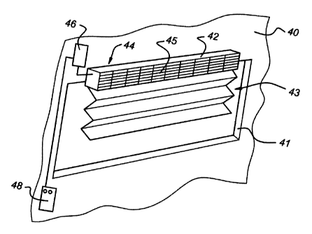
Fig. 1 shows a wall 40 having a window 41 along the upper end of which a head
rai142 of a pleated window covering 43 is niouirted. On the head rail a drive
assembly 44 is
mounted comprising an array of photovoltaic cells (solar cells) 45 facing
towards the
interior of the wall 40, an electric drive assembly 46 comprising a drive
motor, an
accumulator and a step-up converter connecting the accumulator to the solar
cells 45.
The assembly 46 can be completely integrated into the head rail 42 or can be
provided
as a separate unit attached to the wall 40. Control unit 48 for raising or
lowering the
window covering 43 is connected to the drive assembly 46.
Fig. 2 shows an alternative embodiment of a window covering comprising a
vertically deploying venetian blind, having horizontal slats 50 suspended from
a head
rail 42. Solar cells 45 are mounted on a windowsill and connected through
electrical
leads 51 to drive assembly 46. By operation of the control unit 48 the slats
50 may be


CA 02369306 2003-01-22

6
raised or lowered or may be changed in orientation by rotating around their
longitudinal
axes.
Fig. 3 schematically shows a drive asseinbly according to the present
invention,
comprising an electric motor 52 for raising or lowering the window covering
and/ or
changing the orientation of the slats 50, an electrical circuit 53, an
accumulator or
battery 54, a step-up converter 55 and a photovoltaic cell 45. The electrical
circuit 53
may comprise a step-up converter for increasing the voltage derived from the
battery
54. The battery 54 may comprise a metal hydride accumulator, an alkaline
manganese
battery, a lithium ion battery,, or a plurality of lithium ion batteries in
series.
In an embodiment, the accumulator has a capacity not exceeding 1.4 Ah. The
battery may be a 3.6 V battery systeni, whereas the electric motor 52 may
operate at 12
V DC at the power requirement not exceeding 50 mWh per day.
In a preferred embodiment the active operation of the electric motor 52 does
not
exceed 40 s per day.
Fig. 4 shows a step-up voltage converting unit 1 having a voltage converting
circuit, or low voltage converter stage 2, connected to a second converter
stage 3. The
low voltage converter stage 2 comprises an input terminal 4, an inductive
element 5,
first and second switches 6, 7 and a capacitive element such as capacitor 8.
Switches 6 and
7 are with a first terminal connected to the inductive elernenC 5 and with a
second terminal
to a reference voltage line 9. The second terminal of capacitive element 8 is
connected to
the output of a diode 11 and to the supply voltage terminal 12. The supply
voltage terminal
12 is connected to a power input 14 o f a first oscillator 13. A start-up
output 15 of the first
oscillator 13 is connected to the base or gate electrode 31 of switch 6
whereas the oscillator
output 16 is connected to the gate electrode 32 of switch 7. The supply
voltage an output
terminal 12 of low voltage converter stage 2 is connected to the second
terminal of
inductive element 28 and to a power input 22 of second oscillator 17 of
second. converter
stage 3. The oscillator output 18 connects to the gate electrode 33 of switch
19. A diode
20 and capacitor 21 are connected between the inductive element 28 and
reference voltage
line 23. Electrical device 24 is comiected across output terminals 25, 26 of
second converter
stage 3.
When at start-up a varying low voltage supply, such as a solar cell, is
connected
to input terminals 4 and 27 of' the voltage converting uriit 1, and switches
6, 7 are
closed, the capacitive element 8 is charged, creating a small voltage on the
output


~ CA 02369306 2003-01-22 ~

7
terminal 12 and on oscillator power input 14. The small power input into the
first oscillator
13, results in a pulse shaped signal on start-up output 15 at a low gate
control voltage
level V, , which may be a few tenths of Volts, periodically opening and
closing the
switch 6 at the frequency of for instance 100 k.Hz. This causes a periodic
current
through the switch 6 resulting in a rising current throug:h the inductive
element 5,
charging capacitor 8 that is rectified by diode 11 and results in an
increasing voltage at
the supply voltage termiiial 12 and consequently at the power input 14 of the
first oscillator 13.
This effect continues until the voltage level at supply terminal 12 reaches a
predetermined level, after which low voltage controlled switch 6 is de-
activated
(opened) and high voltage controlled switch 7 is operated from oscillator
output 16.
The second switch 7 is operated at a control voltage level V::Z until the
supply voltage at
supply voltage terminal 12 is for instance a few volts. The supply voltage is
input into
second converter stage 3 at the second terminal of inductive element 28 and
into power
input 22 of second oscillator 17. At oscillator output 18, a pulsed control
signal
operating the gate electrode 33 of switcll 19 is generated. By switching on
and off the
switch 19, the energy stored in inductive element 28 is transferred to
capacitor 21 until
a predetermined voltage level is reached. At this predeterrnined level, such
as voltage
levels between 1.5-12V, switch 19 is opened such that electrical energy is
stored in
inductive element 28, to be released again upon closing of the switch 19.
As the step-up voltage-converting unit l. generates its own supply voltage
from a
situation of rest, the step-up converter is self-starting.
Fig. 5 shows in detail the components of the voltage converter stage 2 and
second
converter stage 3 according to the present invention. The following letter
symbols
apply:
T, : low power, logic level MOSFET;

T 2 : switching MOSFET; power MOSFET;
Li : switching coil with high inductance;
L4 : switching coil;

D, , D 2 : rectifying diodes;

C 9, C z, , C, : smoothening electrically controllable capacitors (elco's);

U IA -U IF ; U,C : low voltage inverter gates manufactured by Philips
Electronics
under type number 74HC 14;


CA 02369306 2003-01-22 ~
8

T4 switching bipolar transistor;
D Z, D4 : Schottky diodes;

C 3 relatively small capacitor.

The second converter stage 3 operates according to known DC-DC' voltage
converter principles according to which the sniall fluctuating voltage V-solar
at the
input of coil 28 is stored in the coil when switching MOSFET 19 is opened.
Upon
closing of the switching MOSFET 19, the energy is released from the coil 28
and
supplied via rectifier diode 20 to smoothing capacitors 21 resulting in an
increased
voltage across output terminals 25, 26. In order to be self=starting, voltage
converter
circuit or step-up circuit 2 is provided wherein the oscillator 13 is
constructed of active
component of the type of Philips low voltage inverter ports or gates U1C, and
UIE. 'The inverter
ports can generate at their output, voltages at an input voltage of V cc of
below 0.4V at
start-up.

At low supply voltages V , transistor T3 is switched-off and a very low
alternating voltage is supplied via start-up output 15 of oscillator 13 to a
coupling
capacitor C Z and from thereon to the base 31 of transistor T, . Schottky
diode D 4 is
used as a positive clamp such that a small alternating voltage appears on the
base 31
with an offset of 0.4V. 'The solar cell voltage is about 0.4V. The transistor
T 4 will go in
conduction at a gate voltage of about 0.6V, such that the gate voltage need
only be 0.2

V in order to get transistor T4 into conduction. It has appeared that the
oscillating
inverter gate U,c of oscillator 13 can supply enough energy to get the
transistor T4 into
conduction. This causes a periodic current in the collector c of transistor T
4. Since the
transistor T 4 is coupled with a switching coil with a relatively high
inductance L, and
a relatively small capacitor C3, the periodic current in the collector c
results in an AC-

voltage across the coil 5. This AC-voltage is rectified through Schottky diode
D 2 and
appears on supply voltage terminal 12 and is fed back at the supply of low
voltage
inverter gates U,c -U,F . Each tirne V c, rises, the voltage level at the
start-up output 15
of the oscillator 13 rises, resulting in better control of switching
transistor T 4. Proper
gating of transistor T 4 results in more power being stored in coil 5,
increasing supply

terminal voltage V,, etc. At the outlet 30 of the oscillator L1,~. , a
coupling capacitor C 4


CA 02369306 2003-01-22

9
is provided which operates a low voltage inverter gate IJ ,L . The output of
the oscillator
U,E is connected to the control gate. 32 of a low power logic level of the
MOSFET T,.
The coupling capacitor C 4 ensures that the MOSFET of T, switches at the
beginning
or start-up in phase with transistor T, .

When the supply voltage V ,r rises above the treshold level of logic level
MOSFET T, , transistor T 3 goes into conduction, pulling the input of
oscillator U,c to
ground such that first transistor T a is switched-off and logic level MOSFET
T, takes
over. Now V,, can rise to for instance 3 V wherein the final power conversion
up to
voltages ranging from 1.5-12.0 V is effected by power MOSFET T Z of second

converter stage 3. When V,,reaches its desired end level, the varying supply
level V-
solar will place transistor T in conduction pulling the input of oscillator
U1F to ground
and de-activating switch T 2.

Fig. 6 shows another embodiment of a low voltage solar converter including a
step-up DC-DC converter (sometime also called: a voltage increasing chopper).
The
main components of the step-up converter are:

inductor/inductance L 4; semiconductor switch T,, and supplemental N-channel
MOSFET T 2; diode D 1(Schottky ZHCS 750) and capacitor/capacitance in the form
of
high capacity elco C 23 compensated for low resistance by additional
capacitors C19 and
C 20 . Semiconductor switch T 4 operates the step-up converter at those times
when the

voltage is too low to operate the MOSFE'T switch T. Switch T, is operated by
an
oscillator circuit as indicated in Fig. 3 by a dash-dotted box. 'I'he output
of the oscillator
connects to the start-up oscillator connector of the step-up converter where
Schottky
diode D 3(ZHCS 750) adds the output voltage of the solar panel 425a to the
pulsed
voltage generated by the oscillator. The resulting voltage is offered to the
base of T 4.

As soon as the voltage offered to the step-up converter is high enough for the
MOSFET
switch T2 to operate, the oscillator output is grounded tlirough semiconductor
T3 of
the oscillator circuit. Then the MOSFET T2 is controlled from the "N-gate"
output of
the central micro processor 471 and a further P-channel MOSFET TI is
controlled from
the "P-gate" output of the processor 471 to take over t-rom the Scliottky
diode D, I. The

P and N-gates of the processor 471 are software driven. In this manner a
particularly


CA 02369306 2003-01-22

advantageous step-up converter has been obtained. 'rhe alternative use of
semiconductor switches T4 and T2 provides for a register of compound step-up
converter that has optimal characteristics for each of a low voltage and a
higher voltage
range. The provision of Schottky diode D a enables to offer an as high as
possible

5 voltage to the base of the low voltage semiconductor switch T4. The
additional
MOSFET switch T,, which is positioned in parallel to diode D,, allows to
eliminate
the losses, which normally occur in diodes such as D, .

Fig. 7 shows the input and output voltages V, , V o of inverter ports U,C and
U,E
which are inverting Schmitt-trigger inverter ports. Generally, at a supply
voltage V,, of
10 1 V, the negative-going treshold V,., will be about 0.5V, the positive-
going treshold

V,.Z being several tenths of Volts higher. The output voltage V. will be
limited to a
maximum of supply voltage V, The inventors have found out that at supply
voltages
V,, below specification of the manufacturer, there is a region of the inverter
port below
V,., at which at low supply voltage V,,. there still is a hysterises in the
output signal

such that an oscillator can be obtained by feedback of the output signal to
the input
via resistor R Z. At a supply voltage of V , 0.4V the input at the inverter
gate U,c is
given in Fig. 8, at a level of about 300 mV, at a frequency of about 4 kHz.

In Fig. 9, the output at inverter gate U,c is given at a level of 400 mV with
a
frequency of about 20 kHz. Surprisingly, at low supply voltages V,, and at low
input
levels below the negative-going treshold V,, according to specifications, it
is still

possible to obtain an oscillator using inverter gate U,t. such that start-up
of the step-up
converter can be obtained by use of said component.

Representative Drawing
A single figure which represents the drawing illustrating the invention.
Administrative Status

For a clearer understanding of the status of the application/patent presented on this page, the site Disclaimer , as well as the definitions for Patent , Administrative Status , Maintenance Fee  and Payment History  should be consulted.

Administrative Status

Title Date
Forecasted Issue Date 2009-03-10
(22) Filed 2002-01-30
(41) Open to Public Inspection 2002-07-30
Examination Requested 2007-01-23
(45) Issued 2009-03-10
Deemed Expired 2012-01-30

Abandonment History

There is no abandonment history.

Payment History

Fee Type Anniversary Year Due Date Amount Paid Paid Date
Application Fee $300.00 2002-01-30
Registration of a document - section 124 $100.00 2002-05-27
Maintenance Fee - Application - New Act 2 2004-01-30 $100.00 2003-12-16
Maintenance Fee - Application - New Act 3 2005-01-31 $100.00 2004-12-13
Maintenance Fee - Application - New Act 4 2006-01-30 $100.00 2005-12-12
Maintenance Fee - Application - New Act 5 2007-01-30 $200.00 2006-12-08
Request for Examination $800.00 2007-01-23
Maintenance Fee - Application - New Act 6 2008-01-30 $200.00 2007-12-17
Final Fee $300.00 2008-11-25
Maintenance Fee - Application - New Act 7 2009-01-30 $200.00 2008-12-16
Maintenance Fee - Patent - New Act 8 2010-02-01 $200.00 2009-12-16
Owners on Record

Note: Records showing the ownership history in alphabetical order.

Current Owners on Record
TURNILS AB
Past Owners on Record
OSINGA, ANNE J.
WELVAADT, JOCHEM
Past Owners that do not appear in the "Owners on Record" listing will appear in other documentation within the application.
Documents

To view selected files, please enter reCAPTCHA code :


To view images, click a link in the Document Description column. To download the documents, select one or more checkboxes in the first column and then click the "Download Selected in PDF format (Zip Archive)" or the "Download Selected as Single PDF" button.

List of published and non-published patent-specific documents on the CPD .

If you have any difficulty accessing content, you can call the Client Service Centre at 1-866-997-1936 or send them an e-mail at CIPO Client Service Centre.


Document
Description 
Date
(yyyy-mm-dd) 
Number of pages   Size of Image (KB) 
Drawings 2002-01-30 6 356
Abstract 2002-01-30 1 42
Representative Drawing 2002-05-02 1 13
Description 2002-01-30 10 610
Cover Page 2002-07-26 1 53
Description 2002-03-12 10 542
Claims 2002-01-30 3 121
Abstract 2002-03-12 1 36
Claims 2002-03-12 3 97
Drawings 2002-03-12 6 146
Description 2003-01-22 10 604
Drawings 2003-01-22 6 154
Claims 2007-02-20 14 686
Cover Page 2009-02-16 2 64
Representative Drawing 2009-02-16 1 17
Correspondence 2002-02-26 1 35
Assignment 2002-01-30 2 80
Correspondence 2002-03-12 21 851
Assignment 2002-05-27 4 161
Prosecution-Amendment 2003-01-22 13 605
Prosecution-Amendment 2007-01-23 1 42
Prosecution-Amendment 2007-02-20 16 727
Correspondence 2008-11-25 2 48