Note: Descriptions are shown in the official language in which they were submitted.
CA 02369434 2002-01-25
1
CRYSTAL OSCILLATOR AND A SIGNAL OSCILLATION METHOD
THEREOF
Background of the Invention
Field of the Invention
The present invention relates to a crystal
oscillator, and more particularly, to a crystal
oscillator preventing abnormal oscillation by which an
oscillation frequency suddenly (discontinuously)
changes due to a temperature change.
Description of the Related Art
A crystal oscillator is used as a frequency and
time reference source in various types of electronic
devices such as a digital control device, a
communications device, etc. Among communication
devices where a crystal oscillator is used, a
communications device that is normally installed
outdoors and demanded to be used under an environment
of a severe temperature change, for example, like a
broadband wireless communications device which secures
a large amount of a communications line.
Figs. 1 and 2 exemplify a general crystal
oscillator. Fig. 1 is a circuit: diagram showing the
crystal oscillator,.whereas Fig. 2 is a cross-sectional
CA 02369434 2002-01-25
2
view of the structure of the crystal oscillator.
The crystal oscillator is mainly composed of a
crystal vibrator 1 and an oscillation circuit unit 2,
and forms, for example, an oscillation circuit 3 of a
Colpitts type. The crystal vibrator 1 has a
configuration where an electrode (not shown) is formed,
for example, in an AT-cut quartz crystal element, and
the quartz crystal element is held and hermetically
sealed in a metal box 5 from which a lead 4 is extended.
The oscillation circuit uriit 2 is composed of a
capacitor that forms a resonance circuit along with the
crystal vibrator 1 (inductor component), an amplifier
for oscillation, etc. Normally, an oscillation
amplifying stage 6 amplifying the oscillation output
from the oscillation circuit unit 2 is connected to the
oscillation circuit unit 2. The crystal vibrator 1 and
other elements 7, which form the crystal oscillator,
are arranged on a circuit board 9 having a lead 8, and
sealed by a cover not shown.
With such a crystal oscillator, the oscillation
frequency of an output signal changes with temperature
mainly due to the frequency-temperature characteristic
of the crystal vibrator 1.
If the quartz crystal element of the crystal
vibrator 1 is AT-cut, the frequency-temperature
CA 02369434 2002-01-25
3
characteristic of an oscillation frequency becomes a
tertiary curve whose inflection point is close to an
ordinary temperature (25 C) . Normally, as shown in Fig.
3, a crystal vibrator is selected so that the
frequency-temperature characteristic that has a
maximum value in a low-temperature area equal to or lower
than an ordinary temperature, and a minimum value in
a high-temperature area higher than the ordinary
temperature is implemented. Namely, the crystal
vibrator (the cutting angle of the AT cutting) is
selected to have such a frequency-temperature
characteristic, whereby an oscillation frequency
change due to a temperature change is suppressed within
a monotonously changing range between the maximum and
the minimum values in a wide temperature range having
the ordinary temperature as a center. Note that the
temperature points of the maximum and the minimum values
depend on the cutting angle of the AT cutting.
However, the crystal oscillator having the above
described configuration has a problem of causing
abnormal oscillation in a low-temperature area of 0 C
or lower. The abnormal oscillation referred to here
means not a phenomenon that an oscillation frequency
moderately changes according to the
frequency-temperature characteristic, but a phenomenon
CA 02369434 2002-01-25
4
that the oscillation frequency discontinuously changes,
and is commonly called a jump (micro-jump) of an
oscillation frequency.
Fig. 4 shows such a jump (micro-jump) in the
frequency-temperature characteristic of the crystal
vibrator.
The frequency-temperature characteristic has an
extremely small resonance point at a certain temperature
point equal to or lower than 0 C due to some reason
or coincidence of a plurality of conditions, so that
an oscillation frequency suddenly changes, for example,
as shown in Fig. 4. This is also called a micro-jump,
and is not found when the frequency-temperature
characteristic is measured in a manufacturing process.
For this reason, there is a problem that abnormal
oscillation in a low-temperature area cannot be avoided
under an environment of 0 C or lower. Note that, however,
the micro-jump does not occur in all of crystal
oscillators.
The above provided example refers to a mere
crystal oscillator. However, abnormal oscillation
occurs similarly, for example, in a crystal oscillator
having a configuration where a compensation voltage is
applied by inserting a voltage variable capacity element,
which is not shown, in an oscillation closed loop of
CA 02369434 2008-04-22
28151-99
the crystal oscillator, or in a crystal oscillator of,
what is called, a temperature compensation type, which
compensates for and flattens the frequency-temperature
characteristic by inserting a temperature compensation
5 circuit composed of a parallel circuit of a thermistor
and a capacitor in an oscillation closed loop.
Namely, even in these crystal oscillators, the
crystal vibrator 1 itself depends on an ambient
temperature, and exhibits the frequency-temperature
characteristic having a resonance point in a
low-temperature area. Therefore, a sudden change cannot
be avoided although temperature compensation is made,
and abnormal oscillation occurs. As a factor of causing
a micro-jump, there are various theories such as a result
of a phenomenon that condensation occurs at a
temperature equal to or lower than 0 C on the surface
of a quartz crystal element within a sealed box, and
the like. However, its details are not elucidated at
the present moment.
Summary of the Invention
Some embodiments of the present invention aim at
providing a crystal oscillator preventing abnormal
oscillation in a low-temperature area.
CA 02369434 2008-04-22
28151-99
6
A crystal oscillator according to an aspect of the
present invention comprises an oscillation unit and a heat
source unit.
The oscillation unit is composed of a crystal
vibrator having a frequency-temperature characteristic
with which a resonance frequency changes according to
a temperature, and an oscillation circuit unit.
The heat source unit, which abuts against the
crystal vibrator, keeps the temperature of the crystal
vibrator higher than a temperature at which the crystal
vibrator causes abnormal oscillation.
A crystal oscillator having another configuration
comprises an oscillation unit having a crystal vibrator, and
a heat source unit keeping the temperature of the crystal
vibrator higher than a temperature where the crystal
vibrator causes abnormal oscillation.
This abnormal oscillation is caused, for example,
by a micro-jump that occurs in the crystal vibrator.
The crystal vibrator is kept, for example, at a
temperature higher than 0 C.
The heat source unit in either of these crystal
oscillators may be configured, for example, by a power
transistor that amplifies an oscillation output.
CA 02369434 2008-04-22
28151-99
7
According to some embodiments of the present
invention, the crystal vibrator is kept by the heat source
unit at a temperature higher than a particular temperature,
so that abnormal oscillation does not occur even in a
low-temperature area.
There is also provided a crystal oscillator,
comprising: oscillation means having a crystal vibrator; and
heat source means for keeping a temperature of the crystal
vibrator higher than a temperature where the crystal
vibrator causes abnormal oscillation, wherein said heat
source means is configured by a power transistor which
amplifies an oscillation output.
Another aspect of the invention provides a signal
oscillation method preventing abnormal oscillation of an
oscillator having a crystal vibrator, comprising: keeping a
temperature of the crystal vibrator higher than a
temperature where the crystal vibrator causes abnormal
oscillation, using a heat source unit configured by a power
transistor which amplifies an oscillation output; and
outputting a signal in a state where the temperature is
kept.
Brief Description of the Drawings
Fig. 1 is a circuit diagram showing a general
crystal oscillator;
Fig. 2 is a cross-sectional view of the general
crystal oscillator;
Fig. 3 shows the frequency-temperature
characteristic of a general crystal vibrator;
CA 02369434 2008-04-22
28151-99
7a
Fig. 4 shows the frequency-temperature
characteristic of a crystal vibrator in order to explain a
micro-jump;
Fig. 5 is a cross-sectional view of a crystal
oscillator according to one embodiment;
Fig. 6 is a cross-sectional view of a crystal
oscillator in the case where a crystal vibrator for surface
mounting is used; and
Fig. 7 is a circuit diagram of a control circuit
having a configuration where the amount of heat is changed
according to a temperature.
Description of the Preferred Embodiment
First of all, the fundamental principle of the
CA 02369434 2008-04-22
28151-99
8
present invention is described.
According to the present invention, attention is
focused on a point that the above described micro-jump
problem does not occur if a crystal vibrator is kept
at a temperature higher than a temperature point (0 C
or lower), where abnormal oscillation occurs, in a
low-temperature area equal to or lower than the ordinary
temperature, and the crystal vibrator is made to abut
against a heat source, for example, a power transistor,
like a thermostatic oven used in a crystal oscillator
of a thermostatic oven disclosed by Japanese Patent
Publication NO. 1-195706, published on August 7, 1989, or the like.
As a result, the crystal vibrator is kept at a
temperature higher than a temperature (a temperature
point in a low-temperature area equal to or lower than
the ordinary temperature, for example, a temperature
point of 0 C or lower) where abnormal oscillation is
caused. Accordingly, even if the ambient temperature
becomes a temperature in the low-temperature area where
abnormal oscillation is caused, the crystal oscillator
does not become the temperature where the abnormal
oscillation occurs.
A crystal oscillator according to one preferred
embodiment of the present invention is described below.
A crystal oscillator according to this preferred
CA 02369434 2002-01-25
9
embodiment comprises a crystal vibrator 1 where an
AT-cut quartz crystal element is hermetically sealed
within a metal box 5 having a lead 4, an oscillation
circuit unit 2 having a capacitor and an amplifier for
oscillation, and an oscillation amplifying stage 6,
similar to the crystal oscillator represented by the
block diagram of Fig. 1. The crystal vibrator 1 and other
elements 7, which configure the crystal oscillator, are
arranged on a circuit board 9.
If voltage is applied to an oscillation circuit
3, the crystal vibrator 1 is excited, an output signal
of a particular frequency determined by the shape of
the quartz crystal element of the.crystal vibrator 1
is output from the oscillation circuit 3, and the signal
is amplified and output by the oscillation amplifying
stage 6.
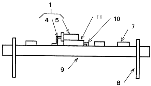
Fig. 5 is a cross-sectional view of the crystal
oscillator according to this preferred embodiment. In
this figure, the same constituent elements as those of
the crystal oscillator represented by the
cross-sectional view of Fig. 2 are denoted with the same
reference numerals, and detailed explanation about
these elements are omitted in the explanation provided
below.
In the crystal oscillator shown in Fig. 5, a power
CA 02369434 2002-01-25
transistor 11 having a lead 10 independent from an
oscillation circuit is arranged on a circuit board 9.
Additionally, the crystal oscillator 1 is placed so that
it abuts against the power transistor 11. Here, the main
5 surface of the crystal vibrator 1(a metal box 5) is
made to face and abut against the power transistor 11,
and a lead 4 is bent to connect to a wiring pattern (not
shown) of the circuit board 9.
With such a configuration, the crystalvibrator
10 1 is kept at least at a temperature higher than 0 C
by the heat generated by the power transistor 11.
Accordingly, even if an ambient temperature changes to
a temperature in the low-temperature area, for example,
0 C or lower, the crystal vibrator is kept at a
temperature higher than 0 C. Consequently, the crystal
oscillator can supply a stable oscillation frequency
without causing abnormal oscillation which arises at
a temperature point of 0 C or lower.
In Fig. 5, a crystal vibrator having a
configuration where the quartz crystal element is
hermetically sealed within the metal box 5 having the
lead 4 is adopted as the crystal vibrator 1. However,
the present invention is also applicable, for example,
to a crystal vibrator for surface mounting, in which
a quartz crystal element is hermetically sealed within
CA 02369434 2002-01-25
11
a ceramic box having a mounting electrode on its rear
side.
Fig. 6 is a cross-sectional view of the crystal
oscillator in this case.
In this figure, a crystal vibrator 12 for surface
mounting is mounted on a circuit board 9, and a power
transistor 11 is placed on the crystal vibrator 12 so
that the heat is conveyed to the crystal vibrator 12.
The power transistor 11 that is used as a heat
source may be newly arranged only for the use purpose
of a heat source. Or, a transistor used for another
purpose, such as a power transistor for amplifyingan
oscillation output, a power transistor of a power supply
or a regulator may be available. Or, heat generated by
a collector (source) loss of a transistor of a
transmitter may be available as a heat source.
Additionally, the temperature of the crystal
vibrator is assumed to be kept higher than 0 C. However,
for example, if a temperature in a low-temperature area,
at which the crystal vibrator causes abnormal
oscillation, is clear, the crystal vibrator may be kept
at a temperature higher than that temperature.
Furthermore, the above described preferred
embodiment adopts the power transistor 11 as a heat
source which makes the crystal vibrator warm. However,
CA 02369434 2002-01-25
12
other elements may be available asa heat source only
if the temperature of the crystal vibrator can be kept
higher than a temperature point where abnormal
oscillation is caused. For example, a ceramic heater,
a crystal vibrator around which a nichrome wire is wound
may be available.
Still further, in the above described preferred
embodiment, the crystal vibrator is merely placed on
the heat source. However, the amount of heat generated
by this heat source may be varied according to a
temperature.
Fig. 7 exemplifies an implementation of the
configuration where the amount of heat is varied
according to a temperature. In the configuration example
shown in this figure, an electric current that is
supplied to a heat source is controlled by a
thermo-sensitive element (such as a posistor or a
thermistor), so that the amount of heat is increased
at a low temperature.
In the configuration shown in this figure, a power
transistor 15, which becomes a heat source, is
emitter-grounded, and a load resistor 14 and bias
resistors 13a and 13b are respectively arranged on
collector and base sides. The resistor 13b on the
grounded side among the two base bias resistors 13a and
CA 02369434 2002-01-25
13
13b is assumed as a thermistor whose resistance value
decreases with an increase in the temperature.
With such a configuration, the resistance value
of the resistor 13b decreases as the temperature rises.
As a result, the bias voltage of the power transistor
drops, so that the current between the emitter and
the collector decreases, and the amount of heat
generated by the power transistor 15 becomes small.
Inversely, the bias voltage rises as the temperature
10 drops. Therefore, the current between the emitter and
the collector increases, and the amount of heat
generated by the power transistor 15 becomes large.
The configuration of this preferred embodiment
differs from an existing crystal oscillator using a
15 thermostatic oven. Namely, with the existing crystal
oscillator having a thermostatic oven, a crystal
vibrator must be kept at a constant temperature, for
example, a temperature which becomes a minimum value
on a high temperature side. Therefore, a control circuit
for this implementation becomes strict (complex).
However, with the crystal oscillator according to this
preferred embodiment, it is sufficient to only keep a
crystal vibrator at a temperature higher than a
predetermined temperature. Therefore, its control
circuit becomes extremely simple. Accordingly, the
CA 02369434 2002-01-25
14
existing crystal oscillator and the crystal oscillator
according to the present invention definitely differ.
Furthermore, the above provided explanation takes
a mere crystal oscillator as an example. However, the
present invention is applicable also to the above
described crystal oscillator having a configuration
where a compensation voltage is applied by inserting
a voltage variable capacity element in an oscillation
closed loop of the crystal oscillator, and to the
temperature compensation oscillator that comprises a
temperature compensation circuit and flattens a
frequency-temperature characteristic. The temperature
compensation oscillator may be configured so that a
thermo-sensitive element of the temperature
compensation circuit is arranged close to a heat source,
and the temperature of a crystal vibrator is.detected
by the thermo-sensitive element and compensated.