Note: Descriptions are shown in the official language in which they were submitted.
CA 02369673 2004-10-06
64881-496
SPECIFICATION
A METHOD FOR FABRICATING AN OPTICAL WAVEGUIDE DEVICE
(Technical field)
This invention relates to an optical waveguide device and its
fabrication method applicable for long haul and large capacity optical fiber
communication system and an optical measuring instrument, particularly to an
optical waveguide device having a metal-cladding type optical polarizer and
its
fabrication method for achieving a high extinction ratio and stabilizing the
device
performance against fluctuation of incident lightwave.
(Background Art)
An optical waveguide device comprising an optical waveguide, a
buffer layer and electrodes which are fabricated on a substrate having electro-
optic effect, such as lithium niobate (LN), has been widely employed for long
haul and large capacity optical fiber communication system and an optical
measuring instrument.
The optical waveguide device is fabricated as follows: First of all,
the optical waveguide is formed on the LN substrate by a Ti thermal diffusion
method, and the buffer layer made of Si02, and the electrodes for modulation
of
lightwave propagating through the optical waveguide, are successively
fabricated
on the substrate. Then, the substrate is diced into chips and they are mounted
on cases. Finally, optical fibers are connected to both ends of each chips to
complete optical waveguide devices.
In general, the optical waveguide devices are operated using the
lightwave with perpendicularly or horizontally polarized to a main surface of
a
substrate. From this point of view, a polarization maintaining fiber is
usually
connected to the input of the optical waveguide of the device, and the
linearly
polarized lightwave is introduced into the optical waveguide device.
However, if the polarization maintaining fiber is stressed from the
outside or non-linearly polarized lightwave is introduced, extinction ratio of
the
optical waveguide device would be degraded. As the result, the optical
waveguide device can not do on/off switching of lightwave correctly, so that
the
S/N ratio is degraded in the signal transmittance.
CA 02369673 2004-10-06
64881-496
To solve the above-mentioned problem, a metal-cladding type optical
polarizes proposed by Suematsu et al. in ''Appl. Phys. Lett., Vol. 21, No. 6
(1972)" is applicable for the optional waveguide device. The metal-cladding
type optical polarizes is utilizing difference in degree of electric field
absorption
depending on the state of polarization. Concretely, by the metal-cladding type
optical polarizes, only polarized lightwave horizontal to a main surface of a
substrate (TE mode lightwave) is transmitted, and a polarized lightwave
perpendicular to the main surface (TM mode lightwave) is absorbed. The above
optical waveguide device can exhibit a relatively high extinction ratio,
regardless
of its simple structure.
For the reduction of the excess absorption of the TE mode lightwave
and the achievement of high extinction ratio, a dielectric film having a lower
refractive index than that of the core of the optical waveguide may be
fabricated
as an intermediate layer between the optical waveguide and the metal-cladding
type optical polarizes.
On the other hand, for the improvement of velocity matching, a buffer
layer made of a dielectric material, such as Si02, is fabricated between the
substrate and the electrodes to modulate the lightwave propagating through the
optical waveguide. In this case, it is proposed that the buffer layer is
partially
etched by reactive ion etching using a fluorine-based gas such as CF4 or CHF3
to
form an opening so as to expose the part of the substrate, and the metal-
cladding
type optical polarizes is provided in the opening. Therefore, the metal-
cladding
type optical polarizes can be integrated on the optical waveguide device
having a
thick buffer layer.
However, in this case, the buffer layer may be over-etched due to the
fluctuation in its thickness and/or in the etching rate corresponding to
different
etching batches, so that the substrate may be partially etched. Therefore, if
the
metal-cladding type optical polarizes is provided on the etched substrate in
the
opening, the polarization property of the metal-cladding type optical
polarizes may
be fluctuated according to degree of over-etching against the substrate,
resulting
in the deterioration of the extinction ratio of the optical waveguide device.
On the other hand, the metal-cladding type optical polarizes may be
fabricated on the intermediate layer composing by dielectric materials. In
this
-2-
CA 02369673 2004-10-06
64881-496
case, during the long-term use of the optical waveguide device, mechanical
peeling of the metal-cladding type optical polarizes due to heat cycle and/or
thermal shock can be avoided.
However, when the metal-cladding type optical polarizes is fabricated
on the intermediate layer composing by oxides, such as Si02, it is oxidized
and
corroded by long-term use. As a result, the performance of the optical
waveguide device as having the metal-cladding type optical polarizes can not
be
stabilized for a long time.
(Description of the invention)
It is an object of the present invention to provide an fabrication
method to be able to realize a high extinction ratio for a long time through
the
performance of the metal-cladding type optical polarizes, irrespective of its
configuration being formed on an intermediate layer or in an opening at the
buffer layer, with keeping its formation advantages.
For achieving the above object, this invention relates to an optical
waveguide device comprising:
a substrate made of a material with an electro-optic effect,
an optical waveguide formed on the substrate to transmit a lightwave,
a modulation electrode to modulate the lightwave,
a metal-cladding type optical polarizes to remove the unnecessary polarized
component of the lightwave, and
an intermediate layer, between the substrate and the metal-cladding type
optical polarizes, made of at least one dielectric material selected from the
group
consisting ofAOx, BZOy, COz (A:divalent element, Barivalent element,
C:quadrivalent element, 0<x<1, 0<y<3, 0<z<2, O:oxygen).
The inventors have intensely studied to stabilize the performance of
an optical waveguide device having a metal-cladding type optical polarizes,
and
then, investigated the structure of the optical waveguide device in detail.
As a result, they found that the metal-cladding type optical polarizes
was not peeled if it was fabricated on an intermediate layer with low internal
stress, as mentioned above.
Since the metal-cladding type optical polarizes is required to be
formed on the optical waveguide, the intermediate layer must be formed on the
-3-
CA 02369673 2004-10-06
64881-496
same optical waveguide. Therefore, if the intermediate layer is made of a
material with higher refractive index than that of the substrate or the
optical
waveguide, a lightwave propagating through the optical waveguide is leaked
toward the intermediate layer. Thus, the intermediate layer is required to be
made of a material with relatively lower refractive index such as dielectric
oxides.
As mentioned above, however, if the metal-cladding type optical
polarizer is provided on the intermediate layer composing by dielectric
oxides, it
is oxidized and corroded. Therefore, the inventors have precisely studied to
clarify the mechanism of the oxidization and corrosion. As a result, they have
found that the excess oxygen in the intermediate layer was extricated with
time,
and diffused into the metal-cladding type optical polarizer formed on the
intermediate layer, thereby to oxidize and corrode the polarizer.
Based on the above-mentioned study, the inventors have made a
investigation to inhibit the extrication of the excess oxygen. As a result,
they
have found that oxidization and corrosion of the metal-cladding type optical
polarizer could be inhibited when the intermediate layer was made of a
dielectric
oxides having a lower oxygen concentration than that of its stoichiometric
concentration, because the excess oxygen was not generated in the intermediate
layer.
This invention is achieved by the extensive and detailed researches as
mentioned above.
The optical waveguide device of the present invention is created
directly from the above researches, and has the intermediate layer of
dielectric
oxide between the substrate and the metal-cladding type optical polarizer.
According to the present invention, mechanical peeling, oxidization
and corrosion of the metal-cladding type optical polarizer can be avoided, and
thus, the performance of the optical waveguide device can be stabilized for a
long time.
Furthermore, this invention relates to a fabrication method of an
optical waveguide device consisting of an optical waveguide, a buffer layer, a
metal-cladding type optical polarizer and a modulation electrode on a
substrate
with an electro-optic effect, comprising:
a first step to form the optical waveguide on the substrate,
-4-
CA 02369673 2004-10-06
64881-496
a second step to fabricate the buffer layer on the substrate,
a third step, by means of partial removal of the buffer layer employing non-
reactive dry-etching, to form a first opening so that the corresponding part
of the
main surface of the substrate on which the optical waveguide is formed, is
partially or entirely exposed, and
a fourth step to fabricate the metal-cladding type optical polarizes on the
substrate inside the first opening.
Also, the inventors investigated, for a LN substrate, the cause of
fluctuation in optical performance of the metal-cladding type optical
polarizes,
when it was fabricated in a buffer layer opening of which the substrate was
slightly etched in the formation process.
As the result, they found that the metal-cladding type optional
polarizes was corroded when it was fabricated in such opening, although it was
not corroded when it was fabricated directly on the substrate without forming
buffer layer. As they made further investigation on the corrosion phenomenon,
they found that the excess oxygen from the main surface of the substrate was
the
cause of its corrosion.
Then, since the excess oxygen is generated when the substrate is
attacked by fluorine-based gas plasma because of over-etching of the buffer
layer,
the inventors conceive the following mechanism of generating the excess
oxygen.
That is, when the chemically reactive etching using fluorine-based gas plasma
is
employed, the fluorine radicals as main etching species are selectively
reacted
with the lithium constituting the LN substrate, to form fluorides. Because,
the
lithium is selectively extricated from the LN substrate as lithium fluoride,
the
excess oxygen is generated.
On the above excess oxygen generating mechanism, the inventors
employ non-reactive physical etching using argon gas plasma, and the buffer
layer is partially etched to form an opening, in which the metal-cladding type
optical polarizes is fabricated. In this case, the metal-cladding type optical
polarizes is never corroded, and thus, the optical performance of the
polarizes is
not changed.
This invention is also achieved through the vast research and
development.
-5-
CA 02369673 2004-10-06
64881-496
According to the present invention, even though the substrate is
attacked by fluorine-based gas plasma because of over-etching of the buffer
layer
occurred in the fabrication process of buffer layer opening, the excess oxygen
is
not generated on the main surface, particularly in the superficial layer of
the
substrate. Therefore, when the metal-cladding type optical polarizer is
fabricated in the opening, it is not oxidized and corroded.
Accordingly, the polarization property of the metal-cladding type
optical polarizer can be stabilized and thus, the optical waveguide device
having
a high extinction ratio can be provided.
(Brief description of drawings)
The invention will be more particularly, described with reference to
the accompanying drawings, in which:
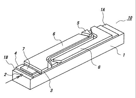
Fig. 1 is a perspective view showing an optical waveguide device
according to the present invention,
Fig. 2 is a perspective view showing an optical waveguide device
according to the fabrication method of the present invention, and
Fig. 3 shows DC drift curves of optical waveguide devices according
to the present invention and the referential example.
(Best mode for carrying out the invention)
The invention will be described in detail with reference to the above
drawings as follows:
Fig. 1 is a perspective view showing an optical waveguide device
according to the present invention. Herein, for the clarity of the features of
the
present invention, detail parts of the optical waveguide device are not shown
in
the drawing.
The optical waveguide device 10 depicted in Fig. 1 has a substrate 1
made of a material with an electro-optic effect and a Mach-Zehnder type
optical
waveguide 2 fabricated on the substrate 1. And, a buffer layer 3 is formed in
on
main surface 1 A of the substrate 1. Moreover, an intermediate layer made of
at
least one dielectric material selected from the group consisting of AOx, B20y,
COz (A:divalent element, Barivalent element, C:quadrivalent element, 0<x<l,
0<y<3, 0<z<2, O:oxygen) is fabricated at the edge portion 1 B of the main
surface
lA of the substrate 1.
-6-
CA 02369673 2004-10-06
64881-496
A signal electrode 5 and ground electrode 6, constituting of a
modulation electrode for the optical waveguide 2, are provided on the buffer
layer 3. Then, a metal-cladding type optical polarizes is fabricated on the
corresponding part of the intermediate layer 4 below which the optical
waveguide is provided.
In the optical waveguide device 10 depicted in Fig. 1, an incident
lightwave introduced in the arrow direction, is polarized by the metal-
cladding
type optical polarizes 7, and then, the lightwave component parallel to the
main
surface lA of the substrate 1 (TE made lightwave) is selected by the metal-
cladding type optical polarizes 7. Therefore, only the parallel component is
transmitted through the optical waveguide 2, and modulated by a microwave
applied from the signal electrode 5 and the ground electrode 6. According to
the degree of phase shift in Mach-Zehnder interferometer the parallel
component
is extinguished or not distinguished and thus, the incident lightwave
(parallel
component) is switched to the state "on" or "off'.
As mentioned above, the metal-cladding type optical polarizes 7 is
provided on the intermediate layer 4 made of the above dielectric material in
the
optical waveguide device 10 depicted in Fig. 1. Therefore, the stress
generated
between the substrate 1 and the metal-cladding type optical polarizes 7 is
damped
at the intermediate layer 4, and thus, the mechanical peeling of the metal-
cladding type optical polarizes with time can be prevented. Moreover, the
excess oxygen is not generated in the intermediate layer 4, and thus, the
oxidization and the corrosion of the metal-cladding type optical polarizes 7
with
time can be prevented. Accordingly, the stable operation of the optical
waveguide device 10 having the metal-cladding type optical polarizes 7 can be
maintained for a long time.
It is required that the intermediate layer 4 is made of the above
dielectric material. Concretely, MgOx can be exemplified as the AOx. A120y,
Y20y can be exemplified as the B20y. Then, SiOz, ZrOz, HfOz and GeOz can
be exemplified as the COz.
Particularly, SiOz can be preferably used because it is not expensive
and easy to be formed as a thin film.
The metal-cladding type optical polarizes 7 is consisted of a metallic
CA 02369673 2004-10-06
64881-496
material, such as A1, Ag, Cr or Pt.
The thickness of the intermediate layer is determined on the refractive
index thereof. For example, the thickness of the SiOz intermediate layer is
preferably set within 50-100th. In this case, the object of the present
invention
can be realized effectively and efficiently. The thickness of the metal-
cladding
type optical polarizes 7 is generally set within 1000-3000A.
In the optical waveguide device 10 according to the present invention,
the signal electrode and the ground electrode may be made of a good conductive
metallic material such as Au, Ag or Cu.
The substrate I is required to be made of a material having an electro-
optic effect, for example, lithium niobate (LiNb03), lithium tantalate
(LiTa03)
and lead lanthanum zirconate titanate (PLZT). Particularly, the LiNb03 is
preferably used because the high quality crystal of it is inexpensively
available
and it is easy to form the optical waveguide by a Ti thermal diffusion method
and
so on.
The optical waveguide 2 can be fabricated by a conventional method
such as the Ti thermal diffusion method or a proton-exchanging method.
The intermediate layer 4 can be made by a conventional film-forming
method such as vacuum deposition method or a sputtering method.
In the case of using the sputtering method, the intermediate layer
made of the above-mentioned dielectric material can be deposited when only Ar
gas is introduced into a sputtering chamber.
Next, the fabrication method for an optical waveguide device
according to the present invention will be described, with reference to Fig.
2.
An optical waveguide device 20 depicted in Fig. 2 as a preferred
embodiment of the present invention has a substrate 1 I having an electro-
optic
effect, an optical waveguide 12 fabricated on the substrate 11, a signal
electrode
15 and a ground electrode 16 which constitute a modulation electrode. And, a
buffer layer 13 is provided between the substrate 11 and the signal and the
ground electrode 15 and 16. Moreover, a metal-cladding type optical polarizes
14 is fabricated on the left edge of the substrate 11 so that it is directly
contacted
to the main surface 11A of the substrate 11. In addition, DC electrode 17 is
fabricated on the right edge of the substrate 11 so that it is directly
contacted to
_g_
CA 02369673 2004-10-06
64881-496
the main surface 11 A of the substrate 11.
The DC electrode 17 applies a bias voltage to the optical waveguide
12 for controlling the operation point of the optical waveguide device 20.
A lightwave is introduced into the optical waveguide 12 of the optical
waveguide device 20 along the depicted arrow direction, and then, the
lightwave
component parallel to the main surface 11 A of the substrate 11 (TE made
lightwave) is selected by the metal-cladding type optical polarizer 14.
The parallel component is modulated by a microwave applied from the signal
electrode 15 and the ground electrode 16, and then, extinguished or not
extinguished. Accordingly, the incident lightwave (parallel component) is
switched to the state "on" or "off', corresponding to the non-extinction or
the
extinction of the incident lightwave.
In the present invention, first of all, the optical waveguide 12 is
fabricated on the electro-optic substrate 11 by a Ti thermal diffusion method,
a
proton-exchanging method, an epitaxial growth method and an ion implantation
method.
Subsequently, the buffer layer 13 is formed on the substrate 11 by a
well known film-forming method such as vacuum deposition method, a
sputtering method, an ion-plating method or a CVD method, depending on the
kind of the material to form the buf~'er layer 13.
The thickness of the buffer layer 13 is preferably set within 0.2-
2.0 pm, for velocity-matching between a lightwave propagating through the
optical waveguide 12 and a microwave as the modulating signal traveling along
the signal electrode 15 and the ground electrode 16, and for preventing the
absorption loss of the lightwave to the electrodes 15 and 16.
Then, in this invention, the buffer layer 13 is partially removed by
non-reactive dry-etching to form a first opening 18.
The non-reactive dry-etching process will be performed as follows:
First of all, a chromium mask is fabricated on the buffer layer 13 by a
vacuum deposition method so that the thickness of the chromium mask becomes
thicker than that of the buffer layer 13, e.g., 0.3-2.1 p.m. Then, a
photoresist is
spin-coated in a thickness of 0.7-1.0 pm on the chromium mask, and thereafter,
is
patterned by phototlithography. The corresponding part of chromium mask for
-9-
CA 02369673 2004-10-06
64881-496
the first opening 18 to be formed is removed by chemical etching. Then, the
residual photoresist is removed by an organic solvent.
Thereafter, the masked substrate is set in a dry-etching apparatus with
a high-density plasma resource like ECR, and the buffer layer 13 is dry-
etched.
In this case, only the corresponding part of the buffer layer 13 without the
chromium mask for the first opening 18 to be formed is etched and removed,
thereby to form the first opening 18. The residual chromium mask is removed
by chemical etching, etc.
In the above non-reactive dry-etching process, any kind of etching gas
to generate non-reactive plasma ion species can be employed. Particularly,
inert
gas can be preferably employed because it has a relatively high etching rate
and
is chemically stable to be handled easily. Especially, argon gas is preferably
employed because it is inexpensively available and the etching rate can be
easily
controlled.
In the case that a relatively thick buffer layer up to 1.0 p,m or over is
formed, it is desired that reactive dry-etching is employed together with the
non-
reactive dry-etching to form the first opening 18.
That is, first of all, the buffer layer 13 is etched by the reactive dry-
etching. Then, just before the main surface 11A of the substrate 11 is
exposed,
the reactive dry-etching process is changed to the non-reactive dry-etching
process.
A high etching rate can be easily realized by the reactive dry-etching
process through the chemical reaction. Therefore, the process time to form the
first opening 18 for the buffer layer 13 can be shortened. Moreover, since the
chromium mask has high etching selectivity against the buffer layer in the
reactive dry-etching process, it is not so much etched by the reactive dry-
etching
even though the thick buffer layer is formed. Therefore, waste of mask forming
material can be avoided.
Furthermore, as mentioned above, since the reactive dry-etching
process is changed to the non-reactive dry-etching process just before the
main
surface 11A of the substrate 11 is exposed, excess oxygen is not generated in
the
superficial part of the substrate 11 even though the buffer layer 13 is over-
etched.
In the above reactive dry-etching process, a fluorine-based gas is
- 10-
CA 02369673 2004-10-06
64881-496
preferably used. Since much fluorine radicals as one as an etching species of
a
Si02, which is commonly employed as the material constituting the buffer layer
13, are generated in the fluorine-based gas, the use of it is extremely
effective to
achieve high etching rate for the buffer layer 13 to form the first opening
18.
As the fluorine based gas, in addition to the above-mentioned CF4 gas
and CHF3 gas, CzFb gas and C3F8 gas are exemplified.
Subsequently, in the present invention, the metal-cladding type optical
polarizer 14 is fabricated on the main surface I lA of the substrate 11 inside
the
first opening 18.
The metal-cladding type optical polarizer is fabricated as follows:
First of all, a photoresist pattern is formed in the first opening 18, and
then, a
metallic layer is deposited on the photoresist pattern by vacuum deposition
method, etc. The cladding length L of the metal-cladding type optical
polarizer
14 is generally set within 0.5-S.Omm.
Subsequently, in the optical waveguide device 20 depicted in Fig. 2 as
the preferred embodiment of the present invention, the signal electrode 1 S
and
the ground electrode 16, constituting the modulation electrode, are fabricated
on
the buffer layer 13 by a deposition method and/or a plating method.
In the optical waveguide device 20, the DC electrode 17 is fabricated
on the right edge of the substrate 11. As shown in Fig. 2, it is desired that
the
DC electrode 17 is fabricated directly on the main surface I IA of the
substrate 11
because the velocity matching is not required for the DC electrode 17 and the
driving voltage for the DC electrode 17 can be reduced. In this case, the
buffer
layer 13 is partially etched and removed to form a second opening 19 in the
same
manner as the first opening 18 for the metal-cladding type optical polarizer
14.
Then, the DC electrode 17 is fabricated inside the second opening 19.
For decreasing the number of fabrication process and reducing the
fabrication cost for the optical waveguide device, the second opening 19 is
preferably formed at the same time when the first opening 18 is formed.
In this invention, the first opening 18 is formed by the above-
mentioned non-reactive dry-etching. Therefore, it is expected that the oxygen
in the superficial part of the substrate 11 may be reduced, depending on the
dry-
etching condition and the degree of over-etching.
-11-
CA 02369673 2004-10-06
64881-496
Because of carrier generation from the oxygen-reduced superficial
part, a large DC drift may be generated at the DC electrode if it is
fabricated on
the oxygen-reduced substrate.
Therefore, it is desired in fabricating the DC electrode that the
substrate is annealed in an oxygen-containing atmosphere after the non
reactive
dry-etching process.
Concretely, after the first opening 18 and the second opening 19 are
formed, the substrate 11 is set in an electric furnace such as a cylindrical
furnace
and is heated at a temperature within 100-900°C for 1-20 hours under an
oxygen-
containing atmosphere.
Herein, the "oxygen-contained atmosphere" means an atmosphere
containing oxygen in a predetermined proportion such as a synthetic air or an
atmospheric air in addition to a pure oxygen gas.
The annealing process in the oxygen-containing atmosphere is
preferably carried out after the fabrication process of the first and the
second
openings 18 and 19 and before the fabrication process of the metal-cladding
type
optical polarizer 14 for preventing the oxidization of the metallic layer of
it.
As mentioned above, in the case that a thick buffer layer is formed the
second opening 19 is also made by the reactive dry-etching in addition to the
non-reactive dry-etching.
In Fig. 2, only the DC electrode 17 is fabricated in the second opening
19. However, if the DC electrode is not fabricated, the concave portion having
a buffer layer remnant may be formed instead of the second opening 19, and the
modulation electrode consisting of the signal electrode 15 and the ground
electrode 16 may be fabricated on the buffer layer remnant inside the concave
portion. In this configuration, the driving voltage of optical waveguide
device
can be lowered.
Moreover, it is desired that only the signal electrode is fabricated on
the buffer layer remnant inside the concave portion. In this case, the driving
voltage for the optical waveguide device can be reduced effectively, and the
velocity machining between lightwave propagating through the optical
waveguide and microwave traveling along the modulation electrode can be
improved. Then, the absorption of the lightwave to the modulation electrode
- 12-
CA 02369673 2004-10-06
64881-496
can be prevented.
On the other hand, the DC electrode is preferably fabricated directly
on the main surface 1 lA of the substrate 11 through the second opening 19
because of the reduction of the bias voltage.
The above-mentioned concave portion may be formed in addition to
the second opening 19. In this case, the DC electrode 17 is fabricated in the
second opening 19, and the modulation electrode is fabricated on the buffer
layer
remnant inside the concave portion. Therefore, the above-mentioned effects for
the DC electrode and the modulation electrode can be realized.
The concave portion may be formed as a third opening so that the
main surface of the substrate is exposed.
For decreasing the number of fabrication process and reducing the
fabrication cost of the optical waveguide device, the third opening is formed
at
the same time when the first and the second openings 18 and 19 are formed.
The third opening is formed by the above-mentioned non-reactive dry-etching as
well as the first and the second openings 18 and 19. Also, the reactive dry-
etching may be employed together.
It is also desired that the substrate is annealed under an oxygen-
containing atmosphere after the third opening is formed, as mentioned above.
The same annealing condition for the first and the second openings 18 and 19
may be employed to the third one.
At the time when the first and the second openings 18 and 19 are
formed, the buffer layer exposed between the signal electrode 15 and the
ground
electrode 16 can be partially removed by the dry-etching. In this
configuration,
the field leakage of a modulation signal from the signal electrode 15 through
the
buffer layer can be reduced. Therefore, the modulation signal can be
concentrated to the optical waveguide, and thus, the modulation efficiency of
the
optical waveguide device can be improved.
The fabrication method of the present invention can be favorably
applied to a substrate made of a lithium-containing ferroelectric material. If
the
conventional fabrication method employing reactive dry-etching process by
fluorine-based gas is applied to such a substrate, the fluorine radicals are
selectively reacted with the lithium in the substrate to form fluorides, and
the
-13-
CA 02369673 2004-10-06
64881-496
lithium is extricated from the substrate. Therefore, excess oxygen exist in
the
superficial part of the substrate.
On the contrary, according to the present invention, such fluorides are
not generated, and thus, excess oxygen is not generated in the superficial
part of
the substrate. As a result, since the metal-cladding type optical polarizer is
fabricated on the oxygen-reduced substrate, it is hard to corrode, which is
quite
different from the case in which the metal-cladding type optical polarizer is
fabricated on the substrate provided by the conventional fabrication method
being oxygen-excessive state.
As the lithium-containing ferroelectric material, lithium niobate
(LiNb03) and lithium tantalate (LiTa03) may be exemplified. Particularly, the
LiNb03 is preferably used because the high quality crystal of it is
inexpensively
available and it is easy to form the optical waveguide by a Ti thermal
diffusion
method and so on.
Examples:
This invention will be concretely described on the examples, with
reference to the drawings.
(Example 1 )
In this example, such an optical waveguide device 10 as shown in
Fig. 1 was fabricated.
The substrate 1 was made of an X-cut lithium niobate single crystal.
Then, the optical waveguide 2 was formed on the substrate 1 by a Ti thermal
diffusion method. Subsequently, the buffer layer 3 was fabricated from Si02 in
a thickness of 1.0 pm on the main surface lA of the substrate 1 by a
sputtering
method.
A photoresist was spin-coated on the entire surface of the substrate,
and patterned by photolithography so that a part of the buffer layer 3 corre-
sponding to the straight part of the optical waveguide is partially exposed.
The substrate was set in a dry-etching apparatus with an ECR plasma resource,
and the buffer layer is partially etched through the photoresist mask.
The exposed part of the buffer layer from the photoresist mask was removed and
the main surface of the substrate 1 was partially exposed to form an opening.
Thereafter, the residual photoresist was removed by an organic solvent.
- 14-
CA 02369673 2004-10-06
64881-496
Subsequently, a photoresist was spin-coated and patterned so as to
expose the corresponding part of the opening for the metal-cladding type
optical
polarizes 7 to be fabricated. Then, the intermediate layer 4 consisting of a
100A-thick SiOz (0<z<2) and an A1 film having a thickness of 1000 were
subsequently deposited on the exposed substrate by a sputtering method.
The residual SiOz layer and the A1 layer on the photoresist were removed by
applying lift-off technique, to complete the metal-cladding type optical
polarizes
having an intermediate layer.
Herein, the intermediate layer 4 was sputtered from a SiOz target
under argon gas atmosphere and the gas pressure and the input power for the
target was set to be O.SPa and lOW/cmz, respectively.
After the formation of an underlay consisting of Ti and Au layers
fabricated on the buffer layer 3 by vacuum deposition, a thick Au layer was
plated to form modulation electrodes. By means of chemical etching for the
underlay exposed between the electrodes, the signal electrode 5 and the ground
electrode 6 having a thickness of 20 p,m were isolated each other and the
optical
waveguide device 10 was completed.
The 20 pieces of the optical waveguide device 10 were fabricated and
a heat-cycle of -90°C to 70°C was given 100 times to them. After
the heat-
cycle test, the metal-cladding type optical polarizes was not peeled in all
optical
waveguide device. The deterioration of TE/TM extinction ratio was ranged
within 0.5-I.OdB.
(Comparative Example 1)
Except that the intermediate layer 4 was not fabricated, an optical
waveguide device was fabricated in the same manner as in Example 1. The 20
pieces of the optical waveguide device were fabricated, and tested in the same
heat-cycle condition as in Example 1. As a result, peeling of the metal-
cladding
type optical polarizes was observed in four pieces from tested the optical
waveguide devices. Moreover, the TE/TM extinction ratio were deteriorated
within 2.0-I O.OdB
As is apparent from Example 1 and Comparative Example 1,
according to the present invention, mechanical peeling of the polarizes is
prevented by providing the intermediate layer made of SiOz (0<z<2) between the
-15-
CA 02369673 2004-10-06
64881-496
substrate and the metal-cladding type optical polarizes.
Moreover, it was turned out that the metal-cladding type optical
polarizes was not oxidized and/or corroded since the deterioration of TE/TM
extinction ratio is efficiently suppressed in the heat-cycle test. Therefore,
the
obtained optical waveguide device can be operated stably for a long time.
(Example 2)
In this example, such an optical waveguide device 20 as shown in Fig.
2 was fabricated, according to the fabrication method of the present
invention.
Herein, the second opening 19 and the DC electrode 17 were not formed.
The substrate 11 was made of an X-cut lithium niobate single crystal.
Then, the optical waveguide 12 was formed on the substrate 11 by a Ti thermal
diffusion method. Subsequently, the buffer layer 13 was fabricated from Si02
in
a thickness of 0.5 pm on the main surface 11 A of the substrate 11 by a vacuum
deposition method. For the improvement of the mechanical strength of the
buffer layer 13 and the compensation of oxygen for the oxygen vacancy in the
buffer layer 13, the substrate 11 having the buffer layer 13 was annealed at
600°C
for five hours in an oxygen-containing atmosphere.
Then, by employing a dry-etching apparatus with an ECR plasma
resource and argon gas as an etching gas, the first opening 18 was formed in
the
same manner as above-mentioned process.
Then, the metal-cladding type optical polarizes 14 consisting of an Al
layer having a thickness of 1000$ and its cladding length of Smm was
fabricated
in the first opening 18 in the same manner as above-mentioned process.
Then, an underlayer consisting of a Ti layer and a Au layer were
fabricated on the buffer layer 13 by vacuum deposition, and a thick Au layer
was
plated to form modulation electrodes. The Ti/Au underlayer was chemically
etched and the signal electrode 15 and the ground electrode 16 having a
thickness
of 20 pm were isolated each other and the optical waveguide device 20 was
completed.
Optical fibers were connected to the optical waveguide device 20, and
the TE/TM extinction ratio was measured. As a result, it was turned out that
the
optical waveguide device 20 exhibited a high TE/TM extinction ratio of about
2ldB.
- 16-
CA 02369673 2004-10-06
64881-496
(Example 3)
In this example, such an optical waveguide device 20 as shown in
Fig. 2 was fabricated, according to the fabrication method of the present
invention. Herein, the thickness of the buffer layer 13 was set to be 1.0 p,m,
different from Example 2.
Then, a dry-etching apparatus with an ECR plasma resource was
employed, and the first opening 18 and the second opening 19 were formed in
the
same manner as the above-mentioned process. In this case, firstly, the buffer
layer 13 was removed in its thickness direction by about 0.9 ~m through the
reactive dry-etching, and the residual part having about 0.1 ~m-thick was
removed through the non-reactive dry-etching using the argon gas.
The substrate 1 I was annealed at 600°C for five hours in an
oxygen
atmosphere, and then, the metal-cladding type optical polarizer 14 was
fabricated.
Subsequently, the signal electrode 15 and the ground electrode 16
were fabricated in the same manner as in Example 2, and at the same time, the
DC electrode 17 was fabricated by designated mask.
Optical fibers were connected to the obtained optical waveguide
device 20, and the TE/TM extinction ratio was measured. As a result, it was
turned out that the optical waveguide device exhibited a high TE/TM extinction
ratio of about 20dB.
Moreover, the DC drift of the optical waveguide device 20 was
measured, and the DC drift curve (a) as shown in Fig. 3 was obtained.
The magnitude of the DC drift was estimated as about 1.SV from Fig. 3.
(Comparative Example 2)
Except that the first opening 18 was formed by the reactive dry-
etching using CF4 gas, an optical waveguide device was fabricated in the same
manner as in Example 2. The obtained optical waveguide device exhibited a
low TE/TM extinction ratio of about 2dB.
(Referential Example)
Except that the substrate 11 was not annealed in the oxygen-
containing atmosphere after formation of the first and the second openings 18
and 19, an optical waveguide device was fabricated in the same manner as in
Example 3.
- 17-
CA 02369673 2004-10-06
64881-496
The TE/TM extinction ratio of the obtained optical waveguide device
was about l8dB when it was measured in the same manner as in Example 2.
The DC drift of the optical waveguide device was measured and the
DC drift curve (b) was obtained as shown in Fig. 3. Then, the magnitude of the
DC drift was about 10.5V
As is apparent from Examples 2, 3 and Comparative Example 2, by
forming the first opening through the non-reactive dry-etching and fabricating
the metal-cladding type optical polarizes in the first opening, the optical
waveguide device obtained from the present invention can exhibit a high
extinction ratio.
As is apparent from Example 3 and Referential Example, by substrate
annealing in the oxygen-containing atmosphere before formation of the DC
electrode, the DC drift of the optical waveguide device obtained from the
present
invention can be reduced.
Although the present invention was described in detail with reference
to the above examples, this invention is not limited to the above disclosure
and
every kind of variation and modification may be made without departing from
the scope of the present invention.
(Industrial Applicability)
In an optical waveguide device according to the present invention, an
intermediate layer made of an oxygen-starred dielectric oxide is provided
between a substrate and a metal-cladding type optical polarizes. Therefore,
the
mechanical peeling, the oxidization and/or corrosion with time of the metal-
cladding type optical polarizes can be prevented. As a result, the obtained
optical
waveguide device can be operated stably for a long time.
In a fabrication method according to the present invention, if an
opening is formed through the dry-etching for the buffer layer which is
provided
on a substrate, excess oxygen is not generated in the superficial part of the
substrate. Therefore, even though the metal-cladding type optical polarizes is
fabricated on the substrate, it is never corroded. As a result, the obtained
optical waveguide device can exhibit a high extinction ratio.
-18-