Note: Descriptions are shown in the official language in which they were submitted.
CA 02370456 2001-10-25
WO 00/67048 PCT/US00/12124
OPTICAL SOURCE AND METHOD
Background of the Invention
Field of the Invention
The present invention relates to a compact source of optical radiation.
Description of the Related Art
Since its invention some 30 years ago, the laser has found a wide variety of
applications. Despite their versatility, lasers themselves are often difficult
to work
with because of their size. Current light sources for producing laser light or
other
intense optical radiation, whether they be for curing or cutting, are
frequently not
sufficiently compact for hand-held operation. Additionally, they typically
require an
electrical hookup, and in general, are not battery operated. Fields which
require
compact, relatively high intensity light sources are dentistry and surgery. In
particular,
dentists use light for curing resins and composites in the mouth, and also the
bleaching
of teeth. For optimum results, these applications typically require intense
emission in
the blue region of the optical spectrum. However, intense blue light sources
are
generally not available in a compact hand-held unit that is easy to manipulate
within
an oral cavity. Further, in the case of curing composites in a cavity in a
tooth, the
curing process generally leads to the formation of microgaps between the tooth
and
the cured composite material within the cavity.
Recent advances in semiconductor technology relating to laser diodes and light
emitting diodes (LEDs) have enabled the miniaturization o'~ ii.ght sources.
However,
these semiconductor devices often do not generate high power, and in general,
thermal
management is a problem for compact, high power devices.
Thus, there remains a need for a compact, intense source of optical radiation
which can be used in dentistry or in other fields involving close working
quarters.
Summary of the Invention
According to one aspect of the invention, an optical device includes a diode
light source for emitting light, a heat sink member that is in thermal contact
with the
diode light source, a reflector for receiving the emitted light (in which the
reflector
directs the emitted light towards and through the heat sink member, and away
from
CA 02370456 2001-10-25
WO 00/67048 PCT/US00/12124
the reflector), and a housing for securing the diode light source, the heat
sink member,
and the reflector. The heat sink member preferably includes a tapered base in
thermal
contact with the diode light source, and also a plurality of fins in thermal
contact with
and extending away from the base, so that the fins conduct heat away from the
base.
In a preferred embodiment of the invention, an optical element such as a
lightguide
is used for directing the emitted light away from the optical device. In one
preferred
embodiment of the invention, the diode light source emits blue light, and in
another,
ultraviolet optical radiation.
Another aspect of the invention comprises a method of providing intense
optical radiation, in which the method includes providing a diode light source
that
emits light, using a heat sink member to stabilize the temperature of the
diode light
source, directing the emitted light towards a reflector, and reflecting the
emitted light
from the reflector towards and through the heat sink member, and away from the
optical source. In a preferred embodiment, the emitted light is directed onto
an optical
lightguide.
According to another aspect of the invention, an optical device includes a
penlight shaped housing, a diode light source which emits blue light (in which
the
light source is mounted within the penlight housing), and an optical
lightguide
connected to the penlight housing which receives the blue light, wherein the
optical
lightguide is configured to provide a curved light path suitable for use in an
oral
cavity.
Another aspect of the invention comprises a method of tooth whitening, in
which the method includes applying a tooth whitening material to a tooth,
allowing
the tooth to be exposed to the material in the absence of activating light for
a
substantial period of time, utilizing an array of diodes to produce activating
light
having a wavelength in the range 400-600 nm, and applying the activating light
to the
material at a power level of 100-600 mW for a period of 20-40 seconds. In one
preferred embodiment, the application of the activating light is terminated
before the
tooth receive 14 Joules of laser energy during any one application of the
activating
light.
-2-
CA 02370456 2001-10-25
WO 00/67048 PCT/US00/12124
~ G~ amumer aspect or me invention comprises a method of treating a tooth, in
which the method includes applying a dental composite or resin material to a
tooth,
utilizing an array of diodes to produce activating light having a wavelength
in the
range 400-600 nm, and applying the activating light to the dental material at
a power
level of 100-200 mW for a period of 2-S seconds.
Yet another aspect of the invention comprises a method of treating teeth at a
plurality of dental treatment stations, in which the method includes
delivering power
from a single power supply through a plurality of power lines to respective
dental
stations, utilizing power from each of the power lines to energize a diode
light source
to produce light in the optical range of 400-600 nm, applying a light
sensitive material
to a tooth of a patient at a first treatment station and exposing the material
to light in
the optical range of 400-600 nm, and applying a light sensitive material to a
tooth of
a patient at a second treatment station and exposing the material to light in
the optical
range of 400-600 nm. In one preferred embodiment, the method further includes
applying a light sensitive material to a tooth of a patient at a third
treatment station
and exposing the material to light in the optical range of 400-600 nm. In a
preferred
embodiment, the light sensitive material is selected from the group consisting
of a
tooth whitening material, a dental composite material, and a dental resin.
According to one aspect of invention, a medical apparatus includes an array of
optical sources, and a housing to which the array is mounted, wherein the
optical
sources are connectable to a power supply and individually addressable to
produce at
least two different output intensity patterns, and wherein optical output from
the
optical sources can be directed onto tissue by orienting the housing by hand.
In one
preferred embodiment, the array produces an annulus of optical radiation. In
another
preferred embodiment, the light emitted from the diode light source is
absorbed by
teeth.
Another aspect of the invention comprises a method for use on a tooth having
a cavity that is at least partially filled with a dental composite, so that
the composite
contacts the tooth tissue that forms the cavity, in which the method includes
providing
a first optical beam having an intensity distribution in cross section that
concentrates
energy at the periphery of the cross section, using the first optical beam to
cure the
-3-
CA 02370456 2001-10-25
WO 00/67048 PCT/US00/12124
composite contacting the tooth tissue at the sides of the cavity without
curing
composite that is interior of the cavity, providing a second optical beam
having an
intensity distribution in cross section that does not concentrate energy at
the periphery
of the cross section, and curing the composite within the interior of the
cavity with the
second optical beam. In a preferred embodiment, the optical beams are
transmitted
sequentially through an optical lightguide.
Another aspect of the invention comprises a method, in which the method
includes utilizing an optical source to produce an optical beam with a cross
section
having a first intensity pattern, utilizing the optical source to produce an
optical beam
with a cross section having a second intensity pattern different from the
first intensity
pattern, transmitting the optical beams along a common optical path to a
target area
without substantially varying the respective patterns of the cross section,
grasping the
optical source in a hand of a user, moving the user's hand to position the
optical
source, and directing the optical beams onto the target area. In a preferred
embodiment of the invention, the target area comprises tissue, such as tooth
tissue.
According to another aspect of the invention, a dental apparatus for use on a
tooth having a cavity that is at least partially filled with a dental
composite (so that
the composite contacts the tooth tissue that forms the cavity) comprises means
for
producing a first optical beam having an intensity distribution in cross
section that
concentrates energy at the periphery of the cross section, means for producing
a
second optical beam having an intensity distribution in cross section that
does not
concentrate energy at the periphery of the cross section, and means for
directing the
first and second optical beams towards the tooth, in which the first optical
beam cures
the composite contacting the tooth tissue at the sides of the cavity without
curing
composite that is interior of the cavity, and the second optical beam cures
the
composite within the interior of the cavity.
Another aspect of the invention comprises a method of curing an optically
curable material filling in a tooth, including using optical energy to cure
filling
material that is adjacent to tooth tissue at a periphery of the filling prior
to curing
filling material that is interior to the periphery.
-4-
CA 02370456 2001-10-25
WO 00/67048 PCT/US00/12124
Brief Description of the Drawings
FIGURE 1 A shows a perspective view of one embodiment of the invention,
a hand held optical device.
FIGURE 1B shows a schematic view of an alternative embodiment in which
a relatively long optical lightguide is used to deliver optical radiation to a
target area.
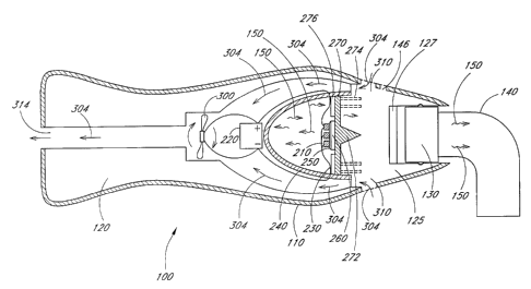
FIGURE 2 shows a cross sectional view of the embodiment shown in FIGURE
1 A.
FIGURE 3 is an exploded view of several optical components and a heat sink
member which form part of the embodiment shown in FIGURES 1A and 2.
FIGURE 4 is a plan view of an LED array resting on the base of the heat sink
member of FIGURES 2 and 3.
FIGURES SA and SB illustrate two preferred configurations of the light source
used in the hand held optical device.
FIGURES 6A, 6B, 6C, and 6D illustrate sequentially how a composite material
within a cavity in a tooth (shown in cross section) is cured so that microgaps
do not
form between the tooth and the cavity.
Detailed Description of the Preferred Embodiment
As shown in FIGURE 1A, the preferred embodiment of the invention
comprises a hand held optical device 100, preferably less than about 20 cm
long
which provides a compact structure that can be used to conveniently deliver
intense
optical radiation, such as laser radiation, to locations which would otherwise
be
difficult to reach. The user grasps the optical device 100 with his or her
hand, and
moves his or her hand to properly orient the light. For example, the optical
device
100 may be used in medical (e.g., surgical) procedures or to cure light
sensitive
material located in tight quarters, such as glue sandwiched between
components.
Also, the device 100 may be used in blood coagulation procedures, in which the
energy density of the optical radiation delivered onto the blood is
advantageously
greater than about 10 J/cm2. The optical device 100 comprises an elongate,
penlight-
shaped housing 110 having a proximal handle portion 120 for aiming the optical
device 100, and a distal receptacle portion. A receptacle 125 in the distal
portion has
an opening which receives and mates with a probe formed by an adaptor 130 and
an
-5-
CA 02370456 2001-10-25
WO 00/67048 PCT/US00/12124
optical element such as an optical lightguide 140, although this optical
element may
also include other optical components such as lenses and filters for changing
the
direction of optical radiation or altering its profile. The bottom of the
receptacle 125
comprises, a protective, optically transparent window 127.. The length of the
adaptor
S 130 is approximately equal to the depth of the receptacle 125 so that the
adaptor is
disposed substantially entirely within the receptacle 125. The optical
lightguide 140,
one end of which is mounted in the adaptor 130, extends from the window 127 to
a
location which is distal of the housing 110. The lightguide 140 is preferably
curved
so as to direct light output from the optical device 100 transversely to the
longitudinal
axis of the handle portion 120. For example, the optical lightguide 140 may be
configured to provide a curved light path suitable for use in an oral cavity,
and may
comprise a few hundred fiber optic strands capable of providing image transfer
quality. The adaptor 130 snaps into and off of the receptacle 125 of the
housing 110.
Thus, the housing 110 can be used with various waveguides or optics of
different
configurations and functionality. The device 100 may optionally include an
optical
mask 142 or 144 for controlling the pattern of optical radiation 150 emitted
by the
device, as discussed in greater detail below.
Referring to FIGURES 2-4, the hand held optical device includes a light source
200. The preferred embodiment 100 comprises an array of diode elements 210
comprised of light emitting diodes (LED) or laser diodes, although the light
source
200 may alternatively comprise a single (non-array) crystal. The diode array
210 is
comprised of a semiconductor material, such as GaN, tailorc9 for a portion of
the
optical spectrum between 300 and 650 nm and collectively may produce from 2 to
1000 mW of output. In one preferred embodiment, the diode elements 210 emit in
the ultraviolet (UV) portion of the spectrum at 365 ~ 30 nm. This wavelength
regime
is suitable for curing glues, such as those used for holding optical
components
together. In another preferred embodiment, the diode elements 210 emit blue
light at
468 ~ 10 nm, which is a spectral regime suitable for chemically activating
camphorquinone, which absorbs at these wavelengths. This compound is a
catalyst
in dental composite materials such as Silux (3M), Bifsil (Bisco), and
Aelitefil (Bisco).
Blue light also overlaps the absorption spectrum of catalysts in dental
resins, and is
-6-
CA 02370456 2001-10-25
WO 00/67048 PCT/US00/12124
useful in various tooth whitening procedures, since blue light is effectively
absorbed
by color centers in teeth. This absorption by color centers leads to localized
heating
within teeth and thus more efficient activation of whitening compounds such as
hydrogen peroxide.
The GaN diode elements 210 may be obtained commercially from Nichia
Chemical Industries (Tokyo, Japan). The individual diode elements 210 are
generally
50 to 500 microns in diameter (or in length, if they are square), and may be
placed
closely together or separated from each other by up to about 150 microns. The
diode
elements 210 are preferably arranged in an array, which may, for example, be a
6 x
6 array of 36 elements, or as few as 9 elements arranged in a 3 x 3 array. The
array
that forms the diode light source 200 is preferably no larger than one square
inch. As
illustrated in FIGURE 2, one or more electrical contact lines 230 for
delivering power
connect the diode elements 210 to a power supply 220, such as a battery (which
may
reside within the housing 110 and is connected to an on/off switch 160) or an
AC
power supply. If a battery is used, it is preferably a rechargeable lithium or
nickel
cadmium battery of about 1-3 amp-hour capacity. A plurality of electrical
contact
lines 230 provide an electrical path from the battery or AC power supply to
the array,
as shown in the 3 x 3 array of FIGURE 4, although just one pair of lines is
shown in
FIGURE 2 for the sake of clarity. The diode elements 210 may have a common
electrical return line (i.e., a single one of the contact lines 230 in FIGURE
4).
Providing the diode elements 210 with several electrical supply lines (rather
than just
one) facilitates stable delivery of current to the diode elements, which is
important
when the output from the diode elements should be in a specific, stable
intensity
pattern. The electrical contact lines 230 pass through a reflector 240 which
receives
the optical radiation 150 emitted by the diode light source 200. In the
embodiment
of FIGURE 4, the array is formed of LEDs and thus, the emission 150 occurs
from
the bottom surfaces as well as the top and side surfaces of the LEDs.
A substrate 250 that is preferably sapphire (semiconductor materials may also
be suitable) underlies the LED array 200. The individual LED elements 210 may
located on a common substrate 240, or each element may have its own substrate.
A
reflecting element 260 in turn underlies the substrate 250 and reflects light
150
CA 02370456 2001-10-25
WO 00/67048 PCT/US00/12124
emitted from the bottom surfaces of the LEDs 210 back towards the reflector
240.
The reflector 240 is contoured to focus light into the optical lightguide 140.
By way
of example, e.g., the reflector may be ellipsoidal in shape. The reflecting
element 260
may be a separate optical component, a coating on the substrate 250, or a
coating on
the base 272.
A heat sink member 270 is positioned at the mouth of the ellipsoidal cavity
formed by the reflecting element 260. The heat sink member 270 is in thermal
contact with the diode light source 200, and conducts heat away from the diode
light
source 200, thereby controlling and stabilizing its temperature and
facilitating stable
power output and better efficiency from the diode light source. The heat sink
member
270 preferably includes a solid tapered base 272 and a plurality of fins 274
which
dissipate heat by conducting it away from the base. As shown in FIGURE 3, the
fins
274 extend radially outward from the base 272 and preferably extend radially
beyond
the reflector 260. Each of the fins 140 lies in a plane substantially parallel
to the
longitudinal axis of the handle so that the fins do not block the reflected
light. The
fins 274 may advantageously be from 0.2-1 mm thick, and from 1 to 50 fins may
be
used. The heat sink member 270 is preferably a high thermal conductivity
material
such as copper, silver, brass, aluminum or stainless steel. The heat sink
member 270
is insulated from the electrical contact lines 230 by a thin layer of
insulating foil 276
such as plastic. The foil 276 may be in the form of thin, long narrow strips
that
separate the fins 274 and the contact lines 230 as shown in FIGURE 3.
Alternatively,
the foil 276 may be a continuous sheet that rests over and extends between the
fins
274 with the contact lines 230 resting on the foil, as in FIGURE 4, in which
case the
foil is transparent to allow passage of the emitted light. Alternatively, the
electrical
contact lines 230 may each have a plastic sheath surrounding them to provide
insulation.
Light 150 emitted from the diode light source 200 is directed by the reflector
240 towards and through the heat sink member 270, and in particular, through
openings between the fins 274 of the heat sink member. The fins 274 are
preferably
reflective at the wavelength of the emitted light 150 so that any light rays
incident
thereon will be efficiently reflected without significant attenuation. The
surfaces of
_g_
CA 02370456 2001-10-25
WO 00/67048 PCT/US00/12124
the fins 274 may be coated, for example, with silver or aluminum to increase
their
reflectivity. The geometrical relationship between the heat sink member 270,
reflecting element 260, the substrate 250, and the diode elements 210 is shown
more
clearly in the exploded view of FIGURE 3.
The various components within the housing 110, including the diode light
source 200, the heat sink member 270, and the reflector 240 may be held in
place
using clamps, fasteners, or other mechanical devices (not shown in the
Figures), as is
known in the art. As shown most clearly in FIGURE 2, the diode light source
200,
the heat sink member 270, and the reflector 240 are mounted in a cavity formed
in the
forward portion of the handle, adjacent the receptacle 125.
To aid in thermal management, a fan 300 may be optionally included in the
housing 110 and may advantageously be powered by the power supply 220. The fan
300 is mounted in a cavity in the handle 120, rearward of the reflector 240.
When
energized, the fan 300 draws in air 304 through one or more air intake ports
310 and
directs the air across the fins 274 of the heat sink member 270 and past the
reflector
240. The air 304 exits the device 100 through an air exhaust port 314.
The optical lightguide 140, such as a fiber optic bundle, receives the emitted
light 150 from the reflector 240 and guides the emitted light to an output end
of the
lightguide 140. The optical lightguide 140 allows the user to direct the
emitted light
into areas that would otherwise be hard to reach. The user grasps the optical
device
100 with his or her hand, and moves his or her hand to properly orient the
light onto
a target area. For example, the optical lightguide 140 may be used to direct
emitted
light 150 onto the tooth of a patient in a tooth whitening procedure.
An alternative embodiment is illustrated in FIGURE 1B, in which the diode
elements 210, the reflector 240, and the heat sink member 270 are all
contained within
a housing 110', which may be positioned on a table, for example. In this case,
the
optical lightguide 140' may be a meter or more in length. The distal end 140a'
of the
optical lightguide 140' may be advantageously curved (like its counterpart
optical
lightguide 140) to permit the user to direct light around corners or into
areas that are
hard to access. In this embodiment, the user manipulates the distal end 140a'
of the
lightguide 140' rather than the entire device.
-9-
CA 02370456 2001-10-25
WO 00/67048 PCT/US00/12124
The optical device 100 may be advantageously used in an office setting having
more than one dental treatment station (not shown), with only one power supply
(not
shown) being used to supply power to one or more of the optical devices. Power
may
be delivered from the power supply through a plurality of power lines (not
shown) to
respective dental stations. One or more of the power lines may be 8 feet long
or
longer. Power from each of the power lines may then be utilized at the
respective
dental stations to energize the diode light source 200 (e.g., the diode array
210) within
the optical device 100 to produce light in the optical range of 400-600 nm,
e.g., blue
light. A light sensitive material (such as a tooth whitening material, a
dental
composite material, or a dental resin) may be applied to a tooth of a patient
at a first
treatment station and then exposed to the light from the diode light source
100. This
procedure may then be repeated on the teeth of other patients at second or
third (or
more) dental stations. This method saves the expense of dedicated power
supplies for
each of the dental stations, and may be used in conjunction with any of the
dental
procedures disclosed herein.
The optical device 100 may be used in other dental procedures as well, such
as the composite curing method described herein, which avoids the formation of
microgaps between a tooth and cured composite material within a cavity in that
tooth.
To this end, the generation of beams of light having circularly and annularly
shaped
cross sections is desirable, as discussed below. More generally, a first beam
has an
intensity distribution that concentrates energy at the periphery of its cross
section,
whereas a second beam does not concentrate energy at thc_ periphery of its
cross
section, for example, the intensity of the second beam is concentrated closer
towards
the center of the cross section, or the intensity of the second beam is evenly
distributed over the cross section.
As shown in FIGURE SA, the diode light source 200' of this embodiment
(which may replace the light source 200 of FIGURES 3 and 4) may advantageously
comprise concentric diode elements 510 and 520, in which either one or both of
the
diode elements 510 and 520 may be turned on at any one time. Thus, if the
diode
element 510 alone is activated, the light source 200' generates an optical
beam that has
a circularly shaped cross section. On the other hand, if the diode element 520
alone
-I 0-
CA 02370456 2001-10-25
WO 00/67048 PCT/US00/12124
is activated, the optical beam generated by the light source 200' has an
annularly
shaped cross section. If both diode elements 510 and 520 are turned on, then
the
optical output has a circularly shaped cross section. Thus, the cross section
of the
light source 200' is variable between first and second patterns.
Alternatively, optical beams with circularly and annularly shaped cross
sections
may be generated with a diode light source 200" like that illustrated in
FIGURE SB,
in which the light source 200" (like its counterpart 200) comprises an array
of diode
elements 210'. For example, by activating diode elements 210' near the center
of the
array (the darkened elements in FIGURE SB), optical output having a cross
section
that approximates a circle can be generated. Likewise, by activating diode
elements
210' closer to the periphery of the array (the undarkened diode elements in
FIGURE
SB), the optical output that is generated has a cross section that
approximates an
annulus. By using a greater number of diode elements 210', a desired intensity
profile
can be approximated more accurately. In each of the embodiments of FIGURES 4,
SA, and SB, the diode elements are located at positions (within the housing
110) that
are fixed with respect to each other, and further, each of the diode elements
is
individually addressable, being connected to a power supply via electrical
contact lines
230 (not shown in FIGURES SA and SB). The output from the light source 200,
200', or 200" can be directed onto tissue (e.g., hard tissue such as a tooth)
by properly
orienting the housing 110 of the optical device 100.
Any of these light sources 200, 200', or 200" can be advantageously used in
the optical device 100 to cure dental composites, as illustrated in FIGURES
6A, B,
C, and D. In FIGURE 6A, an optical beam 605 having a cross section that is
preferably annularly shaped is directed towards a tooth 610. (Both the beam
605 and
the tooth 610 are shown in cross section.) The optical beam 605 preferably
comprises
blue light, as discussed earlier. The tooth 610 has a cavity 620 that is at
least partially
filled with a composite material 630 to be cured. As the annulus-shaped
optical beam
605 strikes the tooth 610, the beam 605 is scattered within the tooth, as
illustrated in
FIGURE 6B. As the scattered optical radiation reaches the portion of the
composite
material 630 that contacts the tooth 610, the composite material 630 begins to
cure.
A layer of cured material 635 forms at the cavity/tooth interface, whereas the
CA 02370456 2001-10-25
WO 00/67048 PCT/US00/12124
composite material that is situated within the cavity 620 and away from the
tooth 610
(e.g., at the center of the cavity) remains uncured.
After the layer of cured material 635 has been formed, the composite material
630 that remains uncured (i.e., the composite material in the interior portion
of the
cavity 620) may be cured by directing a second optical beam 640 (with a cross
section
that is preferably circular in shape) towards the composite material within
the cavity
620, as illustrated in FIGURE 6C. The second optical beam 640 has a cross
section
that illuminates the composite material 630 more uniformly than does the first
optical
beam 640. For example, the second optical beam may advantageously cover the
entire
tooth 610, or only the cavity 620 as indicated in FIGURE 6C. The remaining
uncured
composite material 630 (i.e., within the interior of the cavity 620) is thus
cured,
resulting in a cavity filled with cured composite material 635, as illustrated
in
FIGURE 6D. The first and second optical beam patterns used in the disclosed
curing
method are generated upstream of the lightguide 140. It is preferable to
utilize a
bundle of fiber optic lightguides that have constant relative orientation
throughout the
length of the lightguide, so that the pattern of the beams' respective cross
sections
does not vary as the beams propagate through the lightguide, and so that the
beams
propagate along a common optical path towards the target area.
One advantage of the method discussed in connection with FIGURES 6A-D
is that the formation of microgaps between the tooth 610 and the cured
composite
material 635 is inhibited, thereby reducing the chance that secondary caries
are
formed. The technique disclosed herein is a general one that can be employed
to
control the direction of shrinkage of light cured composite materials by
suitably
tailoring the pattern of the cross section of an optical beam.
As an alternative to the light source 200 directly producing optical beams
with
a particular shape, a wide area circular beam may be used. For example, all of
the
diode elements 210 or 210' may be turned on, and the optical masks 142 and 144
of
FIGURE 1A may be used to generate optical beams having circularly and
annularly
shaped cross sections, respectively. The mask 142 (or 144) may be inserted
through
a groove 146 in the housing 110, slipped into another groove (not shown)
within the
housing, and then held in place with a clip (not show) advantageously located
on the
-12-
CA 02370456 2001-10-25
WO 00/67048 PCT/US00/12124
outside of the housing. In yet another embodiment, an optical beam with an
annularly
shaped cross section may be generated from a beam with a circularly shaped
cross
section (or vice versa) by using an appropriate set of optical components
(such as
lenses, not shown) between the diode light source 200 and the lightguide 140,
in
which at least one or more optical components is movable to permit the user to
choose
a particular pattern. Such an embodiment is necessarily longer than the one
illustrated
in FIGURE 1 A.
The optical source disclosed herein can be used in a variety of other methods,
including, for example, whitening a darkened tooth or teeth. Such a method
preferably comprises: preparing the teeth and gums, applying a whitening
solution to
the teeth, exposing the teeth to light, cleaning the exposed teeth, and
exposing the
cleaned teeth to one or more sodium fluoride treatments to help the teeth
retain their
whitened color.
First, the teeth and gums are prepared. The teeth to be whitened should be
isolated from the gums and the rest of the mouth with a rubber dam which can
be
painted on the areas to be protected. Ligature floss or a specialty product
(block out
compound) can be used to form a tight cuff that will protect the gums. Each
tooth
should then be rubbed for about 5-10 seconds with a mixture of 35% hydrogen
peroxide (or carbamide peroxide)/balance pumice, although care must be taken
to
avoid splattering any of this mixture into the patient's face or eyes. The
teeth should
not be rinsed with water after pumicing but rather wiped off with a gauze
sponge.
After the teeth have been prepared, a whitening material in the form of a
solution or paste should be applied to each tooth to be whitened. A variety of
compounds may be used for this purpose, many of which are commercially
available
from firms such as Interdent (which manufactures QuaserBrite whitening
substance),
Shofu (Hi-Lite and Blulite whitening substance), DenMat (QuickStart whitening
substance), and LoChemCo (Varishade). Whitening materials can also be made
from
batch starting materials, such as hydrogen peroxide, carbamide peroxide, and
silicon
dioxide. The whitening material is preferably 35-50% hydrogen or carbamide
peroxide. Other compounds such as silicon dioxide can be added to the peroxide
to
-13-
CA 02370456 2001-10-25
WO 00/67048 PCT/US00/12124
form a suspended mix or paste-like substance which has the advantage of being
easy
to apply.
Next, the teeth are exposed to optical radiation ("activating light"), which
has
the effect of accelerating the chemical reactivity of the peroxide solution.
The best
results are obtained if the whitening material is first allowed to seep into
each tooth
for a substantial period of time, e.g., at least 20-60 seconds. The source of
this optical
radiation is preferably a CW (continuous wave) or nearly CW laser in the
optical
range 400-600 nm, or more preferably 450-510 nm, i.e., optical radiation in
the blue
portion of the electromagnetic spectrum, such as the argon ion laser line near
488 nm,
frequency doubled output from near-infrared emitting diode lasers, or the blue
optical
source disclosed herein. Continuous wave laser output having an average power
of
300-350 mW (although satisfactory results may also be obtained over the range
100-
600 mW) is preferably directed continuously for 20-40 seconds on each tooth.
Laser
light should not be directed to any one tooth for an arbitrary length of time,
since
extended exposure to laser energy heats the tooth, and vitality of the pulp is
reduced
if the tooth is heated too much. Preferably, the total laser energy directed
to each
tooth is no greater than 14 joules per application of laser energy.
After the laser treatment, the irradiated teeth should be cleaned, preferably
using a water syringe. If insufficient whitening is observed, it may be
desirable to
repeat the whitening process by again applying whitening material to the teeth
and
again exposing this material to laser light. A maximum of three
application/exposure
cycles is preferred.
At this point, a neutral sodium fluoride gel should be applied to the teeth,
with
each tooth being polished with a burnishing burr, polishing cups, or discs for
about
15 seconds. In addition, it is recomrr~ended that, following the treatment,
the patient
wear a tray with sodium fluoride suspension for about four hours on the day of
the
whitening procedure.
Most patients will experience a two to three shade improvement in tooth color
for a single application/exposure cycle, although some patients may need to
undergo
the procedure two times. Regular use of a whitening tooth paste such as
Colgate
-14-
CA 02370456 2001-10-25
WO 00/67048 PCT/US00/12124
Platinum or Den-Mat's Rembrandt will reduce re-darkening of the teeth
following the
whitening procedure disclosed herein.
The optical source disclosed herein may also be used in connection with a
method in which a dental composite material or a dental resin material is
applied to
a tooth. The array of diodes 210 may be utilized to produce activating light
having
a wavelength in the range 400-600 nm, and the activating light is applied to
the dental
composite or resin material at a power level of 100-200 mW for a period of 2-S
seconds. The activating light may be advantageously applied to the material
for about
3 seconds, and the activating light is preferably applied continuously to the
tooth or
teeth to be treated. A power level of about 150 mW may advantageously be used.
The invention may be embodied in other specific forms without departing from
its spirit or essential characteristics. The described embodiments are to be
considered
in all respects only as illustrative and not restrictive. The scope of the
invention is
therefore indicated by the appended claims rather than by the foregoing
description.
All changes which come within the meaning and range of equivalency of the
claims
are to be embraced within that scope.
-IS-