Note: Descriptions are shown in the official language in which they were submitted.
CA 02370546 2001-11-26
WO 01/80511 PCT/USO1/05134
-1-
Description
PHASE NOISE AND ADDITIVE NOISE ESTIMATION IN A QAM CARRIER RECOVERY CIRCUIT
TECHNICAL FIELD
The present invention relates to a quadrature
amplitude modulation (QAM) type demodulator for demodu-
lating signals modulated in accordance with the QAM
scheme.
BACKGROUND ART
Quadrature amplitude modulation (QAM) is an
intermediate frequency (IF) modulation scheme in which a
QAM signal is produced by amplitude modulating two base-
band signals, generated independently of each other, with
two quadrature carriers, respectively, and adding the
resulting signals. The QAM modulation is used to modu-
late a digital information into a convenient frequency
band. This may be to match the spectral band occupied by
a signal to the passband of a transmission line, to allow
frequency division multiplexing of signals, or to enable
signals to be radiated by smaller antennas. QAM has been
adopted by the Digital Video Broadcasting (DVB) and Digi-
tal Audio Visual Council (DAVIC) and the Multimedia Cable
Network System (MCNS) standardization bodies for the
transmission of digital TV signals over Coaxial, Hybrid
Fiber Coaxial (HFC), and Microwave Multi-port Distribu-
tion Wireless Systems (MMDS) TV networks.
The QAM modulation scheme exists with a vari-
able number of levels (4, 16, 32, 64, 128, 256, 512,
1024) which provide 2, 4, 5, 6, 7, 8, 9, and 10
Mbit/s/MHz. This offers up to about 42 Mbit/s (QAM-256)
over an American 6 MHz CATV channel, and 56 Mbit/s over
an 8 MHz European CATV channel. This represents the
CA 02370546 2001-11-26
WO 01/80511 PCT/USO1/05134
-2-
equivalent of 10 PAL or SECAM TV channels transmitted
over the equivalent bandwidth of a single analog TV pro-
gram, and approximately 2 to 3 High Definition Television
(HDTV) programs. Audio and video streams are digitally
encoded and mapped into MPEG2 transport stream packets,
consisting of 188 bytes.
The bit stream is decomposed into n bits pack-
ets. Each packet is mapped into a QAM symbol represented
by two components I and Q, (e. g., n=4 bits are mapped
into one 16-QAM symbol, n=8 bits are mapped into one 256-
QAM symbol). The I and Q components are filtered and
modulated using a sine and a cosine wave (carrier) lead-
ing to a unique Radio Frequency {RF) spectrum. The I and
Q components are usually represented as a constellation
which represents the possible discrete values taken over
in-phase and quadrature coordinates. The transmitted
signal s{t) is given by:
s { t) =Icos (2nfot) -Qsin (2rtfot) ,
where fo is the center frequency of the RF signal. I and
Q components are usually filtered waveforms using raised
cosine filtering at the transmitter and the receiver.
Thus, the resulting RF spectrum is centered around fo and
has a bandwidth of R(1+ot), where R is the symbol trans-
mission rate and cx is the roll-off factor of the raised
cosine filter. The symbol transmission rate is 1/nt'' of
the transmission bit rate, since n bits are mapped to one
QAM symbol per time unit 1/R.
In order to recover the baseband signals from
the modulated carrier, a demodulator is used at the re-
ceiving end of the transmission line. The receiver must
control the gain of the input amplifier that receives the
signal, recover the symbol frequency of the signal, and
recover the carrier frequency of the RF signal. After
CA 02370546 2001-11-26
WO 01/80511 PCT/USO1/05134
-3-
these main functions, a point is received in the I/Q
constellation which is the sum of the transmitted QAM
symbol and noise that was added over the transmission.
The receiver then carries out a threshold decision based
on lines situated at half the distance between QAM sym-
bols in order to decide on the most probable sent QAM
symbol. From this symbol, the bits are unmapped using
the same mapping as in the modulator. Usually, the bits
then go through a forward error decoder which corrects
possible erroneous decisions on the actual transmitted
QAM symbol. The forward error decoder usually contains a
de-interleaver whose role is to spread out errors that
could have happened in bursts and would have otherwise
have been more difficult to correct.
Generally, in transmitting a modulated signal,
two impairments are encountered, phase noise and additive
noise. Phase noise is generated by the various mixers
and local oscillators in the modulator and the demodu-
lator. The sidebands of the phase noise signal are co-
herent, which means that the upper frequency sidebands
have a definite phase relationship to the lower frequency
sidebands. Additive noise, also referred to as additive
gaussian white noise, is random noise that has a fre-
quency spectrum that is continuous and uniform over a
specified frequency band. It is often very difficult to
evaluate the amount of phase noise or additive noise for
which the demodulator should compensate. In order to
compensate for phase noise, the carrier loop bandwidth
has to be increased. However, this causes the signal
degradation caused by the additive noise to increase. In
order to compensate for the additive noise, the carrier
loop bandwidth should be decreased, but this causes the
effect of increasing the phase noise degradation of the
signal.
CA 02370546 2001-11-26
WO 01/80511 PCT/USO1/05134
-4-
In the prior art, several attempts have been
made to compensate for or to eliminate phase noise and/or
additive noise. U.S. Patent No. 5,315,618 to Yoshida
discloses a method and apparatus for cancelling periodic
carrier phase fitter. In the Yoshida invention, if a
demodulated complex baseband signal is deviated in phase
from a QAM signal point due to phase fitter, the phase
error is detected, and a replica of the phase fitter is
calculated and applied to impart phase rotation for
cancelling out the phase fitter that is contained in the
complex baseband signal. U.S. Patent No. 4,675,613 to
Naegeli et al. discloses a circuit in a synchronous de-
tector system that is provided to minimize and compensate
for the errors induced by phase modulation and additive
noise in the system. In one embodiment, a first-order
correction of such errors is achieved by equipping the
synchronous detector system with a phase lock loop having
a constant loop filter noise bandwidth to reduce the
phase noise and an RMS detector for first order correc-
tion of the additive noise. The resolution filter pass-
ing the signal to the RMS detector is made to have a
noise bandwidth identical to the loop noise bandwidth.
U.S. Patent Nos. RE 31,351 and 4,213,095 to Falconer
discloses, respectively, a feedback nonlinear equaliza-
tion of modulated data signals and a feedforward nonlin-
ear equalization of modulated data signals. In the '351
patent, a receiver for a QAM signal impaired by linear
and non-linear distortion, phase fitter and additive
noise includes circuitry which compensates for these
impairments. In particular, the receiver includes a
processor which subtracts a feedback nonlinear signal
from each sample of the received signal, either prior to
or subsequent to demodulation, providing compensation for
non-linear intersymbol interference. In the '095 patent,
a feedforward non-linear signal is added to each sample
CA 02370546 2001-11-26
WO 01/80511 PCT/USO1/05134
-5-
of a linearly equalized received signal to provide com-
pensation for nonlinear intersymbol interference. In
each of the patents, the feedback/feedforward nonlinear
signal is comprises of a weighted sum of products of
individual ones of the samples and their complex conju-
gates.
It is an object of the present invention to
provide a QAM type demodulator that provides a joint
estimation of the phase noise and the additive noise,
while limiting the mutual effect induced by one of the
estimations on the other of the estimations. '
SUMMARY OF THE TNVENTION
The above object has been achieved by a QAM
demodulator having a carrier recovery circuit that in-
cludes a phase estimation circuit and an additive noise
estimation circuit which produces an estimation of the
residual phase noise and additive noise viewed by the QAM
demodulator. The invention makes it possible to estimate
the required information in the field in order to opti-
mize the carrier loop bandwidth and to reach the best bit
error rate possible. This information can be used to
select the carrier loop bandwidth that provides the best
trade off between phase noise and additive noise. The
phase noise estimation is based on the least mean square
error between the QAM symbol decided by a symbol decision
circuit and the received QAM symbol. The error is based
only on QAM symbols having the maximum amplitude on I and
Q coordinates. The additive noise estimation is based on
the same error as in the phase noise estimation, except
that it is based only on QAM symbols having the minimum
amplitude on the I and Q coordinates. The additive noise
estimator is not dependent on the phase of the signal.
CA 02370546 2001-11-26
WO 01/80511 PCT/USO1/05134
-6-
BRIEF DESCRIPTION OF THE DRAWTNGS
Fig. 1 is a block diagram of a Network Inter-
face Unit in which the demodulator of the present inven-
tion may be used.
Fig. 2 is a block diagram of the demodulator of
the present invention.
Fig. 3 is a block diagram of the first AGC unit
of the demodulator shown in Fig. 2.
Fig. 4 is a block diagram of the second AGC
unit of the demodulator shown in Fig. 2.
Fig. 5 is a block diagram of a section of the
demodulator shown in Fig. 2.
Fig. 6 is a block diagram of the Direct Digital
Synthesizer of the demodulator shown in Fig. 2.
Fig. 7 is a block diagram of the digital timing
recovery circuit of the demodulator shown in Fig. 2.
Fig. 8 is a block diagram of a generally known
interpolation model.
Fig. 9 is a block diagram of an interpolation
model used in the digital timing recovery circuit of Fig.
7.
Fig. 10 is a block diagram of a phase noise and
additive noise estimator used in the symbol detection
circuit of the demodulator of Fig. 2.
Fig. 11 is a block diagram of the Dual Bit
Error Rate estimator used in the demodulator of Fig. 2.
BEST MODE FOR CARRYING OUT THE INVENTION
With reference to Fig. 1, the QAM demodulator
99 of the present invention would typically be used as
part of a Network Interface Unit 92. The Network Inter-
face Unit 92 is defined as the interface block between a
signal 95 received from a Cable Network and the input
signal 93 of a demultiplexer. The signal 95 from the
cable network is input into a tuner 96. The tuner ac-
CA 02370546 2001-11-26
WO 01/80511 PCT/USO1/05134
Cepts frequencies in the range of 47 MHz to 862 MHz at
its input and down converts the selected frequency to an
intermediate frequency (IF). This IF frequency depends
on the channel bandwidth as related to the geographic
location. For example, NTSC, USA and JAPAN have a 6 MHz
channel with IF around 44 MHz, while PAL/SECAM and EUROPE
have an 8 MHz channel with IF around 36 MHz. The output
of the tuner is input to a surface acoustic wave (SAW)
filter 97, the IF frequency being equal to the SAW filter
l0 center frequency. The output of the SAW filter 97 is
supplied to an amplifier 98, which is used to compensate
for the SAW filter attenuation, and then the output of
the amplifier 98 is supplied to the QAM demodulator 99.
The amplifier 98 can also have a variable gain controlled
by an Automatic Gain Control signal 94 of the QAM demodu-
lator 99. It is also possible for the QAM demodulator 99
to be used in various other digital transmission systems
using QAM or QPSK demodulation, such as radio links,
wireless local loops, or in-home networks.
Referring to Fig. 2, the QAM demodulator 99 of
the present invention includes an analog-to-digital (A/D)
converter 25 which receives the IF input signal 12. The
A/D converter 25 samples the IF signal 12 and produces a
digital spectrum around the center frequency Fo of the IF
signal 12. The output signal 14 of the A/D converter 25
is supplied to a baseband conversion circuit that in-
cludes a Direct Digital Synthesizer 30 in order to Con-
vert the IF signal to a baseband signal. The output
signal 14 of the A/D converter 25 is also supplied to the
first Automatic Gain Control circuit (AGC1) 10 for Con-
trolling the analog gain of the input signal 12 of the
A/D converter 25.
After the signal has been converted to a base-
band signal having signal components I (inphase) and Q
(quadrature), the baseband signal is supplied to a timing
CA 02370546 2001-11-26
WO 01/80511 PCT/USO1/05134
-g_
recovery circuit 35 which is used to synchronize the
timing of the demodulator circuit to the symbols of the
incoming signals. The timing recovery circuit 35 uses a
continuously variable interpolation filter for sampling
the input signal which allows the circuit to recover a
very large range of symbol rates, as will be further
explained below. The signal is then supplied to a digi-
tal multiplier 210 which is part of a second Automatic
Gain Control (AGC2) circuit 20. Then, the signal goes
20 through a Receive Filter 40 and then to an Equalizer 45.
The AGC2 circuit 20 is a digital AGC circuit and performs
a fine adjustment of the signal level at the equalizer 45
input. The digital AGC circuit 20 only takes into ac-
count the signal itself, since adjacent channels have
been filtered out by the receive filter 40, and thus
compensates digitally for the analog AGC1 circuit 10
which may have reduced the input power due to adjacent
channels. The receive filter 40 is a squared root raised
cosine type which supports roll-off factors from 0.11 to
0.30, which accepts the timing recovery circuit output
signal and ensures an out-of-band rejection higher than
43dB. This significant rejection increases the back off
margin of the Network Interface Unit against adjacent
channels. The equalizer 45 compensates for different
impairments encountered on the network, such as undesired
amplitude-frequency or phase-frequency response. Two
equalizer structures can be selected, Transversal or
Decision feedback with selectable central tap position.
The output signals of the equalizer 45 are
supplied to the carrier recovery circuit 50 to recover
the carrier signal. The carrier recovery circuit 50
allows the acquisition and tracking of a frequency offset
as high as 12 percent of the symbol rate. The frequency
offset recovered can be monitored through a I2C inter-
face. This information can be used to readjust the tuner
CA 02370546 2001-11-26
WO 01/80511 PCT/USO1/05134
-9-
or the demodulator frequency in order to reduce the fil-
tering degradation of the signal, which helps to improve
the bit error rate. The output signal 52 of the~carrier
recovery circuit 50 is supplied to a symbol decision
circuit 55 and is also supplied to a Power Comparator
Circuit 230 and Digital Loop Filter 220 within the digi-
tal AGC2 circuit 20 to provide a gain control signal 225
to the multiplier 210. Within the symbol decision. cir-
cuit 55, the signal is supplied to a symbol threshold
detector, then to a differential decoder, and finally to
a DVB or DAVIC de-mapper which produces the recovered bit
stream 57 sent to the Forward Error Correction Circuit
60. The output 57 of the symbol decision circuit is also
supplied to the Power Comparator Circuit 230.
The Forward Error Correction (FEC) circuit 60
first performs a frame synchronization 61 in which the
bit stream is decomposed into packets of 204 bytes at the
output. The packets are then supplied to a de-
interleaver and Reed-Solomon (RS) decoder 65, where the
packets are de-interleaved and then a correction is per-
formed by the RS decoder of a maximum of 8 errors (bytes)
per packet. The RS decoder also provides other informa-
tion regarding the uncorrected packets and the position
of the corrected bytes in the packet, if there are any.
Two depths can be selected for the interleaver: 12
(DVB/DAVIC) and 17. The depth 17 increases the strength
of the system against impulse noise, but assumes that the
signal has been interleaved with the same value at the
monitor. After RS decoding, the packets are de-scrambled
for energy dispersal removal. The data output 93 of the
FEC circuit 60 is constituted of the MPEG2 Transport
System (TS) packets and is the output of the demodulator
99. Additionally, bit error rate signals 68, 69 are
transmitted to a Dual Bit Error Rate Estimator circuit 70
which estimate Low and High Bit Error Rates based on
CA 02370546 2001-11-26
WO 01/80511 PCT/USO1/05134
-10-
error correction and frame pattern recognition and pro-
duces a Bit Error Rate Signal 72.
As explained above, the dual automatic gain
control (AGC) circuits are situated before and after the
receive filters to control the received level of the
signal. The first AGC circuit 10 controls the analog
gain of the input signal of the A/D converter. With
reference to Fig. 3, the output signal 14 of the A/D
converter 25 is supplied to a power estimation circuit
110 of the AGC1 10 in order to estimate the signal level
of the received signal 14 and compare it to a predeter-
mined signal level. The power estimation circuit 110
includes a square module 130 for converting the signal 14
into a square wave to be input into a comparator 140.
The comparator 140 compares the input signal with a pre-
determined reference voltage, or comparator threshold
voltage, and produces an output signal when the level of
the input signal matches the level of the comparator
threshold voltage. The comparator threshold voltage, or
reference voltage, can be adapted by a modification cir-
cuit 120. The modification circuit 120 monitors the
presence of signals from adjacent channels 125 and adapts
the reference voltage accordingly. Additionally, a de-
tection of saturation counter 115 detects whether there
is any saturation in the A/D converter and, if so, sends
a signal to the modification circuit 120 in order to
adjust the reference voltage in order to eliminate the
saturation. After the signal goes through the comparator
140, the output signal of the power estimator circuit 110
is supplied to a digital loop filter 150 which removes
the carrier-frequency components and harmonics from the
signal, but passes the original modulating frequencies of
the signal. The digital loop filter 150 receives a con-
figuration signal 152 which sets the amplifier maximum
gain configuration for limiting non-linearities. The
CA 02370546 2001-11-26
WO 01/80511 PCT/USO1/05134
-11-
output signal 162 of the digital loop filter 150 is con-
verted to a Pulse Width Modulated (PWM) signal 160 which
is supplied to an RC filter 170 which produces a signal
167 that controls the analog gain of the amplifier of the
A/D converter. Another output of the digital loop filter
provides a signal 155 for monitoring the gain value of
the digital loop filter. Since the power estimation is
estimated by the digital loop control, the PWM signal
that controls the analog gain generates very stable con-
trol.
The second AGC circuit 20 is situated after the
receive filter 40, therefore only having to take into
account the received power of the QAM signal itself, and
adapts the internal amplification level to the correct
level before threshold decision. The second AGC circuit
compensates for the attenuation of the first AGC cir-
cuit 10, which is caused by the presence of adjacent
channels, and also adapts the signal level exactly to the
decision threshold levels of the QAM signal. With refer-
20 ence to Fig. 4, the output signal 42 of the timing recov-
ery circuit is supplied to the digital multiplier 210 of
the second AGC circuit 20. The digital multiplier 210
multiplies the signal, which is then supplied to the
receive filter 40, equalizer 45 and carrier recovery 50
circuits as explained above. The output of the carrier
recovery circuit 50 is fed back into a power comparator
circuit 230 of the second AGC circuit 20 which compares
the output signal 52 from the carrier recovery circuit
with a set of QAM values. A digital loop filter 220
filters out any error signals and provides a gain control
signal 225 to the digital multiplier 210. Additionally,
a signal 227 can be provided from the digital loop filter
in order to monitor the amount of gain.
With reference to Figs. 5 and 6, the aforemen-
tinned Direct Digital Synthesizer (DDS) 30 digitally
CA 02370546 2001-11-26
WO 01/80511 PCT/USO1/05134
-12-
tunes the signal 14 from the A/D converter 25 to be
within the bandwidth of the receive filter 40 even in the
case of a large frequency offset of the receiver and
provides more flexibility in the frequency values used by
the input signal. The Intermediate Frequency (IF) to
baseband signal conversion is accomplished by using a
combination of a first DDS 30 before the receive filter
40 in order to digitally tune the signal within the re-
ceive filter bandwidth, and a second DDS 545 within the
carrier recovery circuit 50 to fine tune the signal phase
after the timing recovery 35 and equalizer 45 circuits.
Referring to Fig. 6, after the IF signal 12
passes through the A/D converter 25, the output digital
signal 14 of the A/D converter is supplied to a multi-
plier 304 that is part of DDS1 30. The multiplier 304
converts the digital signal 14 into two parallel compo-
nents, I (inphase) and Q (quadrature) which form a QAM
symbol. These signal components proceed through the
receive filter 40, equalizer 45 and carrier recovery 50
circuits, as explained above. Referring to Fig. 5, the
carrier recovery circuit 50 includes a frequency offset
detect 525 circuit and a phase offset detect 535 circuit
for recovering the carrier signals to be sent to the
digital AGC2 circuit 20 and the symbol detection circuit
55. The frequency offset recovered can be monitored
through an I2C interface and the information can be used
to readjust the tuner frequency in order to reduce the
filtering degradation on the signal and thus improve the
bit error rate. This information can also be sent as a
signal 527 to the DDS1 circuit 30 in order to recover the
frequency with complete accuracy before the receive fil-
ter 40. The phase detect circuit 535 sends a signal 537
to the DDS2 circuit 545. Employing a dual DDS structure
to control the down conversion of the IF signal to a
baseband signal is advantageous in that the long loop
CA 02370546 2001-11-26
WO 01/80511 PCT/USO1/05134
-13-
frequency down-conversion is optimal for frequency recov-
ery since it is done before the receive filter 40 in
order to maintain the maximum signal energy before equal-
ization and carrier frequency estimation, while the short
loop carrier phase recovery is optimal for phase track-
ing, especially in case of phase noise on the signal.
Referring to Fig. 6, the carrier recovery fre-
quency feedback signal 527 is supplied to an adder cir
cuit 306 within the DDS1 circuit 30. The adder circuit
306 adds the frequency feedback signal 527 to the config
ured IF frequency 27 and the resulting signal is supplied
to a phase accumulation circuit 305 which accumulates
frequency elements determined by the frequency feedback
signal 527. The signal is supplied to a constant table
303 containing sinusoidal values which synthesizes the
signal. The synthesized signal 316 is supplied back into
the multiplier 304. Referring back to Fig. 5, the second
DDS2 circuit 545 operates in the same manner except that
it synthesizes the output signal 537 of the phase detect
circuit 535. The purely digital carrier recovery elimi-
nates the need for a voltage controlled oscillator (VCO)
to be used and provides a better carrier recovery in
terms of accuracy and the residual phase noise of the
signal.
With reference to Fig. 7, the timing recovery
circuit 35 uses a symbol rate continuously adaptive in-
terpolation filter 352 for resampling the input signal.
As opposed to prior art methods of interpolation which
use interpolation functions which are defined as function
of t/TS (time/sampling Interval), the method of interpola-
tion used in the timing recovery circuit 35 is defined as
a function of t/Ti (time/Interpolation Interval). This
allows the interpolation filtering to be totally inde-
pendent of the symbol rate in terms of performance and
complexity and provides a better rejection of adjacent
CA 02370546 2001-11-26
WO 01/80511 PCT/USO1/05134
-14-
channels since the interpolator rejects most of the sig-
nal outside the bandwidth of the received channel.
The objective of interpolation in modem appli-
cations is to process. digital samples x(kTs) 325 produced
by an analog to digital converter at rate 1/TS, in order
to generate "interpolants" y(kTi) 365 at rate 1/Ti, with
1/Ti multiple of the transmission baud rate 1/T.
The following will describe interpolation with
a time-continuous filter. The mathematical model is
.10 described with reference to Fig. 8. It includes a ficti-
tious digital to analog converter 802 which produces
analog impulses 814, followed by a time-continuous filter
h(t) 804, and a resampler 806 at time t = kTi. The output
interpolants 820~are represented by
y(kTi) _~ x (mTs) h (kTi-mT$) (1)
m
Referring back to Fig. 7, the resample - in-
stants t = kTi are delivered by a numerically controlled
oscillator 358. The numerically controlled oscillator
358 produces two signals at each time mTs. The first
signal 361 is an overflow signal ~, which indicates that
a resample instant (t = kTi) has occurred during the last
TS period. The second signal 362 is a Ti-fractional
signal r~, such that x~Ti represents the time since the
last resample instant.
The numerically controlled oscillator 358 is
controlled by a signal W(m) which estimates the ratio
TS/Ti. In practical modem applications, W(m) is delivered
by a loop filter 356 driven by a phase error estimator or
timing error detector 354.
The mathematical description of this can be
written with formula:
CA 02370546 2001-11-26
WO 01/80511 PCT/USO1/05134
-15-
x~ (m) _ [~ (m-1) -W(m) ] mod -1
~ (m) = 1 if ~ (m-1 ) -W (m) <0 ( 2 )
~ (m) = 0 if r~ (m-1) -W(m) z0
Prior interpolation methods, which use a filter
h(t) normalized by the sampling period TS, introduce a TS
basepoint index and a TS fractional interval. In the
interpolation method used by the present invention, for
mula (1) above is rewritten with h being a function of a
variable r~~Ti. This property of the function h allows
the timing and frequency response of the interpolation to
be invariant with respect to the interpolants rate, and
thus with respect to the baud rate. To achieve this,
first note that the sampling instants mTs can be written
as follows:
mTs = lm Ti -T~ (m) Ti
where r~(m) is the direct output of the nco and (lm-1) is
the number of overflows (~ = 1) since t=0 up to time
t=mTs. Introducing the integer interval I1 that contains
all m such that lm l, formula (1) can now be written as
follows:
y(kTi) _ ~ ( ~ X(mTs) ~ h[ (k-1+r~ (m) ) Ti] ) (3)
1 mEh
Assuming that h(t) is a finite length impulse response
over the interval [IlTz, IZTi] , formula (3) is rearranged
with index j - k-l:
I
Y(kTi) - ~ a~ L (k-j) Ti]
I1
with:
a~ (1Ti) - ~ x (mTs) ~h [ (j+~l (m) ) Ti]
mEh
CA 02370546 2001-11-26
WO 01/80511 PCT/USO1/05134
-16-
The latest formula shows that the interpolants are com-
puted by summing and delaying ( I1+Iz+~. ) terms a~ ( 1Ti ) ,
where a~(lti) is the accumulation over the time interval
[1-1)Ti, 1Ti] of the multiplication of input samples
x(mTs) by coefficients h[ (j+r~ (m) )Ti] .
With reference to Fig, 9, aj is practically
implemented with a multiplicator-accumulator operator 908
which is reset when the overflow signal Vi(m)=1. A coef-
ficient h[ (j+r~ (m) )Ti] is delivered by a coefficient-
computation block 909 with an input 1~(m) being output by
the numerically controlled oscillator (NCO) 910.
It is noted that the multiplier-accumulators
operate at frequency 1/T5 and that the sum of aj is com-
puted at frequency 1/Ti. For a low ratio TS/Ti, a high
number of multiplication-accumulations are processed
during a long Ti period. This allows the Ti -
interpolator to have a longer time impulse response in
regards to TS, and a narrower frequency bandwidth in
regards to sampling frequency.
2 0 For practical reasons, h [ ( j +r~ ) Ti] may be poly
nomial function of r~ over the interval [0,1], and
h [ ( j +r~ ) Ti] =p~ (r~ ) . Polynomials of degree 3 have been
chosen for a practical implementation because this is of
reduced computation complexity and allows very good per-
formances for the impulse response h(t), with only a few
intervals Ti (typically 4 to 8). A particular form of the
polynomials can also be used to further reduce the compu-
tational complexity. Once the degree, form and number
(I1+IZ+1) of polynomials is chosen, the parameters of the
polynomials are computed by minimizing a cost function
that represents the spectral constraints on the impulse
response h(t).
It is also noted that the variable x~, used for
computing the coefficient h[ (j+r~ (m) )Ti] , does not need
CA 02370546 2001-11-26
WO 01/80511 PCT/USO1/05134
-17-
any additional computation and approximation, as is the
case for prior art TS - interpolation methods.
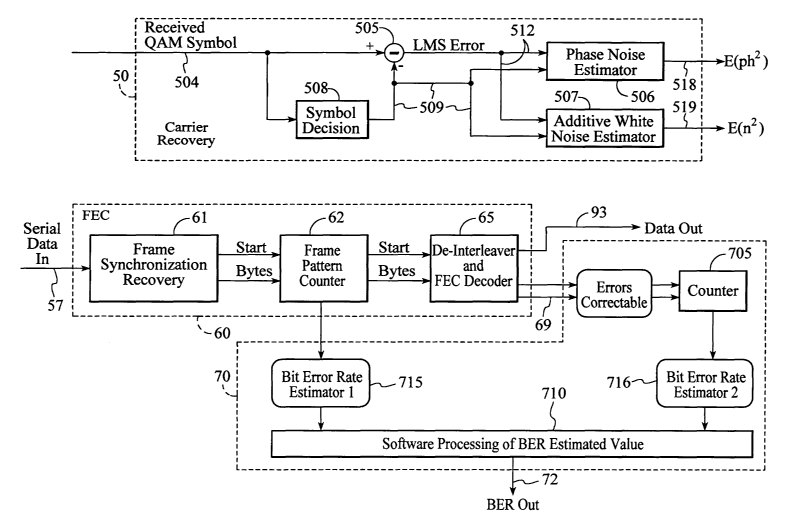
With reference to Fig. 10, the previously de-
scribed carrier recovery circuit 50 includes a phase
noise estimation circuit 506 and an additive noise esti-
mation circuit 507 which produces an estimation of the
residual phase noise and additive noise viewed by the Q.AM
demodulator. This estimation allows the user to optimize
the carrier loop bandwidth in order to reach the best
trade off between the phase noise and the additive noise.
The received QAM symbol 504 is supplied to a symbol de-
tection or decision block 508. The received QAM symbol
504 is a point in I/Q coordinates which is close in terms
of distance to a possible transmitted QAM symbol, but is
different because of noise. The symbol detection block
508 decides on the most probable transmitted QAM symbol,
by searching for the minimum distance between the re-
ceived QAM symbol and possible transmitted QAM symbols
(threshold symbols). In this way, the symbol detection
block 508 determines which QAM symbol was transmitted.
The Least Mean Square (LMS) error between the decided QAM
symbol 509 and the received QAM symbol 504 is determined
by the LMS error method 505 as known in the art and the
LMS error signal 512 is supplied with the decided QAM
symbol 509 to each of the phase noise 506 and additive
noise 507 estimators.
The phase noise estimation is based on the
least mean square error (dx+jdy), where dx+jdy = (re-
ceived point - decided QAM symbol). This~error is con-
sidered only for QAM symbols having the maximum and same
amplitude on I and Q (~a~ + j~a~). The mean phase noise is
then given by E[dx*dy]=-~a~2 E(ph2), where E represents the
mean and ph is the residual phase noise. The phase noise
estimator result 518 does not depend on the additive
noise.
CA 02370546 2001-11-26
WO 01/80511 PCT/USO1/05134
-18-
The additive noise estimation is based on the
same error signal 512 as in the phase noise estimation,
but the error in the case of noise estimation is based
only on QAM symbols having the minimum amplitude (~a~=1)
on I and Q. The mean additive noise is given by
E[dx*sgn(I)*I+dy*sgn(Q)*Q)2] - E[n~], where n denotes the
complex additive noise. The additive noise estimator
result does not depend on the phase of the signal.
With reference to Fig. 11, the recovered bit
stream 57 from the aforementioned symbol detection cir-
suit is supplied to a Frame Synchronization Recovery
(FSR) circuit 61 within the Forward Error Correction
(FEC) decoder 60. The FSR circuit 61 decomposes the bit
stream into packets of 204 bytes at the output. Then,
the packets are supplied to a Frame Pattern. Counter 62
which maintains a count of recognizable patterns of the
frame over a sufficiently large number of frames in order
to obtain additional information, such as synchronization
patterns, that is not encoded by the FEC encoder. This
information is input into a first Bit Error Rate Estima-
tor 715 of the Dual BER unit 70. The bit stream packets
then are supplied to the de-interleaver and FEC decoder
unit 65 which produces the MPEG TS data output signal 93
in the manner described above. The correctable errors 69
are supplied to a counter 705 within the Dual BER unit 70
and then to a second Bit Error Rate estimator 716. The
outputs of the first BER estimator unit 715 and the sec-
ond BER estimator unit 716 go to a software processing
unit 710 which compares the two BER outputs. This gives
additional information about the type of noise, such as
whether caused by a burst or by a distribution error.
For low bit error rates, such as less than 10-3, the
second bit error rate estimator 716 will produce the more
accurate value. For high BER, or in the case of burst
errors, the second BER estimator 716 is not precise since
CA 02370546 2001-11-26
WO 01/80511 PCT/USO1/05134
-19-
the correction capacity of the code is exceeded. In this
case, the first BER estimator 715 would be more precise.
The Dual Bit Error Rate Estimator circuit al-
lows it to be possible to evaluate the quality of a
transmission link even in case of a severely distorted or
noisy channel, which can help to identify the cause of
bad reception. In particular, the FEC decoder 65 gives a
very accurate information when the interleaver strength
provides sufficient error spreading to distribute errors
uniformly over the frame and below the correction capa-
bility of the error correcting code, but very inaccurate
information in case of long burst errors.
A comparison between the two types of informa-
tion provides a way to detect the kind of noise errors
which may occur on the network. This allows, for in-
stance, detection of whether a bad reception is due to
burst noise or other problems such as phase noise, fad-
ing, etc. In some cases of very large burst noise, the
FEC decoder may show a relatively low bit error rate
although all of the errors may have occurred at a partic-
ular instant of transmission, which may have completely
altered the information content carried by the transmis-
sion link, e.g. TV pictures, audio sound, etc. The Dual
BER Estimator circuit makes it easier to determine the
cause of the poor transmission and thus solve the prob-
lem.