Note: Descriptions are shown in the official language in which they were submitted.
CA 02370800 2001-10-17
WO 01/31937 PCT/USOO/29614
REARRANGEABLE SWITCH BASED ON THE LOOPING
ALGORITHM AND HAVING A NON-POWER OF TWO
NUMBER OF PHYSICAL CENTER STAGES
The present invention relates to a rearrangable, non-blocking
telecommunications
switch.
BACKGROUND OF THE INVENTION
Telecommunication switches are provided in a network in order to direct data
from one line to another. Typically, switches have a plurality of inputs and a
corresponding plurality of outputs. Network lines can be coupled to each of
the switch
inputs and outputs, so that data carried on any input line can be routed to
any output line.
Networks do not remain fixed, however. Frequently, some lines are added, while
others
are dropped. Alternatively, data previously intended for one switch output
line may be
required to be shifted to another output line. In response to such changes,
switches in a
network must be appropriately reconfigured or rearranged. Moreover, the
switches
should be non-blocking, i.e., any input can be mapped or coupled to any output
without
any collisions or conflicts.
Non-blocking rearrangement algorithms are known which pi-ovide adequate
rearrangement of a switch. Once such algorithm, known as the Looping
Algorithm,
requires that a switch be divided into stages of smaller 2 x 2 switches. See
J. Y. Hui,
"Switching and Traffic Theory For Integrated Broadband Networks", Kluwer
Academic
Publishers, 1990, pp. 77-80. Routes through the switch originate at an input,
and
following a known methodology, pass through selected 2 x 2 switches to a
desired output.
The route then loops back through an adjacent output to couple to a desired
input. This
process is repeated until each input is coupled to a desired output.
CA 02370800 2008-03-19
Although the Looping Algorithm is relatively fast, conventional switches,
reconfigurable based on the Looping Algorithm, require a power of 2, i.e., 2",
physical center stages, where n is an integer. Each switch, however, occupies
space
and consumes power. Accordingly, in circumstances when a switch must conform
to
various spatial, as well as, power constraints, reconfiguration based on the
Looping
Algorithm may not be possible.
SUMMARY OF THE INVENTION
Consistent with the present invention, a switch is provided comprising a first
stage having a plurality of first switch circuits, each of which including a
plurality of
inputs and a plurality of outputs. A second stage is also included having a
plurality of
second switch circuits. Each of the plurality of second switch circuits has a
plurality
of inputs, each of which being respectively coupled to one of the plurality of
outputs
of the plurality of first switch circuits. Each of the plurality of second
switch circuits
also has a plurality of outputs, whereby a number of the plurality of second
switch
circuits equals N, where N is any integer other than a power of 2. The switch
further
includes a third stage having a plurality of third switch circuits, each of
which
including a plurality of inputs and a plurality of outputs. Each of the
plurality of
inputs of the third switch circuits is coupled to a respective one of the
plurality of
outputs of the second switch circuits.
In accordance with one aspect of the present invention there is provided a
switch, comprising: a first stage having a plurality of first switch circuits,
each of
said plurality of first switch circuits having a plurality of inputs and a
plurality of
outputs; a second stage having a plurality of second switch circuits, each of
said
plurality of second switch circuits having a plurality of inputs, each of
which being
respectively coupled to one of said plurality of outputs of each of said
plurality of first
switch circuits, and a plurality of outputs, a number of said plurality of
second switch
circuits equaling N, where N is an integer other than a power of 2; and a
third stage
having a plurality of third switch circuits, each of said plurality of third
switch circuits
having a plurality of inputs and a plurality of outputs, each of said
plurality of inputs
of each of said plurality of third switch circuits being coupled to a
respective one of
2
CA 02370800 2008-03-19
said plurality of outputs of each of said plurality of second switch circuits,
wherein
each of said plurality of outputs of said plurality of first switch circuits,
outputs of
respective one of a plurality of data signals, said data signals being time-
division
multiplexed, wherein said each of said plurality of data signals includes a
plurality of
groups of time slots, each of said plurality of groups further including a
plurality of
subgroups of time slots, and wherein at least some of said plurality of second
switch
circuits are configured to be represented as n logical sub-switch circuits
where n is a
power of 2, each of said sub-switch circuits being configured to direct
selected
subgroups of time slots among different groups to one of said plurality of
outputs of
said plurality of second switch circuits.
In accordance with another aspect of the present invention there is provided a
data transmission method, comprising: routing said data through a first switch
stage,
said first switch stage including a plurality of first switch circuits, said
first switch
circuits being configured to be logically represented as a first plurality of
2x2
switches; routing said data through a second switch stage, said second switch
stage
having N switch circuits, where N is other than a power of 2; routing said
data
through a third switch stage, said third switch stage including a plurality of
third
switch circuits, said third switch circuits being configured to be logically
represented
as a second plurality of 2x2 switches; and grouping said data into a plurality
of
frames, each of said frames including a plurality of subgroups, each of said
subgroups
including a plurality of time slots; said step of routing said data through
said second
stage of switches, including: demultiplexing a first frame into constituent
first
subgroups; demultiplexing a second frame into constituent second subgroups;
and
multiplexing at least one of said first subgroups and at least one of said
second
subgroups into a third frame; thereby configuring at least some of said second
stage
of switches to be represented as n logical switches, where n is a power of 2.
Both the foregoing general description and the following detailed description
explain examples of the invention and do not, by themselves, restrict the
scope of the
appended claims. The accompanying drawings, which constitute a part of this
specification, illustrate apparatus and methods consistent with the invention
and,
together with the description, help explain the principles of the invention.
2a
CA 02370800 2001-10-17
WO 01/31937 PCT/US00/29614
BRIEF DESCRIPTION OF THE DRAWINGS
The accompanying drawings, which are incorporated in and constitute a part of
this specification, illustrate embodiments of the invention and, together with
the
description, serve to explain the advantages of the invention. In the
drawings,
Fig. 1 illustrates a functional block diagram of a switch in accordance with
the
present invention;
Fig. 2 illustrates an input block of the switch shown in Fig. 1;
Fig. 3 illustrates a format of a frame of data processed by the switch shown
in Fig.
1;
Figs. 4(a)-(c) illustrate factoring steps and connections required by an
exemplary
application of the Looping Algorithm;
Fig. 5 illustrates a block diagram of logical groupings of 2 x 2 switches in
one of
switch circuits 112-1 to 112-32;
Fig. 6 illustrates in greater detail connections between 2 x 2 switches in one
of
switch circuits 112-1 to 112-32;
Fig. 7 illustrates connections made to center stage switch circuits shown in
Fig. 1;
Fig. 8 illustrates in greater detail one of the center stage switch circuits
shown in
Fig. 1; and
Fig. 9 illustrates one of the output blocks of the switch shown in Fig. 1.
DETAILED DESCRIPTION OF THE INVENTION
The following detailed description refers to the accompanying drawings. The
same reference numbers in different drawings identify the same or similar
elements.
3
CA 02370800 2001-10-17
WO 01/31937 PCT/US00/29614
Also, the following detailed description does not limit the invention.
lnstead, the scope of
the invention is defined by the appended claims.
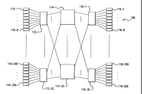
Fig. 1 illustrates a switch 100 consistent with an embodiment of the present
invention. Switch 100 includes a plurality of inputs 110-1 to 110-256, which
receive
signals conforming to a given protocol from an external network; group the
signals in
frames suitable for processing in switch 200; and forward the signals to a
first stage of
switch circuits 112-1 to 112-32. The data signals are routed through these
switch circuits
and passed to a second stage of switch circuits 114-1 to 114-22, which further
route the
data signals. A third stage of switch circuits direct the data to desired
outputs 118-1 to
118-256, which supply the data signals to an external network, but typically
in the
protocol in which the signals were input to switch 100.
Fig. 2 illustrates input 110-1 in greater detail. Remaining inputs 110-2 to
110-256
typically have a similar construction as input 110-1. Data is generally
supplied to input
110-1 as optical signals conforming to a Synchronous Optical Network (SONET)
protocol at a rate of approximately 2.5 Gbit/sec. A receiver circuit,
including for
example, photodetector 210 converts the received optical signals into
corresponding
electrical signals. A conventional clock and data recovery circuit 212
appropriately
shapes the electrical signals and extracts a clock signal for timing purposes.
A framer
circuit is coupled to the output of the clock and data recovery circuit, for
grouping the
received data into frames suitable for processing within switch 200.
As shown in Fig. 3, an exemplary frame 300 output from framer circuit 214
includes 18 time slots 301 to 318. The time slots are further grouped into
time division
multiplexed sub-frames 310, 320 and 330, having six time slots each. Each time
slot is
equivalent to an Synchronous Transport (STS) level 1 or STS-1 frame, and
transmits data
4
CA 02370800 2001-10-17
WO 01/31937 PCT/USOO/29614
at a rate of 54.84 Mbit/second.
The construction of switch circuit 112-1 will next be described with reference
to
Figs. 4(a), 4(b), 4(c), 5 and 6. Switch circuits 112-2 to 112-32 typically
have a similar
construction as switch circuit 112-1.
By way of introduction, switches can be classified into one of two categories,
space division and time division. Space division switches can be implemented
as
crossbar switches having m input and n outputs and mn crosspoints (m and n and
integers). By making an electrical contact via a crosspoint between a
horizontal input bus
and a vertical output bus, a connection can be made between the associated
input and
output, respectively.
Instead of using a space division switch, however, time division switching
techniques can also be applied for interconnecting inputs and outputs. A so-
called time
slot interchanger (TSI) can be used for such purposes. A TSI includes a buffer
which
reads from a single input and writes to a single output. The input is framed
into m fixed-
length time slots. The information in each input time slot is read
sequentially into
consecutive time slots (cyclically) of a buffer of m slots. The output is
framed into n time
slots, and information from the appropriate slot in the buffer is transmitted
on to a
corresponding output slot. Thus, over the duration of an output frame, the
content of the
buffer is read in predetermined manner according to a read-out sequence so
that the
information in each slot of the input frame is rearranged into the appropriate
slot in the
output frame. As a result, each time slot is interchanged.
Time division switching can be performed by a TSI. Since each time slot of a
multiplexed link is analogous to a circuit, the interchanging of information
in time slots is
comparable to switching of circuits in a space switch. Thus, a TSI can also be
used to
CA 02370800 2001-10-17
WO 01/31937 PCT/US00/29614
interconnect multiple input and outputs (each providing a single circuit),
provided that the
inputs are first multiplexed onto a single time division multiplexed (TDM)
stream, and
the time slot interchanged TDM stream from the TSI is then demultiplexed onto
the
outputs. The space-switched connections via a crossbar can therefore also be
realized by
a corresponding read-in sequence for time switched connections via a TSI.
Switching can
thus be achieved with either space division switches or time domain switches
with the
same result.
The present invention utilizes a combination of time division and space
switching
to logically create 2' center stage switching circuits in a switch
reconfigurable based on
the Looping Algorithm. The Looping Algorithm will next be described with
reference to
Figs. 4(a) to 4(c).
As seen in Fig. 4(a), the Looping Algorithm requires a switch having N inputs
and
N outputs, where N = 2 , n being an integer. In Fig. 4(b), switch 400 is
rearranged or
factored logically into N/2 sub-arrays 402 and 404, as well as 2 x 2 switch
stages 406 and
408. Further, in accordance with the Looping Algorithm, each 2 x 2 switch has
one
output coupled to upper sub-array 402 and one to lower sub-array 404 in Fig.
4(b). If
necessary, sub-arrays 402 and 404 can be further factored to yield additional
2 x 2 stages
as well as center stages including four N/4 sub-arrays.
An example of the steps carried out by the Looping Algorithm will next be
described with reference to Fig. 4(c). In a first step, an unconnected input
of 2 x 2 switch
420 in stage 406 is coupled, via upper switch 402, to desired output of 2 x 2
switch 422 in
stage 408. The adjacent output of switch 422 is then coupled to a desired
input, e.g., the
remaining input of switch 420, through lower switch 404. Another 2 x 2 switch
in stage
406 is then selected, connections are made through the upper switch 402 (loop
forward),
6
CA 02370800 2001-10-17
WO 01/31937 PCT/US00/29614
to an output of stage 408; and an adjacent output is coupled to an input of
stage 406
through lower switch 404 (loop back). This process is repeated until all
inputs are
coupled to corresponding outputs of switch 400.
Each of stages 112-1 to 112-32 is similarly logically factored into stages of
2 x 2
switches. However, in an example of the present invention, each of switch
circuits 112-1
to 112-32 is configured to receive and output 384 of the above-described time
slots. A
logical representation of switch circuit 112-1, for example, is shown in Fig.
5.
Switch 112-1 is a conventional cross-bar switch, configured to logically
include
stages of 2 x 2 switches 510, 512, 514, 516, 518, and 520 (see Fig. 5) after a
series of
factorizations as described above. After the factorizations are complete, the
stages are
rearranged so that the layout of the logical 2 x 2 switches is consistent with
the hardware
of the cross-bar switch. In particular, stage 510 is configured to have a bank
of switches
with 384 inputs receiving time slots on bus 522, and output two groups of time
slots on
192 byte-wide buses 524 and 526, respectively. Switch stage 512, includes two
banks
coupled to buses 524 and 526, and outputting data on 96 byte-wide buses 528 to
respective switch banks in stage 514. Each bank of switches in stage 514, in
turn, outputs
data onto 48 byte-wide buses 530, which are coupled to a respective one of
switch blocks
in stage 516. Each bank in stage 516 is coupled to a pair of 24 byte-wide
buses 532 for
supplying data to a corresponding one of switch banks in stage 518. As further
shown in
Fig. 5, switches in stage 518, receive data from respective ones of buses 532
and route the
data onto corresponding pairs of 12 byte-wide buses 536. The data is next
passed to
switch banks in stage 520, where it is routed onto 6 byte-wide busses, each of
which
being coupled directly to one of center stage switches 114-1 to 114-22.
Fig. 6 illustrates one of the switch banks shown in Fig. 5. Each bank includes
two
7
CA 02370800 2001-10-17
WO 01/31937 PCT/USOO/29614
sub-stages 620 and 630 have P 2 x 2 switches, where P is the width of the bus
coupled to
the inputs of each bank, e.g. P = 384 for the bank of stage 510, 192 for the
banks of stage
512, 96 for the banks of stage 514, 48 for the banks of stage 516, 24 for the
banks of stage
518, and 12 for the banks of stage 520. Connections between each of the 2 x 2
switches
are further illustrated in Fig. 6. These connections are consistent with the
requisite
hardware connections within each of switch circuits 112-1 to 112-32.
Returning to Fig. 5, each of switch banks 520 is logically coupled to a
respective
six byte wide bus, which carries one sub-frame having six time slots at any
given time. In
a physical implementation, however, three such buses are time division
multiplexed onto
a single line to obtain frames 300 discussed above with reference to Fig. 3.
As indicated
above, these frames further include three sub-frames, each of which including
six time
slots each. Each six byte wide output bus of switch banks 520 is next fed to a
respective
one of center stage switch circuits 114-1 to 114-22. Since the sub-frames are
effectively
time switched, which is equivalent to space switching, additional switches can
be
logically created in the center stage as discussed in detail below.
Fig. 7 illustrates connections to center stage switch circuits 114-1 to 114-22
in
greater detail. Switch circuit 114-1, for example, is coupled to a six-byte
wide output bus
from each of switch circuits 112-1 to 112-32. Since each bus carries three
time division
multiplexed sub-frames, each of center stage switches 114-1 to 114-221ogically
receives
an eighteen byte-wide bus from each of switch circuits 112-1 to 112-32 due to
the
equivalence of time and space switching. The sub-frames can be rearranged
within
switches 114-1 to 114-22 and regrouped into frames which are then supplied on
one of 32
output lines to a respective one of third stage switch circuits 116-1 to 116-
32.
In the particular example of the invention discussed herein, there are 384
outputs
8
CA 02370800 2001-10-17
WO 01/31937 PCT/USOO/29614
from each of switch circuits 112-1 to 112-32, and the outputs are grouped into
18 time
slots each. Thus, the minimum number of center stage switches is 22
(384/18=22). Since
this number is not a power of 2, the Looping Algorithm cannot be applied in a
conventional sense. However, consistent with the present invention, each of
center stage
switch circuits 114-1 to 114-22 is logically subdivided into three sub-
switches (shown in
phantom in Fig. 7 as blocks 701, 702, 703 to 764), each of which receiving a
respective
time division multiplexed sub frame of six time slots. In addition, the number
of logically
subdivided sub-switches can be equal to the number of sub-frames. Since there
are 22
physical center stage switches, there are a total of 3 x 22, i.e., 66, logical
center stage sub-
switches. In this instance, the Looping Algorithm only requires 64 ( 26=64)
center stages.
Accordingly, the Looping algorithm can be implemented even though there is not
a power
of 2 physical center stage switches. In addition, two of the logical stages
can be used as
spares 780.
Fig. 8 illustrates center stage switch circuit 114-1 in greater detail. Switch
circuit
114-1 may have a similar construction as remaining switch circuits 114-2 to
114-22.
Moreover, each of these switch circuits may be implemented with a crossbar
switch,
logically configured to include three sub-switches.
Frames from each of switch circuits 112-1 to 112-32 are supplied to a
respective
one of time division demultiplexers 810-10 to 810-32, which separate three sub-
frames
from each frame. The separated sub frames are supplied to a respective one of
sub-
switches 701, 702 and 703 for appropriate routing therethrough. Outputs from
each of
sub-switches 701 to 703 are coupled to a respective one of time division
multiplexers
830-1 to 830-32. Time division multiplexer 830-1, for example, receives sub-
frames
from each of switches 701 to 703, and combines these sub-frames to output a
frame to
9
CA 02370800 2001-10-17
WO 01/31937 PCT/USOO/29614
switch circuit 116-1. In a similar fashion, remaining time division
multiplexers output
frames to corresponding switch circuits 116-2 to 116-32 for further routing.
Switch circuits 116-1 to 116-32 are constructed in a similar fashion as switch
circuits 112-i to 112-32. Accordingly, these switches route data and are
reconfigurable
in the manner described above with reference to Figs. 4(a) - 4(c), 5 and 6.
Each of switch
circuits 116-1 to 116-32 supplies signals to respective groupings of outputs.
For example,
switch circuit 116-1 supplies frames to outputs 118-1 to 118-8, while switch
circuit 116-
32 is coupled to outputs 118-249 to 118-256.
In general, outputs 118-1 to 118-256 take received data, reframe the data to
its
original format and protocol when it was input to switch 100, and convert the
data to
optical signals for further transmission. Typically, the output optical
signals conform to
the same SONET protocol as optical signals input to switch 100.
Fig. 9 illustrates output 118-1 in greater detail. Output 118-1 includes
framer
circuit 910 coupled to receive data from an output port of switch 116-1.
Framer circuit
910 reframes the received data into a format in which the data was input to
switch 200.
The data, in the form of electrical signals is next supplied to a transmitter
circuit 950,
including, for example driver circuit 920, which modulates laser diode 930
accordingly to
output corresponding optical signals.
In summary, a switch having a non-power of 2 number of center stage switches
can be reconfigured according to the Looping Algorithm by logically dividing
each
physical stage switch to obtain 2 logical switches. Data is further time
division
multiplexed and routed based on the logical configuration of the physical
center stage
switches. As a result, a switch can be quickly reconfigured using the Looping
Algorithm,
even though it has fewer center stage physical switches, which consume less
power and
CA 02370800 2001-10-17
WO 01/31937 PCT/US00/29614
occupy less space.
Other embodiments will be apparent to those skilled in the art from
consideration
of the specification and practice of the invention disclosed herein. It is
intended that the
specification and examples be considered as exemplary only, with a true scope
and spirit
of the invention being indicated by the following claims.
11