Note: Descriptions are shown in the official language in which they were submitted.
CA 02370836 2001-10-18
WO 00/64666 PCT/US99/08861
O OPTICAL RECORDING MEDIA HAVING INCREASED ERASABILITY
FIELD OF THE INVENTION
The invention disclosed herein relates generally to optical
recording media and more specifically to optical recording media
having a recording layer comprising optical phase-change memory
materials.
BACKGROUND OF THE INVENTION
Non-ablative, optical phase-change data storage systems,
record information in an optical phase-change memory material
that is switchable between at least two detectable states by the
application of optical energy. Optical phase-change memory
material is typically incorporated in an optical recording medium
having a structure such that the optical phase-change memory
material is supported by a substrate and protected by
encapsulants. In the case of optical recording media, the
encapsulants include, for example, anti-ablation materials and
layers, thermal insulation materials and layers, anti-reflection
materials and layers, reflective layers, and chemical isolation
layers. Moreover, various layers may perform more than one of
these functions. For example, anti-reflection layers may also be
anti-ablation layers and thermal insulating layers. The
thicknesses of the layers, including the layer or layers of
optical phase-change memory material, are engineered to minimize
the energy necessary for effecting the state change as well as
to optimize the high contrast ratio, high carrier-to-noise ratio
and high stability of the optical phase-change memory materials.
Formation of optical recording media includes deposition of
the individual layers by, for example, evaporative deposition,
chemical vapor deposition, and/or plasma deposition. As used
herein plasma deposition includes sputtering, glow discharge, and
plasma assisted chemical vapor deposition.
An optical phase-change material is capable of being
switched from one detectable state to another detectable state
or states by the application of optical energy. The state of the
phase-change changeable material is detectable by properties such
1
CA 02370836 2001-10-18
WO 00/64666 PCT/US99/08861
as, for example, index of refraction, optical absorption, optical
reflectivity, or combinations thereof. Tellurium based materials
have been utilized as phase-change materials for data storage
where the change is evidenced by a change in a physical property
such as reflectivity. Tellurium based state changeable
materials, in general, are single or multi-phased systems. The
ordering phenomena of such materials includes a nucleation and
growth process (including both or either homogeneous and
heterogeneous nucleations) to convert a system of disordered
materials to a system of ordered and disordered materials. The
vitrification phenomena includes attaining a high mobility state
and rapid quenching of the phase changeable material to transform
a system of disordered and ordered materials to a system of
largely disordered materials. The above phase changes and
separations occur over relatively small distances, with intimate
interlocking of the phases and gross structural discrimination,
and may be highly sensitive to local variations in stoichiometry.
The instant invention provides for high speed transformation by
passing through a high mobility state. This high mobility state
allows for high speed transformation from one state of relative
order to another. The high mobility state does not specifically
correspond to the molten state, but more accurately corresponds
to a state of high system mobility.
Generally, a laser is used to supply the optical energy to
cause the phase transitions between amorphous and crystalline
states in an optical phase-change memory material. The amount
of energy applied to the memory material is a function of both
the power of the laser as well as the period of time that the
laser pulse is applied. The crystallization energy is defined
herein as the amout of energy per unit volume needed to
substantially re-crystallize an amorphous region of the memory
material. The crystallization energy is dependent upon many
factors, including the energy necessary for nucleation during the
crystallization process.
If the crystallization energy is too high, the memory
material requires exposure to either a higher power laser pulse
or a longer laser pulse in order to convert the material from the
2
CA 02370836 2001-10-18
WO 00/64666 PCT/US99/08861
amorphous to the crystalline states. It is desireable to be able
to control the crystallization energy of a phase-change memory
material via the addition of one or more modifier elements. It
is also desirable to increase the erasability of optical
recording media.
SUMMARY OF THE INVENTION
One object of the present invention is an optical storage
medium having reduced energy requirements. Still another object
of the present invention is an optical recording media having
increased erasability.
These and other objects of the invention are satisfied by
an optical recording medium comprising one or more recording
layers, at least one of the recording layers comprising an
optical phase-change memory material comprising: an optical
phase-change alloy; and at least one modifier element, added to
the phase-change alloy, that increases the erasability of the
optical recording medium by at least 3 dB.
These and other objects of the invention are also satisfied
by an optical data storage and retrieval system comprising: an
optical drive means with an optical head for reading, writing and
erasing optical data to an optical recording medium, the optical
recording meium comprising one or more recording layers, at least
one of the recording layers comprising optical phase-change
memory material comprising: an optical phase-change alloy; and
at least one modifier element, added to the optical phase-change
alloy, that increases the erasability of the recording medium by
at least 3 dB.
3O BRIEF DESCRIPTION OF THE DRAWINGS
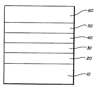
Figure 1 depicts a highly stylized view of a cross-section
of a multi-layered optical disk.
DETAILED DESCRIPTION OF THE INVENTION
Disclosed herein is an optical phase-change memory material
comprising an optical phase-change alloy, and at least one
modifier element which is added to the optical phase-change
3
CA 02370836 2001-10-18
WO 00/64666 PCT/US99/08861
alloy. Generally, the optical phase-change alloy of the present
invention may be any material that ( 1 ) has an amorphous state and
a crystalline state, (2) is capable of being switched between the
amorphous and crystalline states in response to optical energy,
and (3) undergoes a detectable change in either index of
refraction, optical absorption, or optical reflectivity when
switched between the amorphous and crystalline states. The
optical phase-change memory material of the present invention is
formed by modifying the above-mentioned phase-change alloy by
adding at least one modifier element to the optical phase-change
alloy to form a modified material. The phase-change alloy that
is modified by the addition of at least one modifier element to
form an optical phase-change memory material is referred to
herein as the "corresponding unmodified phase-change alloy".
As described, the optical phase-change memory material of
the present invention comprises an optical phase-change alloy,
and at least one modifier element which is added to the optical
phase-change alloy. Preferably, the modifier element, when added
to the optical phase-change alloy, decreases the crystallization
energy of the optical phase-change alloy by at least 50. More
preferably, the modifier element, when added to the optical
phase-change alloy, decreases the crystallization energy of the
optical phase-change alloy by at least 10%. In other words, the
optical phase-change memory material has a crystallization energy
which is preferably at least 5 0 lower, and more preferably at
least 100 lower, than the crystallization energy of the
corresponding phase-change alloy.
As defined herein, the "crystallization energy" is the
amount of energy per unit volume to substantially re-crystallize
an amorphized volume of phase-change material. The energy
needed to crystallize the volume of phase-change material may be
supplied by a laser beam pulse having power P and pulse width W.
The amount of energy E delivered to the amorphized volume is P
x W. The percentage difference in crystallization energy
between (1) the phase-change memory material of the present
invention and (2) the corresponding unmodified phase-change alloy
can be measured under "static" test conditions by irradiating
4
CA 02370836 2001-10-18
WO 00/64666 PCT/US99/08861
sample volumes of each (1) and (2) with a laser beam having power
P and pulse width W and measuring the optical reflectivities of
the samples.
As described above, the optical phase-change memory material
of the present invention comprises an optical phase-change alloy,
and at least one modifier element added to the phase-change
alloy. Disclosed herein is an optical recording medium
comprising one or more recording layers. At least one of the
recording layers comprises the optical phase-change memory
material described above (i.e., the optical phase-change memory
material comprises an optical phase-change alloy, and at least
one modifier element added to the phase-change alloy). In one
embodiment of the present invention, each of the recording layers
comprises the optical phase-change memory material described
above.
Preferably, the optical recording medium of the present
invention has an erasability which is at least 3 dB greater than
the erasability of an "unmodified" optical recording medium
(having the same structure) wherein each of the recording layers
is formed from the corresponding unmodified optical phase-change
alloy. More preferably, the optical recording medium of the
present invention has an erasability which is at least 5 dB
greater than the erasability of the unmodified optical recording
medium. Any optical recording medium having the characteristics
described above falls within the scope of the invention.
In one embodiment, the optical recording medium of the
present invention has one recording layer. The recording layer
is formed from the optical phase-change memory material of the
present invention (i.e., an optical phase-change alloy that has
been modified with the addition of at least one modifier
element). Preferably, this optical recording medium has an
erasability that is at least 3 dB greater than the erasability
of an "unmodified" optical recording medium (with the same
structure) wherein said recording layer is formed from the
corresponding unmodified phase-change alloy. More preferably,
the erasability of the optical recording medium is at least 5 dB
greater than the erasability of the unmodified optical recording
5
CA 02370836 2001-10-18
WO 00/64666 PCT/US99/08861
medium. Any optical recording medium having the characteristics
described above falls within the scope of the invention.
In another embodiment, the optical recording medium of the
present invention has two or more recording layers . At least one
of the optical recording layers comprises the optical memory
material described herein (i.e., an optical phase-change alloy
that has been modified with the addition of at least one modifier
element). Preferably, this optical recording medium has an
erasability that is at least 3 dB greater than the erasability
of an "unmodified" optical recording medium (with the same
structure) wherein each of the recording layers is formed from
the corresponding unmodified phase-change alloy. More
preferably, the erasability of the optical recording medium is
at least 5 dB greater than the erasability of the unmodified
optical recording medium. Any optical recording medium having
the characteristics described above falls within the scope of the
invention.
"Erasability" is defined herein as the difference between
the carrier-to-noise ratio of the recorded signal (the "record
CNR") and the carrier-to-noise ratio after erase (the "erase
CNR") of an optical recording medium (i.e., erasability = record
CNR - erase CNR). The record CNR is the ratio of the power of
a carrier frequency signal recorded onto the medium to the power
of the noise level of the medium. This is conventionally
expressed as: record CNR = 20*loglo(rms voltage of the recorded
signal/rms noise voltage). The erase CNR is the carrier-to-noise
ratio of the signal recorded into the medium after that portion
of the medium, where the signal was recorded, has been subjected
to an erase procedure.
The values of both the record CNR and the erase CNR vary
with the record power PW used. Hence, the erasability
measurements will also vary with the record power PW. As noted
above, the addition of the modifier element to the optical phase-
change alloy increases the erasability of the optical recording
medium by at least 3 dB. This 3 dB (or greater) increase will
occur at least at some record power Pw which is between the
"threshold power" Ptnresnoid and tre "ablation power" Pabitation
6
CA 02370836 2001-10-18
WO 00/64666 PCT/US99/08861
The threshold power Ptnresnold is defined herein as that power,
below which, there is no measureable record signal which can be
distinguished from the noise. The ablation power Pabiation is
defined herein as that power, above which, the material will
begin to ablate and become disfunctional. Preferably,
erasability measurements are made at an "optimal record power"
Popt. An example of an optical record power Popt at which the
erasability measurements may be made is the record power where
the second harmonic record CNR is minimized.
There are many examples of structures of optical recording
media. In one type of optical recording medium, the recording
layer is sandwiched between a first dielectric layer and a second
dielectric layer. In one embodiment of this type of optical
recording medium, the optical recording medium comprises at least
a substrate, a first dielectric layer deposited on top of the
substrate, a recording layer deposited on top of the first
dielectric layer, and a second dielectric layer deposited on top
of the recording layer. An example of a multi-layered optical
recording medium is shown in Figure 1. In this example, the
storage medium 1 includes a substrate 10, a first dielectric
layer 20 deposited on top of the substrate 10, a recording layer
deposited on top of the first dielectric layer 20, a second
dielectric layer 40 deposited on top of the recording layer, a
reflective layer 50 deposited on top of the second dielectric
25 layer 40, and a protective coating layer 60 deposited on top of
the second dielectric layer. The substrate 10 may be formed from
polycarbonate or other similar material. Preferably, the
substrate 10 is a substantially optically invariant,
substantially optically isotropic, transparent sheet. The
30 preferred thickness is between about 0.6mm to about 1.2 mm. The
substrate 10 is typically injection molded but can be formed by
other methods. Grooves may be placed in the substrate for
guiding the light delivered by a laser source. The grooves may
be polymerized, molded, injection molded or cast molded into the
substrate 10. Preferably, the thickness of the grooves may be
from about 200 to about 1000 Angstroms.
7
CA 02370836 2001-10-18
WO 00/64666 PCT/US99/08861
First and second dielectric layers 20, 40 sandwich the
recording layer 30. A primary function of the first and second
dielectric layers 20,40 is to optimize the reflectivity of the
optical source so as to maximize the amount of optical energy
delivered to the memory material from said source. Optimization
requires an appropriate choice for the "optical thickness" of the
first and second dielectric layers 20, 40. The optical thickness
of a layer of material is defined as the index of refraction of
the material multiplied by the physical thickness of the layer.
Preferably, the first and second dielectric layers are
chosen from a dielectric material having an optical index of
refraction between 1.5 and 2.5. More preferably, the optical
index of refraction is chosen between 2.0 and 2.2. Materials
which may be used for the first and second dielectric layers
include, but are not limited to, germanium oxide (Ge02), silicon
dioxide (Si02), zinc sulfide (ZnS), aluminum dioxide, titanium
oxide, and silicon nitride. The materials may be used
individually or in combination. One or both of the dielectric
layers 20, 40 may be layered or graded to avoid diffusion into
the recording layer 30.
As well as optimizing the reflectivity of the optical
source, the first and second dielectric layers 20, 40 provide a
means for thermally insulating the recording layer 30.
Moreover, they may also act to prevent agents which could
chemically change the memory material from penetrating the
recording layer 30. As well, they may also prevent the substrate
10 from deforming when the memory material is heated by the
optical source during recording or erasing.
A reflective layer 50 may be deposited on top of the second
dielectric layer 40. The reflective layer 50 increases the
quantity of reflected light entering the memory layer. It also
influences the thermal environment of the memory layer by
providing a thermal sink that encourages rapid cooling. In
general, the reflective layer is formed from a thin-film metal.
Preferred are high reflectance materials such as Al, Au, Ag, Pt,
Cu, Ti, Ni, Pd or alloys thereof. The reflective layer is
preferably about 30 to about 150 nm thick. The reflective layer
8
CA 02370836 2001-10-18
WO 00/64666 PCT/US99/08861
is preferably formed by physical deposition methods such as
sputtering and evaporation.
A protective layer 60 may be deposited on top of the
reflective layer 50 for the purpose of improving scratch and
corrosion resistance. It is preferably formed from organic
materials such as acrylates. More preferably, the protective
layer 60 is formed from radiation-curable compounds and
compositions which are cured by exposure to radiation (typically
electron radiation and ultraviolet radiation). The protective
layer 60 is preferably about 0.1 to about 15 micrometers thick.
It may be formed by any desirable one of conventional coating
methods including spin coating, gravure coating, or spray
coating.
In another example of a structure of an optical recording
medium, the optical recording medium may comprise at least a
substrate, a first protective layer, a recording layer, and a
second protective layer. Examples of this type of multi-layered
structure are described in U.S. Patent No. 5,063,097, the
disclosure of which is incorporated by reference herein. In
yet another example of a structure of an optical recording
medium, the recording medium may comprise at least a substrate,
a lower dielectric layer, a recording layer, a first upper
dielectric layer, and a second upper dielectric layer. This type
of multi-layered structure is described in U.S. Patent No.
5,498,507, the disclosure of which is incorporated by reference
herein. In still another example of a structure of an optica l
recording medium, the recording medium may comprise at least a
substrate, a first reflective layer, a first dielectric layer,
a recording layer, a second dielectric layer, and a second
reflective layer. The optical recording medium of the
present invention comprises one or more recording layers. The
optical recording medium of the present invention may have one
recording layer. The optical recording medium may have two
recording layers. The optical recording medium may have three
recording layers. The optical recording medium may have four
recording layers. The optical recording medium may have five
recording layers. The optical recording medium may have six
9
CA 02370836 2001-10-18
WO 00/64666 PCT/US99/08861
recording layers. The optical recording medium may have seven
recording layers. The optical recording medium may have eight
recording layers. The optical recording medium of the present
invention may have more than eight recording layers.
As defined above, the optical phase-change memory material
of the present invention comprises an optical phase-change alloy,
and at least one modifier element added to the phase-change
alloy. As described above, the optical phase-change alloy of the
present invention may be any material that (1) has an amorphous
state and a crystalline state, (2) is capable of being switched
between the amorphous and crystalline states in response to
optical energy, and (3) undergoes a detectable change in either
index of refraction, optical absorption, or optical reflectivity
when switched between the amorphous and crystalline states.
Preferably, the modifier element is selected from the group
consisting of V, Cr, Mn, Fe, Co, Mo, Ru, Rh, Ta, W, Re, Os, and
Ir. More preferably, the modifier element is selected from the
group consisting of Fe, Cr, and Mo. Most preferably, the
modifier element is Fe.
As defined herein, the "atomic percentage" of an element,
is the percentage of that element, per number of atoms, within
the optical phase-change memory material. In one embodiment, the
modifier element is added to the optical phase-change alloy so
that the atomic percentage of the modifier element is between
0.06 and 1Ø
When Fe is used as the modifier element, it is preferable
that the atomic percentage of Fe is between 0.06 and 1.0, it is
more preferable that the atomic percentage of Fe is between 0.08
and 0.8, it is most preferable that the atomic percentage is
about 0.3. In an alternate embodiment, the atomic percentage of
Fe may be about 0.1.
As defined above, the crystallization energy of a material
is the amount of energy per unit volume necessary to
substantially re-crystallize an amorphized volume of phase-change
material. Crystallization can be divided into two basic steps:
( 1 ) the formation of nuclei, and ( 2 ) the growth of said nuclei
into crystals. The nucleation process may be either homogeneous
CA 02370836 2001-10-18
WO 00/64666 PCT/US99/08861
nucleation or heterogeneous nucleation. Generally, the amount
of energy needed for heterogeneous nucleation is less than that
required for homogeneous nucleation. Though not wishing to be
bound by theory, it is believed that the modifier element adds
heterogeneous nucleation sites to the optical phase-change alloy.
The addition of heterogeneous nucleation sites reduces the amount
of energy necessary for nucleation and thereby reduces the
crystallization energy of the phase-change material. Further,
the decrease in crystallization energy of the phase-change
material increases the erasability of the optical recording
medium using the phase-change material. It is believed that at
atomic percentages below about 0.06, the modifier element does
not provide enough heterogeneous nucleation sites to favorably
affect the nucleation characteristics of the material, and at
atomic percentages that are above about 1.0, the modifier element
has no additional beneficial effect, and can in some cases
deleteriously affect the desirable characteristics of the phase-
change material.
In one embodiment of the present invention, the optical
phase-change alloy comprises Ge, Sb, and Te. This is defined
herein as a GeSbTe phase-change alloy. In one embodiment, the
ratio of Ge atoms to Sb atoms to Te atoms (i.e., Ge:Sb:Te) is
chosen as approximately 4:1:5 to form a "4:1:5 alloy".
Preferably, the optical phase-change alloy comprises Ge, Sb, Te
in the ratio GeWSbXTeY where 36~ws42, 7<_x<_13, and 48<_ys54. More
preferably, w+x+y=1000. The modifier element is added to the
GeSbTe phase-change alloy to form the optical phase-change memory
material of the present invention.
In another embodiment, the ratio of atoms Ge:Sb:Te is chosen
as approximately 1:2:4 to form a "1:2:4 alloy". Preferably, the
optical phase-change alloy comprises Ge, Sb, Te in the ratio
GeWSbXTey where 11<_wsl7, 25sx<_31, and 53<_y<_59. More preferably,
w+x+y=1000. The modifier element is added to the GeSbTe phase
change alloy to form the optical phase-change memory material of
the present invention.
In another embodiment, the ratio of atoms Ge:Sb:Te is chosen
as approximately 2:2:5 to form a "2:2:5 alloy". Preferably, the
11
CA 02370836 2001-10-18
WO 00/64666 PCT/L1S99/08861
optical phase-change alloy comprises Ge, Sb, Te in the ratio
GeWSbXTey where l9sws25, l9sxs25, and 53<_ys59. More preferably,
w+x+y=100%. The modifier element is added to the GeSbTe phase
change alloy to form the optical phase-change memory material of
the present invention.
The modifier element Fe may be added to the optical phase-
change alloy to form an optical phase-change memory material
comprising Ge, Sb, Te, and Fe. As discussed, the atomic
percentage of Fe is preferably between 0.06 and 1.0 percent, more
preferably between 0.08 and 0.8 percent, and most preferably
about 0.3 percent. Specific examples of the optical phase-change
memory material comprising the above-mentioned phase-change alloy
include, but are not limited to, (Ge39Sb1oTe51) 9g.7Fe0,3,
(GelqSb28Te56) 99.7Fe0.03~ (Ge22Sb22Te56) 99.7Fe0.3~
In another embodiment of the present invention optica l
phase-change alloy comprises Ge, Sb, Te, and Se. This is defined
herein as a GeSbTeSe phase-change alloy: As is discussed in U.S.
Patent No. 5,278,011, herein incorporated by reference, the
element Se may be used to slow the crystallization process of the
phase-change alloy thereby making it easier to form the amorphous
phase. The Se retards crystallite formation during the
vitrification process as the material forms its final structure
during relaxation from the high mobility state . Preferably, the
Se is substituted for the Te and is added to the phase-change
alloy so that it makes up about 5 to 15 atomic percent of the
resulting composition. More preferably, selenium is added so
that it makes up about 5 to 11 atomic percent of the composition.
Most preferably, selenium is added so that it makes up about 7
to 10 atomic percent of the composition. In one embodiment
selenium makes up about 7 atomic percent of the composition. In
another embodiment selenium makes up about 8 percent of the
composition. In yet another embodiment selenium makes up about
9 percent of the composition. In yet another embodiment,
selenium makes up about 10 percent of the composition.
Selenium retards the formation of crystallites in the
amorphous state. Compositions with concentrations of Se higher
than about 15 atomic percent have crystallization speeds that are
12
CA 02370836 2001-10-18
WO 00/64666 PCT/US99/08861
too low. Additionally, compositions with concentrations of Se
lower than about 5 atomic percent have higher crystallization
speeds that favor formation of the crystalline phase, thereby
requiring a higher power for amorphization.
In one embodiment of the present invention, the optical
phase-change alloy is formed by substituting between 5 and 11
atomic percent of Se for Te in the 4:1:5 alloy described above.
Hence, it is preferable that the phase-change alloy comprises Ge,
Sb, Te, and Se in the ratio GeWSbXTey_ZSeZ where 36<_w_<42, 7<_x<_13,
48<_y<_54, and 5szs11. More preferably, w+x+y+z=100%.
In another embodiment, between 5 and 11 atomic percent of
Se is substituted for Te in the 1:2:4 alloy described above. It
is preferable that the phase-change alloy comprises Ge, Sb, Te,
and Se in the ratio GeWSbxTey-ZSeZ where 11<_wsl7, 25<_x<_31,
53<_y<_59, and 5_<zsll. More preferably, w+x+y+z=1000.
In yet another embodiment, between 5 and 11 atomic percent
of Se is substituted for Te in the 2:2:5 alloy described above.
It is preferable that the phase-change alloy comprises Ge, Sb,
Te, and Se in the ratio GeWSbXTey-ZSez where 19<_w<_25, 19<_x<_25,
53<_ys59, and 5szs11. More preferably, w+x+y+z=1000.
The modifier element may be added to the GeSbTeSe phase-
change alloy. Specifically, Fe may be added to the above-
mentioned optical phase-change alloy to form an optical phase-
change memory material having a composition comprising Ge, Sb,
Te, Se, and Fe. Preferably, the atomic percentage of the Fe is
between 0.06 and 1Ø More preferably, the atomic percentage of
Fe is between 0.08 and 0.8. Most preferably, the atomic
percentage of Fe is about 0.3. In an alternate embodiment the
Fe may be added to the optical phase-change alloy so that the
atomic percentage of the Fe is about 0.1. Specific examples of
optical phase-change memory materials of the present invention
include, but are not limited to, (Ge3gSbloTeqqSe7) gg.7Feo.3,
(Ge22Sb22Teq7Seg) 99.7Fe0.3~ and (GelqSb28Teq7Seg) g9.7Fe0.3
Also disclosed herein is an optical data storage and
retrieval system. The optical data storage and retrieval system
comprises an optical drive means with an optical head for
reading, writing and erasing optical data to an optical recording
13
CA 02370836 2001-10-18
WO 00/64666 PCT/US99/08861
medium. The optical head may include a laser. The optical head
is used to store data to and erase data from the optical
recording medium. The recording medium has a recording layer
comprising the optical phase-change memory material that has been
disclosed above. The optical recording medium may be removable
or non-removable, and may be disposed in a protective cartridge
case or freestanding (i.e., not disposed in a protective case).
Example
Experiments have been performed on a disc structure having
a substrate, a first dielectric layer formed on the substrate,
a recording layer formed on the first dielectric layer, and a
second dielectric layer formed on the recording layer. The first
dielectric layer, recording layer, and second dielectric layer
have optical thicknesses equal to 1/4, 1/2, and 1/2 of the 780
nm wavelength of the laser beam used as the source of optical
energy. The first and second dielectric layers are formed from
a mixture of ZnS and Si02. The disc radius is 3.207cm, the disc
rotation rate is 29.8Hz, the disc linear velocity is 6m/s, the
record power is varied between 2 and 15 mW, the record frequency
is 4MHz, the pulse width is 100ns, the erase power is 5mW, the
read power is 1.499mW. Table 1 shows record CNR, erase CNR and
erasability (record CNR - erase CNR) versus record powers between
2 and 15 mW. The recording layer in Table 1 is formed from the
phase-change alloy having the composition Ge4oSb1oTe91Se9. Table
2 also shows record CNR, erase C/N and erasability (record CNR
erase CNR) versus record powers between 2 and 15 mW. In Table
2, the optical phase-change memory material is formed from the
phase-change alloy Ge4oSb1oTe41Se9 to which .3o Fe had been added.
(Hence, the composition is (Ge4oSb1oTe41Se9) 99.7Feo.3) . Table 3 is
a comparison of the erasabilities from Tables 2 and 3. Note
that, in this particular example, for record powers from 7 to 13
mW, the erasability of the recording medium having a recording
layer formed from an optical phase-change materal comprising the
optical phase-change alloy and . 3 0 of the modifier element Fe was
at least 3 dB greater than the erasability of the recording
medium formed from the alloy alone without the additional
14
CA 02370836 2001-10-18
WO 00/64666 PCT/US99/08861
modifier element. The record powers of 7 to 13 mW are above the
threshold power Ptnresnold and below the ablation power Pabiation as
defined above.
Table 1 - phase-change memory material Ge4oSbloTeQlSe9
is
Record Power mW record CNR erase CNR dB erasability dB
dB
2 10.3 9.0 1.3
3 10.1 9.9 0.2
4 10.4 9.0 1.4
5 9.0 9.0 0.0
6 31.0 18.5 12.5
7 36.2 24.6 11.6
8 37.9 19.0 18.9
9 39.6 21.5 18.1
10 41.2 24.5 16.7
11 40.7 28.7 12.0
12 42.8 30.7 12.1
13 42.2 33.3 8.9
14 42.5 35.3 7.2
15 43.2 35.6 7.6
Table 2 - phase-change memory material is
S b 1 o T a Q 1 S a 9 ~ 9 9 . 7 F a o . 3
Record Power mW record CNR dB erase erasability dB
CNR dB
2 10.8 8.5 2.3
3 8.6 10.1 -1.5
4 9.5 10.3 -0.8
5 10.5 9.3 1.2
6 19.2 9.5 9.7
7 26.0 9.2 16.8
8 31.4 9.2 22.2
9 35.0 9.3 25.7
10 35.8 11.5 24.3
11 35.6 15.2 20.4
12 36.5 20.3 16.2
13 36.4 22.5 13.9
14 3.6 2.9 0.7
15 2.5 2.4 0.1
CA 02370836 2001-10-18
WO 00/64666 PCT/US99/08861
Table 3 - erasability comparison
Record Power mW erasability(no Fe) erasability(with Fe)
change
2 1.2 2.3 1.1
3 0.2 -1.5 1.7
4 1.4 -0.8 2.2
5 0.0 1.2 1.2
6 12.5 9.7 2.8
7 11.6 16.8 5.2
8 18 . 9 22 . 2 3.3
9 18.1 25.7 7.6
10 16.7 24.3 7.6
11 12.0 20.4 8.4
12 12.1 16.2 4.1
13 8 . 9 13 . 9 5.0
14 7.2 0.7 ~.5
15 7.6 0.1 7.5
While the invention has been described in connection with
preferred embodiments and procedures, it is to be understood that
it is not intended to limit the invention to the described
embodiments and procedures. On the contrary it is intended to
cover all alternatives, modifications and equivalence which may
be included within the spirit and scope of the invention as
defined by the claims appended hereinafter.
16