Note: Descriptions are shown in the official language in which they were submitted.
CA 02371074 2001-10-22
-1-
KW228
SPECIFICATION
BS DIGITAL BROADCASTING RECEIVER
TECHN/CAL FIELD
[00011 The present invention relates to a BS digital broadcasting receiver for
receiving a BS digital signal wherein a signal modulated by a hierarchical
transmission system typically represented by a BS digital broadcasting
receiver
for receiving a BS digital TV broadcasting is time-division-multiplexed.
BACKGROUND ART
[0002] A BS digital broadcasting adopts a hierarchical modulation system and
a system called burst symbol insertion that allows reception at a low CNR. A
main signal is sent by frame and through time division multiplexing by using
one
or more modulation systems of 8PSK modulation, QPSK modulation and BPSK
modulation. A burst symbol (BS) and a TMCC signal are BPSK-modulated.
[0003] As publicly known, one frame in the hierarchical transmission system is
comprised of 39,936 symbols by inserting burst symbols (BS) among the TMCC
signals, 8PSK main signals, ... , QPSK main signals and the main signals as
shown in FIG. 11 A.
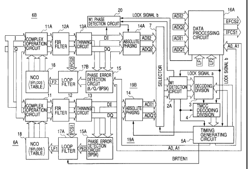
[0004] As shown in FIG. 12, a BS digital broadcasting receiver operates to
convert received signals into intermediate frequency signals, perform on a
complex operation circuit 11 a complex operation on I and Q signals acquired
by
orthogonally detecting the intermediate frequency signals by a
CA 02371074 2001-10-22
-2-
quasi-synchronous detection system so as to demodulate them, and pass them
through a roll-off filter 12 comprised of a FIR filter to convert them into
symbol
streams on a thinning circuit 13.
[0005] From demodulation data DI and DQ outputted from the thinning circuit
13, frame synchronization pattern detection, carrier regeneration, absolute
phasing and TMCC decoding are sequentially performed as mentioned later, and
a carrier regeneration phase error table according to a modulation system
based
on modulation system identifying signals comprised of A0 and Al signals for
the
sake of identifying sections of an 8PSK modulation wave, a QPSK modulation
wave and a BPSK modulation wave respectively is selected, and the
demodulation data DI and DQ are received and supplied to a phase error
detection circuit 15 constituting a phase comparator for detecting a phase
error,
from which circuit a phase error voltage required for carrier regeneration is
acquired and supplied to a loop filter 17 so as to acquire a tuning voltage.
[0006] The tuning voltage outputted from a loop filter 17 is supplied to a
numerical control frequency oscillator 18 from which data of sincot and data
of
cosc)t based on the tuning voltage is outputted from the numerical control
frequency oscillator 18 so as to perform the carrier regeneration. To be more
specific, the following complex operation is performed by using sincot and
coscwt,
namely the output of the numerical control frequency oscillator 18 and
orthogonal
detection output I and 0 so as to consequently acquire demodulation data DI
and
DQ.
DI cos It sin It I
DQ - -sinIt cosIt Q
CA 02371074 2001-10-22
3
[0007] The demodulation data DI and DQ are supplied to an absolute phasing
circuit 14 to be absolutely phased so as to match the phases to a sending end.
The absolutely phased demodulation data ADI and ADQ signals are supplied to a
W1 detection circuit 2 so as to detect a frame synchronization pattern (W1)
from
the demodulation data ADI and ADQ. The demodulation data for which frame
timing is established based on the frame synchronization pattern detected on
the
W1 detection circuit 2 is supplied to a decoder division 3 to be decoded.
[0008] If the frame timing is established by detecting the frame
synchronization pattern, time-series positions of the frame synchronization
pattern, TMCC signals, a super frame identification paitern and burst symbols
are
found respectively and decoded in a decoding division 3. The TMCC signals
outputted from the decoding division 3 are supplied to a TMCC decoding
division
to be decoded. A switching instruction signal based on the frame
synchronization pattern detected on the W1 detection circuit 2 and a receiving
CNR (when the CNR exceeds a predetermined value, it becomes "H") outputted
from the decoding division 3 and the decoded TMCC signals are supplied to a
tirning generating circuit 5 from which the modulation system identifying
signals
comprised of the A0 and Al signals and a burst enable signal (BRTEN)
indicating
that a carrier regeneration division will be a burst symbol division are sent.
[0009] The Al, A0, switching instruction and BRTEN signals are as shown in
FIG. 11 B, C, D and E. Moreover, in FIG. 12, a reference number 16 indicates a
data processing circuit performing an AFC action. And a phase error detection
circuit 15, the loop filter 17, the numerical control frequency oscillator 18
and the
CA 02371074 2001-10-22
-4-
data processing circuit 16 are combined to constitute a carrier regenerating
circuit 19 as a whole.
[0010] In the above conventional BS digital broadcasting receiver, one
demodulator circuit 1 is used so that, in receiving operation when the CNR is
high,
the carrier regeneration is performed by performing phase error detection
based
on all the modulation systems (continuous reception). In addition, in the
receiving operation when the CNR is low, the carrier regeneration is performed
by burst-receiving a BPSK-modulated signal (burst reception).
[0011] Burst reception can be implemented, if mentioned in detail, by
performing operation such as holding the output of the loop filter 17 on the
carrier
regenerating circuit 19. The BPSK-modulated signal is burst-received in the
receiving operation when the CNR is low, so that the carrier regeneration is
performed by using the phase error of the section.
[0012] However, there has been a problem that, in the case where performance
of a down converter of an outdoor unit (ODU) or the like including an antenna
is
insufficient, reception with little fixed deterioration is difficult when
performing the
burst reception compared with the continuous reception due to influence of its
phase noise.
[0013] For instance, if the BS digital broadcasting receiver receives the
8PSK,
QPSK and BPSK modulation waves at a high CNR, it performs the continuous
reception so as to implement the carrier regeneration. Here, if receiving
situation changes and the CNR lowers, it becomes difficult for the BS digital
broadcasting receiver to receive the 8PSK modulation wave and implement the
CA 02371074 2001-10-22
-5-
carrier regeneration so that it performs the burst reception to implement the
carrier regeneration except the 8PSK modulation section based on the switching
instruction signal (see FIG. 11D). A determination of the switching is made by
monitoring an error rate after trellis decoding and so on, and the switching
is set
on the BS digital broadcasting receiver so that it is switched at an arbitrary
value.
[0014] In the case of considering the carrier regeneration around the
switching
between a high CNR and an intermediate CNR, the marginal CNR when
performing the continuous reception is different from the marginal CNR when
performing the burst reception (see FIG. 3). This point will be described
based
on FIG. 13 hereafter.
[0015] FIG. 13 is a diagram of which horizontal axis is phase noise and
vertical axis is the marginal CNR, wherein (a) is the marginal CNR acquired
from
a bit error rate at 8PSK modulation reception when the carrier regeneration is
performed by the continuous reception, (b) is the marginal CNR acquired from a
bit error rate at 8PSK modulation reception when the carrier regeneration is
performed by the burst reception performed by the demodulation data of the
BPSK modulation section, (d) is the marginal CNR acquired from a bit error
rate
at QPSK modulation reception when the carrier regeneration is performed by the
continuous reception (except the 8PSK modulation section), (e) is the marginal
CNR acquired from a bit error rate at QPSK modulation reception when the
carrier regeneration is performed by the burst reception performed by the
demodulation data of the BPSK modulation section. Here, the marginal CNR is a
limit value wherein any CNR lower than it cannot be corrected in connected
sign
error correction.
CA 02371074 2001-10-22
-6-
[0016] For instance, when the phase noise 0 rms is 10 (deg), a switching
point from the continuous (BPSK, QPSK and 8PSK modulation sections)
reception to the burst reception is calculated at 9.5 dB (see FIG. 13 (a)) on
a shift
from high CNR reception to intermediate high CNR reception, and a switching
point from the burst reception to the continuous reception is calculated at 13
dB
(see FIG. 13 (b)) on a shift from the intermediate high CNR reception to the
high
CNR reception. Thus, there is hysteresis between mutual switching points of
the continuous reception and the burst reception (shown by an arrow (c) in
FIG.
13 for instance), and there further arises a problem that a factor of this
hysteresis
occurrence depends on the phase noise of the ODU. If phase noise
characteristics of the ODU are known in advance, technical countermeasures
can be taken, whereas it is actually impossible to predict the characteristics
since
the ODUs purchased by users are various. In order to solve this, it is also
thinkable to detect a degree of the ODU phase noise, which is by no means
easy.
[0017] In addition, when the phase noise 0 rms is 10 (deg) likewise for
instance, a switching point from the continuous (QPSK and 8PSK modulation
sections) reception to the burst reception is calculated at 3.5 dB (see FIG.
13 (d))
on a shift from low CNR reception to intermediate low CNR reception, and a
switching point from the burst reception to the continuous reception is
calculated
at 4 dB (see FIG. 13 (e)) on a shift from the intermediate low CNR reception
to
the low CNR reception. Thus, there is hysteresis between mutual switching
points of the continuous reception and the burst reception (shown by an arrow
(f)
in FIG. 13 for instance), and there further arises the same problem that the
factor
of this hysteresis occurrence depends on the phase noise of the ODU.
CA 02371074 2001-10-22
-7-
[0018] An object of the present invention is to resolve the problems in the
system of switching receiving methods and avoid the problem of uncertainty of
the switching point depending on the ODU phase noise so as to provide the BS
digital broadcasting receiver capable of optimum reception.
DISCLOSURE OF THE INVENTION
[0019] In order to attain the above object, the BS digital broadcasting
receiver
of the present invention for time-division-multiplexing a plurality of
poliphase PSK
modulation waves having different numbers of phases and receiving a digital
signal has first demodulation means having a first carrier regenerating
apparatus
for regenerating a carrier for demodulation based on a phase error in
demodulation data of a section of PSK modulation waves having the smallest
number of phases out of a plurality of poliphase PSK modulation waves, second
demodulation means having a second carrier regenerating apparatus for
regenerating a carrier for demodulation based on a phase error in demodulation
data of PSK modulation waves of the entire number of phases of a plurality of
poliphase PSK modulation waves, determination means for determining whether
or not each carrier regenerated by the first and second regenerating
apparatuses
is locked, and selector means for selecting and outputting either the
demodulation data outputted from the first demodulation means or the
demodulation data outputted from the first demodulation means.
[0020] And when it is determined by the determination means that the lock of
the carrier regenerated by the first carrier regenerating apparatus is
maintained
and the lock of the carrier regenerated by the second carrier regenerating
apparatus is in a locked state, the selector means operates to select the
demodulation data of the section of the PSK modulation waves having relatively
CA 02371074 2001-10-22
_8_
many phases outputted from the second demodulation means and select the
demodulation data of the section of the PSK modulation waves having relatively
few phases outputted from the first demodulation means so as to output the
data.
[0021] Moreover, the plurality of poliphase PSK modulation waves of the
present invention are typically comprised of the BPSK, QPSK and 8PSK
modulation waves.
[00221 A first embodiment of the present invention further has CNR operation
means for, when the carrier regenerated by the first carrier regenerating
apparatus is in a locked state, acquiring a CNR from distribution of receiving
points of the demodulation data outputted from the first demodulation means,
and
the first carrier regenerating apparatus operates to regenerate the carrier
for
,demodulation based on the phase error in demodulation data of a BPSK
modulation section, and the second carrier regenerating apparatus operates, in
the case where the CNR is the first predetermined value or more, to regenerate
the carrier for demodulation based on the phase errors in demodulation data of
the BPSK modulation section, the QPSK modulation section and the 8PSK
modulation section, and the selector means operates, in the case where the CNR
acquired by operation is the second predetermined value or more, to select the
demodulation data of the 8PSK modulation section outputted from the second
demodulation means and select the demodulation data of the BPSK modulation
section and the QPSK modulation section outputted from the first demodulation
means so as to output the data.
[0023] In a second embodiment, the first carrier regenerating apparatus
operates to regenerate the carrier for demodulation based on the phase error
in
CA 02371074 2001-10-22
_9_
the demodulation data of the BPSK modulation section, and the second carrier
regenerating apparatus operates, in the case where the CNR is less than the
first
predetermined value, to regenerate the carrier fnr demodulation based on the
phase errors in demodulation data of the BPSK modulation section and the
QPSK modulation section, and the selector means operates, in the case where
the CNR acquired by the operation is less than the second predetermined value,
to select the demodulation data of the QPSK modulation section outputted from
the second demodulation means and select the demodulation data of the BPSK
modulation section outputted from the first demodulation means so as to output
the data.
[0024j In a third embodiment, the first carrier regenerating apparatus
operates
to regenerate the carrier for demodulation based on the phase error in the
demodulation data of the BPSK modulation section, and the second carrier
regenerating apparatus operates, in the case where the CNR is the first
predetermined value or more, to regenerate the carrier for demodulation based
on the phase errors in the demodulation data of the BPSK modulation section,
the QPSK modulation section and the 8PSK modulation section, and also in the
case where the CNR is less than the first predetermined value, to regenerate
the
carrier for demodulation based on the phase errors in demodulation data of the
BPSK modulation section and the QPSK modulation section, and the selector
means operates, in the case where the CNR acquired by the operation is the
second predetermined value or more, to select the demodulation data of the
8PSK modulation section outputted from the second demodulation means and
select the demodulation data of the BPSK modulation section and the QPSK
modulation section outputted from the first demodulation means, and in the
case
where the CNR acquired by the operation is less than the predetermined second
CA 02371074 2001-10-22
- 10 -
value, to select the demodulation data of the QPSK modulation section
outputted
from the second demodulation means and select the demodulation data of the
BPSK modulation section outputted from the first demodulation means so as to
output the data.
[0025] Each of the above embodiments has copy means for, in the case
where the carrier regenerated by the second carrier regenerating apparatus is
not locked, copying the output from the loop filter in the first carrier
regenerating
apparatus when the carrier regenerated by the first carrier regenerating
apparatus is in a locked state to the output from the loop filter in the
second
carrier regenerating apparatus.
[0026] Furthermore, the determination means preferably outputs a lock signal
for representing that the regenerated carrier of each demodulation means
entered a lock range, based on the demodulation data from the first and second
demodulation means and the modulation system identifying signals.
BRIEF DESCRIPTION OF THE DRAWINGS
[0027] FIG. 1 is a block diagram showing a configuration of a BS digital
broadcasting receiver related to an embodiment of the present invention.
[0028] FIG. 2 is a block diagram showing a configuration of a data processing
circuit of the BS digital broadcasting receiver related to an embodiment of
the
present invention.
[0029] FIG. 3 is a flowchart for explaining workings of the BS digital
broadcasting receiver related to an embodiment of the present invention.
CA 02371074 2001-10-22
[0030] FIG. 4 is a flowchart for explaining workings of the BS digital
broadcasting receiver related to an embodiment of the present invention.
[0031] FIG. 5 is a block diagram showing another configuration of the data
processing circuit of the BS digital broadcasting receiver related to an
embodiment of the present invention.
[0032] FIG. 6 is a block diagram showing a configuration of a deformation
example of the BS digital broadcasting receiver related to an embodiment of
the
present invention.
[0033] FIG. 7 is a block diagram showing a configuration of a data processing
circuit of a deformation example of the BS digital broadcasting receiver
related to
an embodiment of the present invention.
[0034] FIG. 8 is a flowchart for explaining workings of a deformation example
of the BS digital broadcasting receiver related to an embodiment of the
present
invention.
[0035] FIG. 9 is a flowchart for explaining workings of a deformation example
of the BS digital broadcasting receiver related to an embodiment of the
present
invention.
[0036] FIG. 10 is a flowchart for explaining workings of a deformation example
of the BS digital broadcasting receiver related to an embodiment of the
present
invention.
CA 02371074 2001-10-22
- 12 -
[0037] FIG. 11 is a timing chart for switching receiving modes in the BS
digital
broadcasting receiver related to an embodiment of the present invention and a
deformation example thereof.
[0038] FIG. 12 is a block diagram showing a configuration of a conventional
BS digital broadcasting receiver.
[0039] FIG. 13 is a drawing explaining a marginal CNR by phase noise in
continuous reception and burst reception.
BEST MODE FOR CARRYING OUT THE INVENTION
[0040] Hereafter, a BS digital broadcasting receiver related to the present
invention will be described by an embodiment thereof.
[0041] FIG. 1 is. a block diagram showing a configuration of a BS digital
broadcasting receiver related to an embodiment of the present invention. The
BS digital broadcasting receiver related to an embodiment of the present
invention has two demodulator circuits. In addition, FIG. 1 shows the same
symbols as to the same components as those of a conventional BS digital
broadcasting receiver shown in FIG. 12.
[0042] The BS digital broadcasting receiver related to an embodiment of the
present invention has demodulator circuits 6A and 6B. The demodulator circuit
6A has a phase error detection circuit 15A having a phase error table for
detecting a phase error signal only from demodulation data of a BPSK
modulation wave (also referred to as the demodulation data of a BPSK
modulation section, and likewise in the case of other modulation) instead of a
CA 02371074 2001-10-22
- 13 -
phase error detection circuit 15 in a demodulator circuit 1 in the
conventional BS
digital broadcasting receiver. The demodulator circuit 6B further has a W1
phase detection circuit 20 in a demodulator circuit 1.
[0043] The BS digital broadcasting receiver related to an embodiment of the
present invention has a selector 7 for selecting either demodulation data ADI1
and ADQ1 outputted from the demodulator circuit 6A or demodulation data ADI2
and ADQ2 outputted from the demodulator circuit 6B, a W1 detection circuit 2A
for having the demodulation data selected by the selector 7 and a lock signal
a
supplied, a decoding division 3, a TMCC decoding division 4, a timing
generation
circuit 5A for having TMCC signals, a frame synchronization pattern and a lock
signal b supplied, and a data processing circuit 16A. The phase error
detection
circuit 15A, a loop filter 17A and a numerical control frequency oscillator 18
constitute a carrier regenerating circuit 19A, and the phase error detection
circuit
15, a loop filter 17B and a numerical control frequency oscillator 18
constitute a
carrier regenerating circuit 19B.
[0044] The demodulator circuit 6A is a main demodulator circuit and performs
on a complex operation circuit 11 a complex operation on I and Q signals
orthogonally detected by a quasi-synchronous detection system with output from
the numerical control frequency oscillator 18, and supplies demodulation data
DI
and DQ outputted through a roll-off filter 12 and a thinning circuit 13 to the
phase
error detection circuit 15A for performing carrier regeneration from the
demodulation data of the BPSK modulation section to acquire a phase error
voltage PED required for carrier regeneration and supplies it to the loop
filter 17A,
where a tuning voltage LF1 is acquired. The tuning voltage LF1 outputted from
the loop filter 17A is supplied to the numerical control frequency oscillator
18, and
CA 02371074 2001-10-22
- 14 -
the I and Q signals are demodulated by performing a complex operation for
phase rotation based on an oscillation frequency from the numerical control
frequency oscillator 18. This demodulation is performed by the regenerated
carrier based on the demodulation data of the BPSK modulation wave.
[0045] The selector 7 initially selects the demodulation data ADI1 and ADQ1
outputted from the demodulator circuit 6A. The W1 detection circuit 2A detects
the frame synchronization pattern (W1) from the demodulation data ADI1 and
ADQ1, and if frame timing is established, time-series positions of the frame
synchronization pattern, TMCC signals super frame identification pattern and
burst symbols are found respectively so that a burst enable 1 (BRTEN1) signal
shown in FIG. 11F is outputted from the timing generation circuit 5A.
[0046] A lock signal a is received, and the TMCC signals are decoded in a
decoding division 4.
[0047] The phase error detected by the phase error detection circuit 15A is
supplied to the loop filter 17A, and filtering/holding operation is performed
on the
BRTEN1 signal outputted from the timing generation circuit 5A. On the phase
error detection circuit 15A, however, only a phase error table for the
demodulation data of the BPSK modulation section is provided, so that carrier
regeneration based on the phase error acquired from for the demodulation data
of the BPSK modulation section is performed on the a carrier regenerating
circuit
19A. This regenerated carrier allows burst reception, and low CNR reception
becomes possible by performing reception of only the BPSK modulation section
(burst reception).
CA 02371074 2001-10-22
- 15 -
[0048] Various modulation signals including the above signal of the
BPSK-modulated section are absolutely positioned on a sending end so that it
is
possible to restore an absolute phase on a receiving end from a standard of a
receiving point of the frame synchronization pattern. In the burst reception
operation of the BPSK modulation section, it is received either in an absolute
phase or in a 180-degree rotated phase. As for determination of which phase it
was received in, the frame synchronization pattern W1 that is
"11101100110100101000" if received in the absolute phase just becomes
"0001 001 1 001 01 1 01 01 1 1 " in an opposite phase so that absolute phasing
can be
performed by a detected phase of the frame synchronization pattern.
[0049] The timing generation circuit 5A outputs all the modulation system
identifying signals (A0 and Al) that recognize the 8PSK, QPSK and BPSK
modulation system sections in a transmission mode out of the TMCC signals
decoded by the TMCC decoding division 4.
[0050] The demodulator circuit 6B performs on a complex operation circuit
11 A a complex operation on I and Q signals orthogonally detected by a
quasi-synchronous detection system with output from the numerical control
frequency oscillator 18A, and supplies demodulation data DI and DQ outputted
through a roll-off filter 12A and a thinning circuit 13A to the phase error
detection
circuit 15A for performing carrier regeneration from the demodulation data of
the
BPSK modulation section, the QPSK modulation section and 8BSK modulation
section to acquire the phase error voltage required for carrier regeneration
and
supplies it to the loop filter 17B, where a tuning voltage LF2 is acquired.
CA 02371074 2001-10-22
- 16 -
[0051] The tuning voltage LF2 outputted from the loop filter 17B is supplied
to
the numerical control frequency oscillator 18A, and the I and Q signals are
demodulated by performing a complex operation based on the oscillation
frequency from the numerical control frequency oscillator 18A. In this phase
error detection, based on the demodulation system identification number, the
phase error tables for the demodulation data of the BPSK modulation section,
the
QPSK modulation section and the 8PSK modulation section are switched so as
to detect a phase error and perform the carrier regeneration for each of them.
Absolute phasing is performed based on the results of detecting a reception
phase of the frame synchronization pattern W1 and receiving the lock signal b
in
the W1 phase detection circuit 20.
[0052] As described above, the demodulator circuit 6B basically performs the
carrier regeneration by implementing the continuous reception. The selector 7
selects the demodulation data AD12 and ADQ2 outputted from the demodulator
circuit 6B in the 8PSK modulation section after establishing synchronization
based on the lock signal b, and selects in other sections the demodulation
data
AD11 and ADQ1 outputted from the demodulator circuit 6A.
[0053] The BS digital broadcasting receiver related to an embodiment of the
present invention does not perform switching control of the continuous
reception
and the burst reception in high CNR reception and intermediate CNR reception.
[0054] Operation of the data processing circuit 16A is basically AFC operation
of the carrier regeneration of the demodulator circuit 6A, carrier lock
determination of the demodulator circuits 6A and 6B and control of the loop
filters
17A and 17B of the demodulator circuits 6A and 6B.
CA 02371074 2001-10-22
- 11 -
[0055] The data processing circuit 16A is configured as shown in FIG. 2,
where it detects by a carrier regeneration and synchronization detecting
circuit
161 that the regenerated carrier is locked (in this specification, to be
locked
means that the regenerated carrier has entered a lock range of the carrier
regenerating circuit) from the demodulation data ADI2 and ADQ2 and the
modulation system identifying signals (A0 and Al) and outputs the lock signal
b,
and likewise detects by a carrier regeneration and synchronization detecting
circuit 162 that the regenerated carrier is locked from the demodulation data
ADI1 and ADQ1 and the modulation system identifying signals and outputs the
lock signal a, and performs an operation on an error frequency by an error
frequency operation circuit 163 from the demodulation data ADI1 and ADQ1 and
the modulation system identifying signals, and outputs a control voltage IFCS1
to
the loop filter 17A by a control circuit 164 from the lock signal a, the lock
signal b,
the tuning voltages LF1 and LF2 and the error frequency signal, and then
outputs
a control voltage EFCS2 to the loop filter 17B.
[0056] Operation of the data processing circuit 16A will be mainly described.
First of all, frame synchronization is performed on the W1 detection circuit
2A by
rough scanning operation (a scan value is given from the control voltage IFCS1
to the tuning voltages LF1) of the AFC. At this time, the regenerated carrier
is
not locked on the demodulator circuit 6A yet. It calculates the error
frequency of
the regenerated carrier from the signals of the TMCC section of the
demodulation
data ADI1 and ADQ1 knowable from the demodulation system identifying signals
(AO and Al), and superimposes the error frequency on the tuning voltage LF1 so
as to set the tuning voltages LF1 by way of the control voltage IFCS1.
CA 02371074 2001-10-22
- 18 -
[0057] Thereafter, it burst-operates the loop filter a 7A. Burst operation
controls the loop filter 17A with BRTEN1 as an enable signal, and renders the
TMCC signal section and the burst symbol section as its enable sections. It
checks the lock of the regenerated carrier by detecting distribution of the
receiving points of the demodulation data ADI1 and ADQ1 in the TMCC signal
section and the burst symbol section knowable from demodulation system
identifying signals (A0 and Al).
[0058] When it is detected from the lock signal a that the regenerated carrier
is
locked, all the receiving points are absolutely phased by an absolute phasing
circuit 14, and the TMCC signals are decoded at the TMCC decoding division 4.
The decoded TMCC signals are received and the modulation system identifying
signals A0 and Al are generated at the timing generation circuit 5A. The
tuning
voltage LF1 of the demodulator circuit 6A is copied to the tuning voltage LF2
by
way of the control voltage EFCS2.
[0059] If it is checked with the lock signal b that the regenerated carrier in
the
demodulator circuit 6B is locked in the same manner as the above demodulator
circuit 6A, all the receiving points of the demodulation data DI and DQ
outputted
from the demodulator circuit 6B are absolutely phased. And then, the selector
7
selects the demodulation data AD12 and ADQ2 in the 8PSK modulation section
from the demodulator circuit 6B and the demodulation data of other modulation
sections from the demodulator circuit 6A. The selector 7 selects the
demodulation data from the demodulator circuit 6A in an initial state and when
the regenerated carrier of the demodulator circuit 6B is unlocked.
CA 02371074 2001-10-22
- 19 -
[0060] In addition, as for the above method of checking the lock, there is a
method, for instance, of calculating distribution values of the receiving
points
based on the demodulation data of BPSK-modulated burst symbols.
[0061] As described above, the data processing circuit 16A checks the lock of
the regenerated carrier and then provides the tuning voltage LF1 as the
control
voltage EFCS2 of the demodulator circuit 6B, and monitors AD12 and ADQ2 to
check the lock of the carrier regeneration. Moreover, in the case of the
intermediate CNR reception and the low CNR reception, it is highly likely that
the
regenerated carrier of the demodulator circuit 6B is not locked, and so the
value
of the tuning voltage LF2 may remarkably slump.
[0062] In that case, however, the data processing circuit 16A copies the
tuning
voltage LF1 to the tuning voltage LF2 by controlling the control voltage EFCS2
every time it is unlocked so that the tuning voltage LF2 will not be far from
the
tuning voltage LF1, in other words, so that it will stay within a capture
range of
the demodulator circuit 6B. Accordingly, the turiing voltage LF2 recovers
fast,
and besides, the burst reception and the continuous reception are
simultaneously
performed, and so it is possible to avoid the problem of uncertainty of the
mode
switching level depending on the ODU phase noise.
[0063] Moreover, a deformation example of the data processing circuit 16A will
be described. FIG. 5 is a block diagram of the data processing circuit 16B
that
is a deformation example of the data processing circuit 16A. The data
processing circuit 16B provides an error frequency operation circuit 163A
instead
of the error frequency operation circuit 163 in the data processing circuit
16A,
and the error frequency is computed by the error frequency operation circuit
CA 02371074 2001-10-22
- 20 -
163A from the modulation system identifying signals AO and Al and a phase
error signal PED outputted from the phase error detection circuit 15A.
Otherwise, it is the same as the data processing circuit 16A.
[0064] Next, the above workings in the BS digital broadcasting receiver
related
to an embodiment of the present invention will be described according to the
flowcharts shown in FIGS. 3 and 4.
[0065] If a channel is selected (step Si), the W1 frame is synchronized from
the demodulation data AD11 and ADQ1 (step S2). Following the step S2, timing
signals of the TMCC signal section and the burst symbol section are generated
(step S3). In the step S3, the TMCC signals, the burst symbols and the
modulation system identifying signals (A0 and Al) for indicating the BPSK
modulation section are generated. Following the step S3, the AFC action of
the demodulator circuit 6A is performed (step S4), and carrier regeneration by
the
TMCC signals and the burst symbols is performed on the demodulator circuit 6A
(step S5). In the step S5, only the BPSK modulation section is received by the
BRTEN1 signal.
[0066] Following the step S5, it is checked whether or not the regenerated
carrier is locked on the demodulator circuit 6A, and when it is determined as
unlocked, it is repeatedly executed again from the step S2 following the step
S6
until getting locked. When the regenerated carrier is determined to be locked,
absolute phasing is performed following the step S6 (step S7), and then the
TMCC signals are decoded (step S8). Following the step S8, the timing signals
of the modulation system identifying signals A0 and Al for identifying all the
CA 02371074 2001-10-22
- 21 -
modulation systems are sent (step S9), and the tuning voltage LF1 of the
demodulator circuit 6A is copied to the tuning voltage LF2 (step S10).
[0067] Following the step S10, it is checked whether or not the lock of the
regenerated carrier of the demodulator circuit 6A is maintained (step S11),
and
when it is determined that the lock thereof is not maintained, it is
repeatedly
executed again from the step S2 following the step S11. When it is determined
that the lock of the regenerated carrier is maintained in the step S11, it is
checked following the step S11 whether or not the regenerated carrier of the
demodulator circuit 6B is locked (step S12).
[0068] When it is determined that the lock of the regenerated carrier is not
maintained in the step S12, the demodulation data ADI1 and ADQ1 outputted
from the demodulator circuit 6A is selected by the selector 7 following the
step
S12 (step S13), and then it is executed again from the step S10.
[0069] In the step S 12, when it is determined that the lock of the
regenerated
carrier is maintained, absolute phasing is performed on the demodulation data
D12 and DQ2 by the W1 phase detection circuit 20 foilowing the step S12 (step
S14), and then the demodulation data ADI2 and ADQ2 of the 8PSK modulation
section of the demodulator circuit 6B is selected by the selector 7, and other
demodulation data of the QPSK and BPSK sections is selected from the
demodulation data ADI1 and ADQ1 from the demodulator circuit 6A (step S15),
and it is repeatedly executed from the step S11.
[0070] As described above, according to the BS digital broadcasting receiver
related to an embodiment of the present invention, the demodulator circuit 6B
CA 02371074 2001-10-22
- 22 -
constantly performs continuous reception irrespective of the high CNR
reception
or the intermediate CNR reception, and so a bit error rate (BER) of the 8PSK
modulation section will not be influenced by the ODU phase noise. On the other
hand, as the demodulator circuit (6A) constantly performs burst reception of
BPSK-modulated waves irrespective of the high CNR reception or the
intermediate CNR reception, the carrier regeneration will not break down and
the
frame synchronization will not fail. Accordingly, it is not necessary to make
a
difficult determination of where to select the optimum point for switching the
above described high CNR reception and intermediate CNR reception, and there
is little influence from the phase noise. In addition, the control of
switching itself
is not required so that the operation becomes stable.
[0071 ] Next, a deformation example of the BS digital broadcasting receiver
related to an embodiment of the present invention will be described.
[0072] FIG. 6 is a block diagram showing a configuration of a deformation
example of the BS digital broadcasting receiver related to an embodiment of
the
present invention. This deformation example is a case that allows switching
from
the high CNR reception to the intermediate high CNR reception and also
switching from the intermediate CNR reception to,the low CNR reception.
[0073] In this deformation example, the demodulator circuit 6A has the same
configuration as that of the BS digital broadcasting receiver related to an
embodiment of the present invention. FIG. 6 shows a BRTEN2 signal that is the
same signal as the BRTEN1 signal. As shown in FIG. 11 G, a demodulator
circuit 6C is different in that, instead of the loop filter 17B on the
demodulator
circuit 6B, it uses a carrier regenerating circuit 19C having a loop filter
17C
CA 02371074 2001-10-22
- 23 -
wherein a BRTEN3 signal is supplied for enabling the BPSK modulation section,
the QPSK modulation section and 8BSK modulation section on the high CNR
reception or the intermediate high CNR reception and enabling the BPSK
modulation section and the QPSK modulation section on the intermediate low
CNR reception or the low CNR reception.
[0074] Furthermore, this deformation example is different from the BS digital
broadcasting receiver related to an embodiment of the present invention in
that,
as shown in FIG. 7, instead of the data processing circuit 16B, a data
processing
circuit 16C is used, wherein a CNR calculation circuit 165 for acquiring the
CNR
from the distribution values of the receiving points comprised of the
demodulation
data ADI1 and ADQ1 is added to the data processing circuit 16B, and that,
instead of the timing generation circuit 5A, a timing generating circuit 5B is
used,
wherein the CNR acquired from the above distribution values is supplied.
[0075] Next, the workings of this deformation example will be described
centering on the operation of the data processirig circuit 16C. First of all,
the
frame synchronization is performed on the W1 detection circuit 2A by rough
scanning operation (a scan value is given from the control voltage IFCS1 to
the
tuning voltage LF1) of the AFC. At this time, the regenerated carrier is not
locked on the demodulator circuit 6A yet. It calculates the error frequency of
the
regenerated carrier from the signals of the TMCC section of the demodulation
data ADI1 and ADQ1, and superimposes the error frequency on the tuning
voltage LF1 so as to set the tuning voltages LF1 by way of the control voltage
IFCS1.
' CA 02371074 2001-10-22
- 24 -
[0076] Thereafter, it burst-operates the loop filter 17A. Burst operation
controls the loop filter 17A with BRTEN2 as an enable signal, and renders the
TMCC signal section and the burst symbol section as its enable sections. It
checks the lock of the regenerated carrier by detecting distribution of the
receiving points of the demodulation data AD11 and ADQ1 in the TMCC signal
section and the burst symbol section.
[0077] When the regenerated carrier is locked, all the receiving points are
absolutely phased by the absolute phasing circuit 14, and the TMCC signals are
decoded at the TMCC decoding division 4. The distribution values of the
receiving points are calculated from the demodulation data ADI1 and ADQ1 so as
to acquire the CNR. If the CNR is an intermediate high or higher CNR, the
decoded TMCC signals are received and the modulation system identifying
signals A0 and Al are generated at the timing generation circuit 5B, and the
modulation system identifying signal BRTEN3 is rendered as high potential.
The tuning voltage LF1 of the demodulator circuit 6A is copied to the tuning
voltage LF2 by way of the control voltage EFCS2.
[0078] If it is checked that the regenerated carrier in the demodulator
circuit
6C is locked in the same manner as the above demodulator circuit 6A, all the
receiving points of the demodulation data DI and DQ outputted from the
demodulator circuit 6C are absolutely phased. And then, the selector 7 selects
the demodulation data ADI2 and ADQ2 in the 8PSK modulation section from the
demodulator circuit 6C and the demodulation data of other modulation sections
from the demodulator circuit 6A.
CA 02371074 2001-10-22
- 25 -
[0079] On the other hand, if the CNR is not intermediate high or higher, the
TMCC signals are decoded and the modulation system identifying signals A0 and
Al are generated at the timing generation circuit 5B, and the BRTEN3 signal is
rendered as low potential only in the 8PSK modulation section, that is,
disabled
therein only and rendered as high potential in other modulation sections. The
tuning voltage LF1 of the demodulator circuit 6A is copied to the tuning
voltage
LF2 of the demodulator circuit 6C by way of the control voltage EFCS2.
[0080] If it is checked that the regenerated carrier of the demodulator
circuit
6C is locked, the receiving points based on the demodulation data ADI2 and
ADQ2 of the demodulator circuit 6C are absolutely phased. And then, the
selector 7 selects the demodulation data of the QPSK modulation section from
the demodulator circuit 6C and the demodulation data of other modulation
sections from the demodulator circuit 6A. The selector 7 selects the
demodulation data from the demodulator circuit 6A in an initial state and when
the regenerated carrier of the demodulator circuit 6C is unlocked.
[0081] Next, the above workings in the deformation example of the BS digital
broadcasting receiver related to an embodiment of the present invention will
be
described according to the flowcharts shown in FIG. 8 to FIG. 10.
[0081] If a channel is selected (step S21), the W1 frame is synchronized from
the demodulation data ADI1 and ADQ1 (step S22). Following the step S22, the
timing signals of the TMCC signal section and the burst symbol section are
generated (step S23). In the step S23, the modulation identifying signals (A0
and Al) for identifying the BPSK modulation section signals are generated.
Following the step S23, the AFC action of the demodulator circuit 6A is
CA 02371074 2001-10-22
- 26 -
performed (step S24), and carrier regeneration by the TMCC signals and the
burst symbols is performed on the demodulator circuit 6A (step S25). In the
step S5, only the BPSK modulation section is received by the BRTEN2 signal.
[0083] Following the step S25, it is checked whether or not the regenerated
carrier is locked on the demodulator circuit 6A, and when it is determined as
unlocked, it is repeatedly executed again from the step S22 following the step
S26 until getting locked. When the regenerated carrier is determined to be
locked, absolute phasing is performed foilowing the step S26 (step S27), and
then the TMCC signals are decoded (step S28). Following the step S28, the
timing signals of the modulation system identifying signals AO and Al for
identifying all the modulation systems are sent (step S29), and it is checked
whether the CNR is an intermediate high or higher CNR (step S30).
[0084] In the step S30, if the CNR is determined to be an intermediate high or
higher CNR, the modulation system identifying signals A0 and Al are generated
and the BRTEN3 is constantly rendered as high potential (step S31), and the
tuning voltage LF1 of the demodulator circuit 6A is copied to the tuning
voltage
LF2 of the demodulator circuit 6C (step S32). Following the step S32, it is
checked whether or not the lock of the regenerated carrier of the demodulator
circuit 6A is maintained (step S33).
[0085] When it is determined that the lock of the regenerated carrier of the
demodulator circuit 6A is not maintained in the step S33, the step S22 is
executed from the step S33. When it is determined that the lock of the
regenerated carrier of the demodulator circuit 6A is maintained in the step
S33, it
is checked following the step S33 whether or not the regenerated carrier of
the
CA 02371074 2001-10-22
- 27 -
demodulator circuit 6C is locked (step S34). When it is determined that the
regenerated carrier of the demodulator circuit 6C is not locked in the step
S34,
the demodulation data of the demodulator circuit 6A is selected by the
selector 7
and the step S30 is executed (step S35).
[0086] In the step S4, when it is determined that the lock of the regenerated
carrier of the demodulator circuit 6C is locked, absolute phasing is performed
on
the demodulation data D12 and DQ2 by the W1 phase detection circuit 20 (step
S36), and then the demodulation data ADI2 and ADQ2 of the 8PSK modulation
section of the demodulator circuit 6C is selected by the selector 7, and other
demodulation data of the QPSK and BPSK sections is selected from the
demodulator circuit 6A (step S37), and it is checked whether or not the CNR is
an
intermediate high or higher CNR (step S38), and if the CNR is determined to be
an intermediate high or higher CNR, it is repeatedly executed from the step
S33.
[0087] When the CNR is not determined to be intermediate high or higher in
the step S38, or when the CNR is not determined to be intermediate high or
higher in the step S30, the modulation system identifying signals A0 and Al
are
generated, and the BRTEN3 signal is rendered as low potential only in the 8PSK
modulation section (step S39). Following the step S39, the tuning voltage LF1
of
the demodulator circuit 6A is copied to the tuning voltage LF2 of the
demodulator
circuit 6C (step S40).
[0088] Following the step S40, it is checked whether or not the lock of the
regenerated carrier of the demodulator circuit 6A is maintained (step S41).
When it is determined that the lock of the regenerated carrier of the
demodulator
circuit 6A is not maintained in the step S41, it is repeatedly executed from
the
CA 02371074 2001-10-22
- 28 -
step S22 following the step S41. When it is determined that the lock of the
regenerated carrier of the demodulator circuit 6A is maintained in the step
S41, it
is checked whether or not the regenerated carrier of the demodulator circuit
6C is
locked (step S42).
[0089] When it is determined that the lock of the regenerated carrier of the
demodulator circuit 6C is not locked in the step S42, it is repeatedly
executed
from the step S35. When it is determined that the lock of the regenerated
carrier of the demodulator circuit 6C is maintained in the step S42, absolute
phasing is performed on the demodulation data D12 and DQ2 by the W1 phase
detection circuit 20 following the step S42 (step S43), and then the
demodulation
data ADI2 and ADQ2 of the QPSK modulation section of the demodulator circuit
6C are selected by the selector 7, and other demodulation data of the 8PSK and
BPSK sections are selected from the demodulator circuit 6A (step S44).
[0090] Following the step S44, it is checked whether or not the CNR is a high
CNR or an intermediate high CNR (step S45), and if the CNR is determined not
to be a high CNR or an intermediate high CNR in the step S45, it is repeatedly
executed from the step S41, and if the CNR is determined to be a high CNR or
an intermediate high CNR in the step S45, it is repeatedly executed from the
step
S30.
[00911 To be more specific, in this deformation example, the BRTEN3 signal is
always the high potential in the high CNR and the intermediate high CNR
reception, and becomes the low potential only in the 8PSK modulation section
in
the intermediate low CNR and the low CNR reception. In the high CNR and the
intermediate high CNR reception, the BRTEN2 signal is the low potential during
CA 02371074 2001-10-22
- 29 -
the QPSK modulation section and 8BSK modulation section, and the
demodulator circuit 6A is performing burst reception of the BPSK modulation
section.
[0092] In the low CNR reception, the demodulator circuit 6A performs burst
reception only in the BPSK modulation section while the BRTEN2 signal
becomes the high potential. The roles of the demodulator circuit 6A are to
maintain basic synchronization of the carrier regeneration system under the
high
CNR and the intermediate high CNR reception, to regenerate data of the QPSK
modulation section, and to maintain basic synchronization of the carrier
regeneration system under the intermediate low CNR and the low CNR reception.
The roles of the demodulator circuit 6C are to regenerate data of the 8PSK
modulation section in the carrier regeneration by the continuous reception
under
the high CNR reception, and to regenerate data of the QPSK modulation section
and the BPSK modulation section by the burst reception except the 8PSK
modulation section under the intermediate low CNR reception.
[0093] The respective determinations of the high, intermediate high,
intermediate low and low CNR reception can be made by a circuit for computing
the CNR (in the data processing circuit 16). In particular, on a determination
of
the intermediate high or intermediate low CNR, the receiving mode of the
demodulator circuit 6A is switched to the demodulator circuit 6B, and
selection of
the selector 7 is switched to the data regeneration system by the demodulator
circuit 6B. By doing so, the demodulator circuit 6B constantly performs burst
reception except the 8PSK modulation section irrespective of the intermediate
low CNR reception or the low CNR reception, and so the BER of the QPSK
modulation section will not be influenced by the ODU phase noise.
CA 02371074 2001-10-22
- 30 -
[0094] On the other hand, as the demodulator circuit 6A constantly performs
burst reception only in the burst symbol section irrespective of the
intermediate
low CNR reception or the low CNR reception, the carrier regeneration will not
break down and the frame synchronization will not fail. Accordingly, it is
possible to avoid a difficult problem of where to select the optimum point for
switching the intermediate low CNR because the other demodulator circuit 6C is
performing optimum reception, and there is little influence from the phase
noise.
In addition, the control of switching itself is not required so that the
operation
becomes stable.
INDUSTRIAL APPLICABILITY
[0095] As described above, the BS digital broadcasting receiver of the present
invention can avoid, by placing the demodulator circuits in parallel, the
problem of
uncertainty of the switching point depending on the phase noise due to
switching
of the receiving modes for the high CNR reception and the intermediate CNR
reception so as to allow optimum reception.