Note: Descriptions are shown in the official language in which they were submitted.
WO 00/69074 CA 02371083 2001-11-07 PCT/NZ00/00071
NESTED MODULATOR ARRANGEMENT
FIELD OF THE INVENTION
This invention relates to modulator arrangements and particularly but not
solely to
sigma-delta arrangements for radio frequency synthesisers which use fractional
division. More particularly the invention relates to nested modulator
arrangements
with global feedback. Nested arrangements can be used to modulate the
fractional
division process in a way which is substantially different from traditional
processes.
BACKGROUND TO THE INVENTION
Radio communication devices employ frequency synthesisers to control
transmission and reception of signals. A synthesiser generally includes a
reference
oscillator which generates a stable reference frequency signal and is used to
determine the output of a frequency controlled oscillator which in turn
generates a
variable RF output signal. This output signal is generally coupled to an
antenna of
the communication device by way of one or more mixers which modulate or
demodulate the signal for transmission or reception respectively. The
synthesiser
is programmed by a control unit such as a digital processor to produce the
controlled
oscillator signal at a range of frequencies as required by the device.
Most frequency synthesisers use one or more phase locked loops to generate the
variable output signal from the frequency controlled oscillator. The phase
locked
loop contains a phase discriminator which generates an output according to the
phase difference between the reference signal and a feedback signal. The
feedback
signal is generally produced by dividing the frequency of the output from the
controlled oscillator. Output from the phase discriminator is applied to a
loop filter
WO 00/69074 CA 02371083 2001-11-07 PCT/NZ00/00071
2
which provides a control signal for the controlled oscillator. Voltage rather
than
current controlled oscillators are normally used. In general terms, a feedback
loop
of this kind attempts to match the frequency of the controlled oscillator to a
multiple
of the reference frequency and stabilise with a zero phase difference between
the
reference and feedback signals.
Frequency division of the output from the frequency controlled oscillator can
be
implemented in various ways to enable a relatively low frequency reference to
determine a wide range of variable RF output. Fractional-N techniques are
commonly used and allow the synthesiser to achieve arbitrarily fine frequency
resolution. These techniques modulate the instantaneous integer divide ratio
of the
feedback to the phase discriminator to produce average non-integer division
ratios.
However, limit cycles in the modulation signal cause cyclic variation of the
division
value and generally produce spurious frequencies and additional phase noise in
the
synthesised output signal. Various cancellation schemes such as phase
interpolation
have been employed to reduce the fractional spurs and noise but generally
require
an increase in complexity and cost of the synthesiser to achieve significant
reduction
in the amplitude of the spurs.
Fractional-N synthesisers which use sigma-delta modulation to reduce phase
noise
and spurs resulting from non-integer division values are well known. A
conventional modulator formed by a cascade of modulators is described in US
4,609,881 for example. The sigma-delta technique arose as a development in
analog-to-digital conversion and has since been widely used in electronic
communication devices for a range of purposes. It involves feedback to improve
the
effective resolution of a coarse quantiser and allows shaping of the noise
which
arises from quantisation. In general terms, input is fed to the quantiser via
an
integrator with the quantised output being fed back and subtracted from the
input.
WO 00/69074 CA 02371083 2001-11-07 pCT/NZ00/00071
3
The output of the modulator therefore contains the original signal plus the
first
difference of the quantisation error. A detailed discussion of sigma-delta
techniques
can be found in Delta-Signaa Data Converters, IEEE Press 1997.
Higher order sigma-delta modulators generally use two or more integrators each
receiving feedback from the output to improve the overall noise performance. A
cascade is also sometimes used whereby the output of two or more modulators is
combined in a way which cancels the noise that they individually produce. In a
cascade of two first order modulators for example, output from the integrator
of the
first modulator is fed to the second modulator. The output of the second is
differentiated and subtracted from the output of the first to provide a
resultant signal.
This leaves the noise as the second difference of the quantisation error of
the second
modulator, in a form similar to that of a second order modulator. Multi-level
quantisers have also been used to improve the stability of higher order and
cascaded
modulators.
SUMMARY OF THE INVENTION
It is an object of the present invention to provide for improved or at least
alternative
modulator arrangements which may be used in frequency synthesisers. In general
these improvements are enabled by a nested modulator having logic control in a
global feedback stage. At least one of the nested elements will also
preferably
include logic control stages.
Accordingly in one aspect the invention may broadly be said to consist in a
nested
modulator arrangement comprising: first and second digital modulation stages
having respective inputs and outputs, the outputs of the modulation stages
being
combined to form a common output producing a resultant modulation signal, the
CA 02371083 2001-11-07 PCT/NZ00/00071
Received 28 March 2001
4
input of the first stage receiving a signal formed by combination of an
external
control signal with a feedback signal derived from the resultant modulation
signal,
and the input of the second stage receiving an internal control signal from
the first
stage.
In a second aspect the invention may be said to consist in a cascaded
modulator
arrangement comprising: two or more modulators each having an output coupled
to
a common combination stage which produces a resultant output, wherein a first
modulator receives an external control signal and subsequent modulators are
coupled in series to the first modulator so that each receives a control
signal from a
preceding modulator, and at least one of the modulators is a nested modulator
as set
out above.
BRIEF DESCRIPTION OF DRAWINGS
Preferred embodiments of the invention will be described with respect to the
drawings, of which:
Figure 1 shows a conventional accumulator acting as a first order sigma-delta
modulator which might be used in a frequency synthesiser,
Figure 2 shows a three-stage sigma-delta modulator formed by a cascade of
modulators such as shown in Figure l,
Figure 3 is an accumulator circuit with logic stages forming an improved first
order sigma-delta modulator,
AMENDED ~E~
~F'EA/AU
WO 00/69074 CA 02371083 2001-11-07 PCT/NZ00/00071
Figures 4a, 4b are second and third order modulators formed by a nested
arrangement of lower order modulators with global feedback,
Figure 5 is an embodiment of the second order nested modulator in Figure 4a
based on the modulator of Figure 3,
5 Figure 6 is a table showing how a global feedback logic stage can be
implemented in the modulator of Figure 5,
Figures 7a, 7b show alternative three stage modulators each formed by a
cascade including a second order nested modulator,
Figures 8a, 8b respectively show plots of spectral density for comparison of
the performance of a two stage cascade with the second order modulator of
Figure
5, and
Figures 9a, 9b respectively show sample output from the multi-stage
modulator systems of Figures 2, 7a.
DETAILED DESCRIPTION OF PREFERRED EMBODIMENTS
Refernng to these drawings it will be appreciated that modulators according to
the
invention may be constructed in various ways within the scope of the claims.
The
preferred embodiments are described by way of example only, and are not
limited
to use in frequency synthesisers. The known components of synthesisers and
modulator devices will be understood by a skilled person and a detailed
explanation
of their function need not be given.
Figure 1 shows a simple modulator 10 previously used in control of fractional-
N
division processes in frequency synthesisers. A controller varies the
instantaneous
value of N by way of the modulator to create a range of non-integer division
values
in the feedback path of the phase locked loop. In this example the modulator
involves a K-bit adder 11 which receives a control word k from the controller
as an
WO 00/69074 CA 02371083 2001-11-07 PCT/NZ00/00071
6
input on line 13. A latch 12 holds the current contents c of the adder as
another
input on line 14. Each clock pulse on line 15 causes the control word to be
added
to the contents of the adder. If the contents exceed 2K then an overflow
signal is
generated on line 16 and causes division by N+1 rather than N. For a constant
input
word the adder will overflow on every 2~/k clock pulses and produce a signal
which
represents two-level quantisation of the signal c. The output of the
synthesiser is
then anon-integer multiple ofthe reference frequency and the average division
value
in the feedback path is N + 2K/k. An accumulator overflow arrangement of this
kind
functions only approximately as an ideal first order sigma delta modulator.
Figure 2 shows a three stage modulator 20 formed by a conventional cascade of
first
order modulators 21, 22, 23 such as shown in Figure 1. In this example a
control
word X on line 24 produces a relatively complex signal Y which may be provided
to create non-integer division values in the frequency synthesiser. The
contents of
each accumulator forms an error signal which is provided as an input to the
next
stage, if any. The overflows of the accumulators can be filtered in various
ways to
achieve cancellation of successive error signals and reduce phase offsets in
the phase
locked loop. This leaves only high order error terms in the overall output Y.
A
conventional selection based on Pascal's triangle is shown. The filtering is
based
on a sum ~ (1- z~') °z -~M~°~'~yn, where yn is the output of the
nth stage, n = 0,1,2, M
is the number of stages and z -' represents a unit delay. Expansion of the
coefficient
of each term in the sum produces successive rows of Pascal's triangle. In
practice
this can be achieved by passing the overflow output of each accumulator
through a
pair ofrespective delay elements 25 and selecting signals a, b, c at
appropriate points
for input to a combination stage 26. Each modulator and each delay is clocked
by
the output of the divider in the phase locked loop.
WO 00/69074 CA 02371083 2001-11-07 PCT/NZ00/00071
7
Figure 3 shows a modulator 30 recently developed by the applicant for use in a
range
of systems such as frequency synthesisers. The contents of PCT/NZ00/207 are
incorporated herein by reference. An n-bit adder 31 has two inputs one of
which
receives a control word X. The second input receives an error signal a derived
from
output of the adder after various preferred feedback processes applied to
groups of
the most and least significant bits. An output logic stage 32 receives a group
of t
msbs from the adder and operates on the bits during a quantisation process
which
produces the modulator output Y. A feedback logic stage 33 also receives the
group
t from adder 31 and operates on the bits in a feedback process which
determines
overload and stability performance of the modulator. An m-bit adder 34
receives a
group of m msbs from the n-bit adder 31 and a group of m bits output by the
feedback logic stage 33. A latch 35 receives a group of n-m lsbs from the n-
bit
adder and a group of m bits from the m-bit adder to form the error signal. The
latch
receives a clock signal which moves the modulator from one state to the next
through addition processes in each of the adders. The output and feedback
logic
stages may be provided in various ways, such as a dedicated Boolean operation
or
a multiplexer. Required parameters may be set in hardware or held in
registers, for
example.
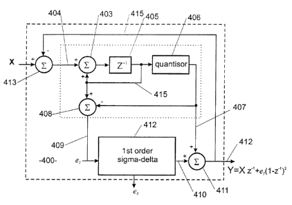
Figure 4a schematically shows a preferred modulator 400 having a nested
arrangement according to the invention. In this example a second order
modulator
is formed by linking a first order modulator 401 to another modulator 402, in
an
arrangement which can be extended to create still higher order systems.
Modulator
401 includes an addition element 403 which receives input on line 404, delay
element 405, quantisor 406 which produces output on line 407, and an addition
element 408 which produces an error signal on line 409. Addition and delay
elements 403 and 405 form an accumulator with output fed back on line 415.
Modulator 402 receives the error signal as input and produces output on line
410.
WO 00/69074 CA 02371083 2001-11-07 PCT/NZ00/00071
8
The individual outputs on lines 407 and 410 are combined in an addition
element
411 to form an output signal Y on line 412. An adder 413 at the input of the
modulator system combines a control word X with feedback on line 415 derived
from signal Y. In general, the input to each modulator stage is summed only
once
within the particular stage. The resultant output of the arrangement is that
signal Y
contains only second and higher order error terms.
Figure 4b shows a third order modulator 450 formed by linking a first order
modulator 451 with a second order modulator 452 such as that in Figure 4a. The
l0 arrangement shown is similar but not identical to that of Figure 4a. Delay
element
405 in the accumulator formed by addition element 403 and delay 405 is now
placed
in the feedback line 415, and an additional delay element 420 has been
included in
the output line 407. Output signal Y now contains only third and higher order
error
terms. In general an nth order system of this kind can be created by nesting
an
l5 (n-1)th order system. Each stage or level in the system is preferably
formed by an
ideal or at least approximate sigma-delta modulator linked to a modulator at a
lower
level stage , if any. The resultant output is generally a combination of the
individual
outputs produced at each level. Input to the modulator at each level is
derived from
an error signal output by the modulator at the next highest level. Input to
the system
?0 at the highest level is derived from combination of an external control
word with
feedback from the resultant output. Feedback of this kind may be termed
"global"
and preferably includes a logic stage.
Figure 5 shows a second order modulator 500 based on the system 400 of Figure
4
?5 and the modulator 30 in Figure 3. The top level modulator 502 is formed by
an n-bit
adder 503, latch 504, an output logic stage 505, feedback logic 506 and an
adder
507, which have been generally described in relation to Figure 3. The logic
stages
operate in accord with selectable coefficients which may be implemented as
WO 00/69074 CA 02371083 2001-11-07 PCT/NZ00/00071
9
previously described. Output from the top level modulator is provided on line
508
by the logic stage 505. A dither signal d may be combined as an input to the
feedback logic stage 506 to reduce the likelihood of cyclical patterns. The
dither
signal is typically a random or pseudo random sequence and is preferably pre-
y filtered by a transformation (1-z') to avoid a noise floor. An n-bit error
signal is
produced on line 509 by a combination of lsbs from latch 504 and msbs from
adder
507. The second level modulator 501 receives the error signal and produces an
output on line 510. The individual modulator outputs are combined in an m-bit
adder 511 to form the resultant output signal Y on line 512. An adder 513
combines
an m-bit control word X with feedback derived from the output signal Y. Adder
503
of the top level modulator forms an accumulator arrangement with latch 504 and
also receives an n-bit inputs from a combination of the control word X and
output
from the adder 513. Global feedback on line 515 involves a logic stage 516
which
operates according to a set of selectable coefficients to produce a signal on
line 520.
Figure 6 is a table outlining a possible selection of coefficients for the
logic stage
516 in Figure 5. In this example m=2 and the modulators 501, 502 produce
simple
bi-level outputs corresponding to binary values {0,1 } on lines 508, 510.
These map
to decimal values {-l, 1}. Adder 511 produces a 2-bit output having values
{0,1,2}which are fed back through logic stage 516. Adder 513 might be omitted
in
this arrangement depending on the range of fractional division values which
are
required.
Figures 7a, 7b respectively show three stage modulators 700, 750 formed by
cascades including a second order modulator according to the invention. In
each
case an input control word X produces a relatively complex signal Y which may
be
used to create non-integer division values in a fractional-N frequency
synthesiser.
An error signal output by each stage is provided as an input to the next
stage. The
WO 00/69074 CA 02371083 2001-11-07 PCT/NZ00/00071
outputs of the stages are combined in ways which contain higher order
corrections
for quantisation errors and thereby reduce phase offsets in the phase locked
loop of
the synthesiser. Low order error terms may thereby be cancelled in ways which
do
not necessarily involve the successive rows of a Pascal's triangle arrangement
shown
5 in Figure 2.
In Figure 7a the three stage modulator 700 comprises a second order stage 701
such
as that shown in Figure 5 followed by a first order stage 702. The stages may
well
have different input requirements and produce output and error signals of
different
10 bit lengths. Additional logic stages may be required, such as a scaling
function 703
which matches the error signal from stage 701 with the input of stage 702. In
this
example the output of stage 702 is passed through two delay elements 705 and a
selection of the output signal and corresponding delayed signals is combined
with
the output of stage 701 in a combining stage 706. The control word X produces
a
resultant output signal Y having third order error terms as shown.
In Figure 7b the three stage modulator 750 comprises a first order stage 751
followed by a second stage 752 such as shown in Figure 5. Again the stages may
have different input and output characteristics, typically due to the
modulators
including different quantisation functions, and additional logic such as a
scaling
function 753 may be required. In this example the output of each stage is
passed
through respective delay element 755 and a simple selection from the outputs
and
their corresponding delayed signals is made in the combining stage 756. Again
the
control word X produces a resultant output signal Y having only high order
error
terms and may be used as an alternative modulation signal for fractional-N
division
in a frequency synthesiser.
WO 00/69074 CA 02371083 2001-11-07 PCT/NZ00/00071
11
Figures 8a, 8b are respective plots of pokier spectral density (PSD) in the
output of
a cascaded modulator formed by two overflow accumulator stages, such as shown
in Figure l, and a second order nested modulator such as that shown in Figure
5.
Plots with spurs have been generated by deliberate operation of the modulator
systems in a limit cycle. The amplitudes of the spurs in Figure 8b are
significantly
less than those of Figure 8a.
Figures 9a, 9b are output samples for the modulator arrangements in Figures 2,
7a
respectively. Rows I, II, III in Figure 9a represent output from each of the
first order
stages 21, 22, 23 respectively before input to the delay elements 25. Row IV
represents output from the combination stage 26 as signal Y. Rows I, II, III
in
Figure 9b represent output from the first stage 502 in Figure 5, and from the
first and
second order stages 701 and 702 in Figure 7a. Row IV represents output from
the
combination stage 706. A limit cycle still appears in each output, although in
Figure
9b the spurious frequencies which result in the eventual output of the
frequency
synthesiser are reduced by the relatively active nature of the variations in
the signal
in Row IV.
Modulator arrangements according to the invention can be used in a variety of
electronic systems other than frequency synthesisers. In analog-to-digital
conversion for example. Various nested and cascade arrangements are possible
and
those which have been described are given by way of example only.