Note: Descriptions are shown in the official language in which they were submitted.
CA 02371527 2001-11-19
WO 00/70920 PCT/IE00/00067
"An Electronic Ballast Circuit"
Introduction
The present invention relates to an electronic ballast circuit for gas
discharge lamps
and in particular, but not exclusively for public security or amenity
applications.
Electronic ballast circuits have been developed to provide a steady voltage to
drive
gas discharge lamps or the like. However, due to the fact that the lamp is
being
driven at high frequencies they suffer from a number of problems, unstable
arc, poor
crest factor, and high frequency acoustic harmonics which may develop in the
circuit,
all of which considerably reduces the lifetime of the lamp and the quality of
the light
output. Commercially available ballasts use a fairly simple way to drive a
lamp by
high frequency load current through an inductor. Many in the industry are
aware of
the problems but heretofore there does not appear to have been any
commercially
available product that fully resolves this problem.
An example of such an electronic ballast is that described in PCT Patent
Application
No. WO 95/22194. This ballast utilises a square wave voltage waveform to drive
a
lamp. Such a square waveform sometimes called a driver waveform is recognised
as
being a particularly suitable waveform for gas discharge lamps. However, it is
suggested that this ballast would not solve the above problems in particular
by
providing a stable arc for lamp operation and preventing high frequency
acoustic
harmonics.
The high frequency pulsing of a lamp is inclined to produce an unstable arc in
the
circuit. The arc characteristics can vary every time you switch the lamp on
and off
again and this happens for every AC cross-over, but at high frequency, this
can
happen as many as 20,000 times a second and this has a detrimental affect on
the
arc stability. The arc intensity can oscillate and it also has the affect of
reducing
the lamp lifetime.
High frequency arc resonance is a problem accepted in the industry. It is
believed
that having these high frequency resonances can also cause the metal welds to
CA 02371527 2001-11-19
WO 00/70920 PCT/IE00/00067
- 2 -
vibrate within the lamp, thus physical structure fatigue will occur at the
welding joints.
The present invention is directed towards providing an electronic ballast
circuit which
overcomes the problems inherent in the present methods for driving gas
discharge
lamps. Essentially, what is required is to provide a lamp load current
waveform which
will produce a stable arc, a low crest factor and minimise the introduction of
high
frequency acoustic harmonics.
Statements of Invention
According to the invention there is provided an electronic gas discharge lamp
ballast
circuit of the type providing an alternating substantially square waveform
characterised in that the ballast includes control means to provide a waveform
having
a substantially instantaneous transition phase between a current value less
than peak
currents with a subsequent gradual transition phase to peak current, thus
providing a
waveform having a substantially vertical rising portion, an upwardly inclined
slew rate
portion a substantially horizontal steady peak portion a declining slew rate
portion and
a substantially vertical falling portion followed by a mirror image negative
current
waveform.
2 0 The gradual transition phase may form a substantially straight waveform
portion or
two substantially straight interconnected waveform portions of varying rate of
rise
towards the peak portion and decline from the peak portion. Alternatively, the
gradual transition phase forms an arcuate waveform portion which can be a
sinusoidal portion.
Ideally the instantaneous phase occupies between 25% and 90% of the peak
current
and preferably between 70% and 80% of the peak current.
The gradual transition phase has a reducing current rate change as it
approaches
3 0 peak current which transition phases occupy between 20% and 60%, or
ideally
between 30% and 50% of the cycle time.
The invention provides a ballast circuit in which the control means comprises:
CA 02371527 2001-11-19
WO 00/70920 PCT/IE00/00067
- 3 -
a current value sensor;
a signal generator; and
a controller connected between the current value sensor and the signal
generator.
The current value sensor and controller in one embodiment includes a micro
controller feeding a digital to analog converter which in turn provides a
control signal
to the signal generator comprising a pulse width modulator.
The invention also provides a method of driving an electronic gas discharge
lamp
comprising:
providing an alternating current waveform having a peak and an
instantaneous transition between a control value below both positive and
negative peak;
sensing the control value causing the current to increase to peak current at a
2 0 controlled slew rate;
sensing the peak current and maintaining the peak current constant for a pre-
set time interval;
at the end of the pre-set time interval causing the current to reduce from
peak
current to the control value at the controlled slew rate;
sensing the control value; and
3 0 causing the instantaneous transition.
Ideally a low frequency current is provided using high frequency circuitry
comprising:
synthesising an input power alternating current waveform using switch mode
CA 02371527 2001-11-19
WO 00/70920 PCT/IE00/00067
- 4 -
technology; and
commutating the polarity of the resultant waveform.
Preferably the input power is controlled by using a power factor control to
vary the
duty cycle and to vary the pulse width of the waveform in response to lamp
conditions
to maintain peak current within pre-set values.
Detailed Description of the Invention
The invention will be more clearly understood from the following description
of
some embodiments thereof, given by way of example only described with
reference
to the accompanying drawings in which:
Fig. 1 is a block diagram illustrating the principal features of the
invention;
Fig. 2 is one part of a schematic representation of the electronic ballast
circuit according to the invention;
2 0 Figs. 2(a) to 2(d) are enlargements of the similarly identified portions
of Fig.
2;
Fig. 3 is the second part of the schematic representation of the electronic
ballast circuit;
Figs. 3(a) to 3(d) are enlargements of the similarly identified portions of
Fig.
2; and
Figs. 4 to 7 are examples of the square waveforms for driving the lamp
produced by the electronic ballast circuit.
Because the ballast circuit is comprised of a large number of conventional
components such as filters, inductors, MOSFETs, etc., the ballast circuit is
described by reference to its functionality and use. The operation of the
various
CA 02371527 2001-11-19
WO 00/70920 PCT/IE00/00067
- 5 -
components will be readily understood by those skilled in the art. Thus, for
example, to describe in detail a rectifier circuit such as the rectifier
circuit 3 used in
the present circuit would be pointless.
Referring to Fig. 1 there is illustrated a ballast according to the invention
identified
by the reference numeral 1 fed from mains supply 16 driving a gas-~discharge
tube
or lamp 15.
Referring to Fig. 2 there is illustrated part of the electronic circuit of the
ballast 2.
Ordinary AC mains power supply 16 is fed to contacts 2 and is full wave
rectified by
a rectifier 3 to provide power across contacts 4 to drive the gas discharge
lamp 15
which is not shown in this drawing.
With reference to Fig. 2 there is illustrated another part of the electronic
ballast
control circuit 1. The circuit 1 includes a power factor controller 21 and a
pulse
width modulator 22 to help control the drive signals in the form of a square
current
form for the lamp, whose operation is controlled by a microcontroller 23. The
interface between the portions of the electronic ballast control circuit 1 is
identified
by the reference numeral 20 in both Figs. 2 and 3.
Referring in more detail to the circuit, the AC mains is inputted through
contacts 2
and the full wave bridge rectifier 3. This is carried out by a number of
filters,
inductors and resistors. On the output of the full wave bridge rectifier 3 is
a power
factor control inductor 10 which additionally further smoothens the DC
voltage, if
any ripple exists. A tap is taken off the inductor 10 and works with a MOSFET
11.
A connection is made to the other part of the circuit, referenced in Fig. 3,
to the
power factor controller 21 which ensures that the correct power factor is
maintained for optimum performance of the circuit. A capacitor 5 ensures that
the
voltage stays constant across the contacts 4 which is connected to the gas
discharge tube.
Connected to one of the contacts 4 is an inductor 6 which is connected to a
load
bridge which operates to drive a lamp.
CA 02371527 2001-11-19
WO 00/70920 PCT/IE00/00067
- 6 -
The driving of the lamp and the provision of a suitable waveform is provided
by
MOSFETs, identified generally by the reference numeral 7(a) to 7(d). The
provision of a suitable ignition of high voltage is produced by the MOSFETs
9(a)
and 9(b) while amplifier circuits 8(a) to 8(d) in Fig. 2 and 26(a) and 26(b)
shown in
Fig. 3 are used to drive the MOSFETs.
In operation, on one cycle, MOSFETs 7(a) and 7(d) are active. The current will
flow through the MOSFET 7(a), the inductor 6 to the contacts 4 and gas
discharge
tube and then to the MOSFET 7(d). On the reverse current, MOSFETs 7(c) and
7(b) become active and the current flows through the MOSFET 7(c) in reverse
direction through the contacts 4, the gas discharge tube, the inductor 6 and
the
MOSFET 7(b). The MOSFETs 7(a) and 7(b) are connected through the interface
to the pulse width modulator 22. There is provided control means provided by
the pulse width modulator 22, the micro-controller 23 and a digital analog
converter
15 (DAC) 25. In operation the pulse width modulator 22 provides the waveform
to the
MOSFETs 7(a) to 7(d) in a conventional manner.
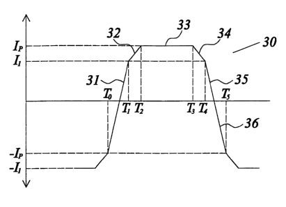
Referring to Fig. 4, at time TO there is instantaneous rise in current to a
preset
control value stored in the micro-controller 23. When this control value is
reached
2 0 the micro-controller 23 starts incrementing the DAC 25 according to a
program
stored on the micro-controller 23. The slew rate is therefore controlled and
ramps
the current in a controlled fashion. When the current reaches peak value the
micro-controller 23 stops incrementing the DAC 25 and holds it so that a
constant
current is obtained between time T2 and T3. At time T3 the micro-controller 23
2 5 decrements the DAC 25 so that the current level falls at the controlled
slew rate
until time T4 when the control value is reached.
Referring again to Fig. 4, there is illustrated the waveform of the current
used to
drive the gas discharge lamp 15. The shape of the waveform is slightly
exaggerated for ease of understanding. In practice the vertical portion would
not
be as inclined as shown as it occurs over a very short period of time. The
spacing
between TO and T1 and between T4 and T5 is thus much too great. Also the
discussion is directed largely to the positive current waveform above the line
identified generally by the reference numeral 30. This waveform and its shape
is
CA 02371527 2001-11-19
WO 00/70920 PCT/IE00/00067
controlled by the microcontroller 23. Between time TO and -T1 there is a
substantially instantaneous transition taking of the order of 10 ~,secs
between the
currents -11 and +11 and this forms an instantaneous transition phase with the
waveform 30 having a substantially vertical rising portion 31. From T1 to T2
the
current rises gradually in a transition phase providing an upwardly inclined
slew
rate portion 32 to a constant peak current IP. This steady peak portion of the
waveform is identified by the reference numeral 33. The current rise is at a
controlled current slew rate. The peak current is maintained between T2 and T3
when it starts to decay in another gradual transition phase providing a
declining
slew rate portion 34 until time T4 when the current is +11. Then between T4
and T5
another substantially instantaneous transition phase takes place between +11
and
-11 providing the waveform 30 with a substantially vertical falling portion 35
leading
into a mirror image negative waveform identified generally by the reference
numeral 36.
The abrupt sharp transition between -11 and +11 and obviously between +11 and
-11 minimises the time for which the arc is extinguished. This thus increases
considerably the probability that the new arc will form under identical or
very similar
conditions to that which pertained on forming the original arc. This
contributes to
the stability of the lamp. From the abrupt transition the controlled rise over
time to
peak current and then the controlled decay over time provides a suitable slew
rate
which obviates the possibility of acoustic harmonics being introduced which
will
cause the lamp mechanical assembly to "ring". It is believed that this ringing
can
cause fatigue of the welds and cause premature failure of the lamp. The gentle
slew rate reduces the amplitude of the acoustic harmonics. Finally, by
providing a
flat top waveform crest factor (the ratio of the peak value to the RMS value)
is
minimised.
Referring again to Fig. 2, there are four operational amplifiers 24(a), (b),
(c), (d)
3 0 with 24(a) measuring the current across the contacts 4 that is feeding
into the pulse
width modulator 22. The second operational amplifier 24(b) is giving an
indication
of that voltage by a filtered version of it to the microcontroller 23. The
next
operational amplifier 24(c) operates with a resistor 13 in such a way that it
feeds
back the voltage across the contacts 4 to the operational amplifier 24(c) that
feeds
CA 02371527 2001-11-19
WO 00/70920 PCT/IE00/00067
g _
into the microcontroller 23. The last operational amplifier 24(d) operates
with a
digital to analog converter (DAC) 25. The microcontroller 23 indicates to the
DAC
25 that it wants a particular power out, the DAC 25 generates the voltage,
sent
through the operational amplifier 24(d) and then to the pulse width modulator
22 so
that it controls the process to get the correct power to the contacts 4 and
hence the
gas discharge lamp 15.
As the gas discharge lamp 15 operates, due to wear and tear over time the
voltage
across the contacts 4 rises. In a typical gas discharge tube or lamp, it may
start at
80 volts and keep rising until it reaches 130 volts or even higher when
cycling
occurs. The lamp switches on and switches off over time which can vary from
milliseconds to minutes. In the present circuit this is prevented because the
circuit
can actually measure the voltage rise. Eventually there arrives a stage when
the
circuit could no longer drive the lamp, but the microcontroller 23 can switch
it off
before it gets to that stage. However, the voltage monitoring circuit can also
indicate that the voltage has risen above a predetermined level such as to
indicate
that the lamp has got close to the end of its useful life.
For a lamp to operate correctly, it is necessary that the ignition of the lamp
be
controlled in a suitable manner. In order for the lamps to be ignited they
need a
high voltage spike of several kilovolts. The present circuit provides a
voltage spike
of the order of 5 kilovolts for a brief period. This is achieved by using
ignition
MOSFETs 9(a) and 9(b). When, for example, the MOSFET 9(b) switches off the
voltage fed to inductor 6 to provide an output pulse rises so that at one of
the
contacts 4 a voltage spike of the order of 5 kilovolts is obtained. Once the
lamp
ignites then the inductor 6 controls the current going to the lamp so that it
acts as a
current limiter. Therefore the one inductor 6 carries out two tasks in the
circuit.
Another feature of the present invention is that a low frequency current
waveform
3 0 delivered to the lamp is provided by the ballast 1 which uses high
frequency
circuitry. This is achieved by commutating the MOSFETs 7(c) and 7(d) to change
the polarity of the waveform. The ballast 1 has the ability of monitoring the
lamp
voltage by regulating the power factor control voltage. Power to the lamp is
kept
constant by varying the pulse width from the pulse width modulator. This is
CA 02371527 2001-11-19
WO 00/70920 PCT/IE00/00067
- 9 -
achieved by varying the duty cycle via the MOSFET 11 to ensure constant power
to
the lamp. MOSFETs 7(a) and 7(b) can be used to compensate for any drop in
lamp current which can vary the width of the duty cycle. This method has the
further advantage that control of the lamp is independent of the mains.
On a fault occurring the microcontroller 23 can cause a signal to be delivered
to the
contacts 27 which contacts 27 can be then be used to either direct a signal to
a
central host station to indicate the fault or to cause a visible signaling
device to be
operated such as described in our co-pending PCT Patent Application
PCT/IE99/00044 filed the same day as Irish application No. 99 0396 on which
this
application is based and the disclosure of which is incorporated herein by
reference.
The use of the microcontroller 23 allows the waveform of the current to be
formed
in the desired shape and it will be appreciated that if other waveforms or
variations
on this waveform are found to be necessary for a particular construction of
gas
discharge tube that it can be relatively easily supplied.
Fig. 5 illustrates a waveform indicated generally by the reference numeral 40
in
2 0 which those parts of the waveform 40 identical to those of the waveform 30
are
identified by the same reference numerals. In this embodiment, the gradual
transition phase forms two substantially interconnected waveform portions 41
and
42 of varying rate of rise to and decline from the peak.
Referring now to Fig. 6 there is illustrated a still further waveform
indicated generally
by the reference numeral 50 in which parts similar to of the waveform 30 are
identified by the same reference numerals. In this embodiment the gradual
transition
phase forms an arcuate waveform portion 51 of substantially part sinusoidal
shape.
3 0 Fig. 7 illustrates another waveform indicated generally by the reference
numeral 60
and again in which parts similar to those described with reference to the
previous
drawings are identified by the same reference numerals. This waveform again
has a
gradual transition phase which forms an arcuate waveform portion 61.
CA 02371527 2001-11-19
WO 00/70920 PCT/IE00/00067
- 10 -
The pulse width modulator and the DAC could be incorporated into a digital
and/or
software implementation of their function.
While the above embodiment shows a particularly suitable way of providing the
necessary driver waveform, it will be appreciated by those skilled in the art
that
many other ways could be used to provide the waveform. The essence of the
invention is in the modification or alteration of the conventional waveform in
the
manner shown and not in the manner in which it is achieved. The present
arrangement is particularly advantageous in that it is a simple cost effective
and
efficient way of doing it. However, what must be appreciated is that a major
aspect
of the present invention is the recognition of the need to control the
waveform
accurately to provide better than existing lamp operating conditions. The
important
feature of the present invention is that it achieves both a quick zero cross
transition
to minimise the time for which the arc is extinguished while at -the same time
compensating for the introduction of acoustic harmonics. It is also accepted
that
experimentation may find that different shapes of waveform may be provided and
that the percentage rise in current instantaneously can vary depending on
particular operating conditions and in for particular constructions of gas
discharge
tube or lamp. Thus, it is envisaged that the instantaneous rise in current can
be
2 0 between 25% and 90% of the peak current. We have found that somewhere
between 70% and 80% is ideal but this may be due more to the particular gas
discharge tubes that have been used in tests to date than for any other
reason.
Similarly, it has been found that the controlled rise and decay takes place
over
between 20% and 60% of the cycle time. That is to say, for example, the rise
takes
place over between 10% and 30% of the cycle time, however, it is suggested
that
this may be more likely to be somewhat of the order of 15 to 25% but again
sufficient work has not been done to date to accurately assess what are either
the
correct levels of current that should be achieved instantaneously nor indeed
the
length of time under which the rise and decay between peak and that level of
current, that is to say the instantaneous current achieved should be arranged.
In the specification the terms "comprise, comprises, comprised and comprising"
or
any variation thereof and the terms "include, includes, included and
including" or any
CA 02371527 2001-11-19
WO 00/70920 PCT/IE00/00067
- 11 -
variation thereof are considered to be totally interchangeable and they should
all be
afforded the widest possible interpretation and vice versa.
The invention is not limited to the embodiment hereinbefore described, but may
be
varied in both construction and detail within the scope of the claims.