Note: Descriptions are shown in the official language in which they were submitted.
CA 02371531 2010-12-29
-1 -
IMAGE PROCESSOR FOR CAMERA MODULE
FIELD OF THE INVENTION
The invention relates to a compact printer system able to print full-color,
business card size documents from a
device about the size of a pen. The system includes various hot-connectable
modules that provide a range of functions. In
particular the invention relates to an image processor for a camera module.
BACKGROUND OF THE INVENTION
Microelectronic manufacturing techniques have led to the miniaturization of
numerous devices. Mobile phones,
personal digital assistant devices, and digital cameras are very common
examples of the miniaturization trend.
One device that has not seen the advantage of microelectronic manufacturing
techniques is the printer.
Commercially available printers are large compared to many of the devices they
could support For instance, it is impractical
to carry a color printer for the purpose of instantly printing photographs
taken with known compact digital cameras.
In order to construct a camera module for a compact printer system it is
necessary to address the problem of control
- of the image capture and transformation process. Methods of very large scale
integration and microelectronic manufacturing
are known but have not been applied to the needs of a compact printer system.
No suitable image processor exists for a
camera module that connects directly to a printer module.
SUMMARY OF THE INVENTION
Accordingly, in one aspect of the present invention there is provided a method
of image processing an image
in a camera module having an image sensor recording an image, said method
comprising the steps of:
capturing an image from said image sensor in a red, green, blue (RGB) form;
linearizing with reference to a look-up table the captured image to obtain a
linear RGB image;
planarizing the linear RGB image to obtain a planar linear RGB image;
storing the planar linear RGB image;
transforming said planar linear RGB image from a planar linear RGB form to a
L*a*b* form, the step of
transforming comprising the successive steps of:
rotating the image,
performing white balance and range expansion on the rotated image,
resampling the white balanced and range expanded rotated image, and
converting the resampled image from the RGB colour space to the L*a*b* colour
space, and
sharpening the converted image; and
transmitting said L*a*b* form image on a bus of a compact printer system.
According to another aspect of the present invention there is provided an
image processor for a camera module
having an image sensor that captures an image, said image processor
comprising:
a central processing unit;
program memory associated with said central processing unit, said program
memory storing program steps for
execution by said central processing unit to operate said camera module to
capture said image;
one or more interface units communicating with components of said camera
module;
image storage memory for storing said image;
an image capture unit in communication with said image storage memory, said
central processing unit and said
image sensor, said image capture unit capturing said image from said image
sensor and storing said image in said image
storage memory in planarized linear RGB form; and
CA 02371531 2010-12-29
- 2 -
an image enhancing unit in communication with said image storage memory to
transform said image from
planarized linear RGB form to L*a*b* form for transmission by a serial bus
interface, wherein said image enhancing unit
comprises:
a rotating unit for rotating the image,
a white balancing and range expansion unit connected to the rotating unit for
performing white balance
and range expansion on the rotated image,
a resampling unit connected to the white balancing and range expansion unit
for resampling the white
balanced and range expanded rotated image,
a colour conversion unit for converting the resampled image from the RGB
colour space to the L*a*b*
colour space, and
a sharpening unit for sharpening the converted image.
Further features of the invention will be evident from the following
description.
BRIEF DESCRIPTION OF THE DRAWINGS
In order to assist with describing preferred embodiments of the invention,
reference will be made to the following
figures in which:
FIG 1 is a printer module;
FIG 2 is a camera module;
FIG 3 is a memory module;
FIG 4 is a communication module;
FIG 5 is a flash module;
FIG 6 is a timer module;
FIG 7 is a laser module;
FIG 8 is an effects module;
FIG 9 is a characters module;
FIG 10 is an adaptor module;
FIG 11 is a pen module;
FIG 12 is a dispenser module;
FIG 13 is a first compact printer configuration;
FIG 14 is a second compact printer configuration;
FIG 15 is a third compact printer configuration;
FIG 16 is a fourth compact printer configuration;
FIG 17 is a block diagram of a controller for the camera module of FIG 2;
FIG 18 is a block diagram of the image capture unit;
CA 02371531 2001-11-23
WO 00/72265
PCT/AU00/00507
- 3 -
FIG 19 is a block diagram of the image enhancement unit;
FIG 20 is a block diagram of the white balance and range expansion process;
FIG 21 is a block diagram of the resample process;
FIG 22 is a block diagram of the color conversion process;
FIG 23 is a block diagram of the sharpen process;
DETAILED DESCRIPTION OF THE PREFERRED EMBODIMENTS
Referring to FIGs 1 to 12, there are shown various modules that together form
a compact printer system.
Individual modules can be attached and detached from the compact printer
configuration to allow a user-definable solution
to business-card sized printing. Images can also be transferred from one
compact printer to another without the use of a
secondary computer system. Modules have a minimal user-interface to allow
straightforward interaction.
A compact printer system configuration consists of a number of compact printer
modules connected together.
Each compact printer module has a function that contributes to the overall
functionality of the particular compact printer
configuration. Each compact printer module is typically shaped like part of a
pen, physically connecting with other
compact printer modules to form the complete pen-shaped device. The length of
the compact printer device depends on
the number and type of compact printer modules connected. The functionality of
a compact printer configuration depends
on the compact printer modules in the given configuration.
The compact printer modules connect both physically and logically. The
physical connection allows modules to
be connected in any order, and the logical connection is taken care of by the
compact printer Serial Bus - a bus that
provides power, allows the modules to self configure and provides for the
transfer of data.
In terms of physical connection, most compact printer modules consist of a
central body, a male connector at
one end, and a female connector at the other. Since most modules have both a
male and female connector, the modules can
typically be connected in any order. Certain modules only have a male or a
female connector, but this is determined by the
function of the module. Adaptor modules allow these single-connector modules
to be connected at either end of a given
compact printer configuration.
A four wire physical connection between all the compact printer modules
provides the logical connection
between them in the form of the compact printer Serial Bus. The compact
printer Serial Bus provides power to each
module, and provides the means by which data is transferred between modules.
Importantly, the compact printer Serial
Bus and accompanying protocol provides the means by which the compact printer
system auto-configures, reducing the
user-interface burden on the end-user.
Compact printer modules can be grouped into three types:
= image processing modules including a Printer Module (FIG 1), a Camera
Module (FIG 2),
and a Memory Module (FIG 3). Image processing modules are primarily what sets
the compact printer system apart from
other pen-like devices. Image processing modules capture, print, store or
manipulate photographic images;
= housekeeping modules including an Adapter Module (FIG 10), an Effects
Module (FIG 8), a
Communications Module (FIG 4), and a Timer Module (FIG 6). Housekeeping
modules provide services to other modules
or extended functionality to other modules; and
40= isolated modules including a Pen Module (FIG 11) and
a Laser Module (FIG 7). Isolated
modules are those that attach to the compact printer system but are completely
independent of any other module. They do
not necessarily require power, and may even provide their own power. Isolated
Modules are defined because the
functionality they provide is typically incorporated into other pen-like
devices.
SUBSTITUTE SHEET (RULE 26)
CA 02371531 2007-10-17
- 4
Although housekeeping modules and isolated modules are useful components in a
compact printer system, they
are extras in a system dedicated to image processing and photographic
manipulation. Life size (1:1) illustrations of the
compact printer modules are shown in FIGs 1 to 12, and example configurations
produced by connecting various modules
together are shown in FIGs 13 to 16.
FIG 1 shows a printer module that incorporates a compact printhead described
in co-pending United States
Patent Applications listed in the Background section of this application and
referred to herewith as a Memjet printhead.
The Memjet printhead is a drop-on-demand 1600 dpi inkjet printer that produces
bi-level dots in up to 4 colors to produce
a printed page of a particular width. Since the printhead prints dots at 1600
dpi, each dot is approximately 22.5 m in
diameter, and spaced 15.875pm apart. Because the printing is bi-level, the
input image should be dithered or error-
diffused for best results. Typically a Memjet printhead for a particular
application is page-width. This enables the
printhead to be stationary and allows the paper to move past the printhead. A
Memjet printhead is composed of a number
of identical 1/2 inch Memjet segments.
The printer module 10 comprises a body 11 housing the Memjet printhead. Power
is supplied by a three volt
battery housed in battery compartment 12. The printhead is activated to
commence printing when a business card (or
similar sized printable media) is inserted into slot 13. Male connector 14 and
female connector 15 facilitate connection of
other modules to the printer module 10.
FIG 2 shows a camera module 20. The camera module provides a point-and-shoot
camera component to the
compact printer system as a means of capturing images. The camera module
comprises a body 21 having a female
connector 22. A lens 23 directs an image to an image sensor and specialized
image processing chip within the camera 24.
A conventional view finder 25 is provided as well as a lens cap 26. An image
is captured when the Take button 27 is
pushed. Captured images are transferred to the Printer Module 10 for
subsequent printing, manipulation, or storage. The
Camera Module also contains a self-timer mode similar to that found on regular
cameras.
FIG 3 shows a Memory Module 30 comprising a body 31, LCD 32, IN button 33, OUT
button 34 and SELECT
button 35. The Memory Module 30 is a standard module used for storing
photographic images captured by the Camera 20.
The memory module stores 48 images, each of which can be accessed either at
full resolution or at thumbnail resolution.
Full resolution provides read and write access to individual images, and
thumbnail resolution provides read access to 16
images at once in thumbnail form.
The Memory Module 30 attaches to other modules via a female connector 36 or
male connector 37. The male
and female connectors allow the module to be connected at either end of a
configuration. Power is provided from the
Printer Module 10 via the Serial Bus.
A Communications Module 40 is shown in FIG 4. The communications module 40
consists of a connector 41
and a cable 42 that terminates in an appropriate connector for a computer
port, such as a USB port, RS232 serial port or
parallel port. The Communications Module 40 allows the compact printer system
to be connected to a computer. When so
connected, images can be transferred between the computer and the various
modules of the compact printer system. The
communications module allows captured images to be downloaded to the computer,
and new images for printing to be
uploaded into the printer module 10.
A Flash Module 50 is shown in FIG 5. The Flash Module 50 is used to generate a
flash with flash cell 51 when
taking photographs with the Camera Module 20. The Flash Module attaches to
other modules via female connector 52 and
male connector 53. It contains its own power source. The Flash Module is
automatically selected by the Camera Module
when required. A simple switch allows the Flash Module to be explicitly turned
off to maximize battery life.
FIG 6 shows a Timer Module 60 that is used to automate the taking of multiple
photos with the Camera Module
20, each photo separated by a specific time interval. The captured photos are
stored in Memory Module 30. Any flash
requirements are handled by the Camera Module 20, and can therefore be ignored
by the Timer Module. The Timer
Module 60 consists of a body 61 housing a LCD 62, START/STOP button 63 and
UNITS button 64. A SELECT button
CA 02371531 2001-11-23
WO 00/72265
PCT/AU00/00507
-5-
65 allows the user to select time units and the number of units are set by
UNITS button 64. The Timer Module 60 includes
a male connector 66 and female connector 67. The Timer Module takes its power
from the Printer Module 10 via the
Serial Bus.
A Laser Module 70 is shown in FIG 7. The Laser Module 70 consists of a body 71
containing a conventional
laser pointer operated by button 72. As the Laser Module is a terminal module
it only has one connector, which in the
example is a male connector 73. The Laser Module is an isolated module, in
that it does not perform any image capture,
storage, or processing. It exists as a functional addition to the compact
printer system. It is provided because laser pointer
services are typically incorporated into other pen-like devices. The Laser
Module contains its own power supply and does
not appear as a device on the Serial Bus.
The Effects Module shown in FIG 8 is an image processing module. It allows a
user to select a number of
effects and applies them to the current image stored in the Printer Module 10.
The effects include borders, clip-art,
captions, warps, color changes, and painting styles. The Effects Module
comprises a body 81 housing custom electronics
and a LCD 82. A CHOOSE button 83 allows a user to choose between a number of
different types of effects. A SELECT
button 84 allows the user to select one effect from the number of effects of
the chosen type. Pressing the APPLY button
85 applies the effect to image stored in the Printer Module 10. The Effects
Module obtains power from the Serial Bus.
Male connector 86 and female connector 87 allow the Effects Module to be
connected to other compact printer system
modules.
FIG 9 shows a Character Module 90 that is a special type of Effects Module
(described above) that only
contains character clip-art effects of a given topic or genre. Examples
include The Simpsons , Star Wars , Batman , and
Dilbert as well as company specific modules for McDonalds etc. As such it is
an image processing module. It consists
of a body 91 housing custom electronics and a LCD 92. SELECT button 93 allows
the user to choose the effect that is to
be applied with APPLY button 94. The Character Module obtains power from the
Serial Bus through male connector 95
and female connector 96.
The Adaptor Module 100, shown in FIG 10, is a female/female connector that
allows connection between two
modules that terminate in male connectors. A male/male connector (not shown)
allows connection between two modules
that terminate in female connectors. The Adaptor Module is a housekeeping
module, in that it facilitates the use of other
modules, and does not perform any specific processing of its own.
All "through" modules have a male connector at one end, and a female connector
at the other end. The modules
can therefore be chained together, with each module connected at either end of
the chain. However some modules, such as
the Laser Module 70, are terminating modules, and therefore have either a male
or female connector only. Such single-
connector modules can only be connected at one end of the chain. If two such
modules are to be connected at the one time,
an Adaptor Module 100 is required.
FIG 11 shows a Pen Module 110 which is a pen in a module form. It is an
isolated module in that it attaches to
the compact printer system but is completely independent of any other module.
It does not consume or require any power.
The Pen Module is defined because it is a convenient extension of a pen
shaped, pen sized device. It may also come with a
cap 111. The cap may be used to keep terminating connectors clean in the case
where the chain ends with a connector
rather than a terminating module.
To assist with accurately feeding a business card sized print media into slot
13 of the printer module 10, a
dispenser module 120 is provided as shown in FIG12. The dispenser module 120
comprises a body 121 that holds a store
of business card sized print media. A Printer Module 10 locates into socket
122 on the dispenser module 120. When
correctly aligned, a card dispensed from the dispenser module by slider 123
enters slot 13 and is printed.
In the sense that a minimum configuration compact printer system must be able
to print out photos, a minimum
compact printer configuration contains at least a Printer Module 10. The
Printer Module holds a single photographic
SUBSTITUTE SHEET (RULE 26)
CA 02371531 2001-11-23
WO 00/72265
PCT/AU00/00507
- 6 -
image that can be printed out via its Memjet printer. It also contains the 3V
battery required to power the compact printer
system.
In this minimum configuration, the user is only able to print out photos. Each
time a user inserts a business card
130 into the slot in the Printer Module, the image in the Printer Module is
printed onto the card. The same image is printed
each time a business card is inserted into the printer. In this minimum
configuration there is no way for a user to change
the image that is printed. The dispenser module 120 can be used to feed cards
130 into the Printer Module with a
minimum of fuss, as shown in FIG 13.
By connecting a Camera Module 20 to the minimum configuration compact printer
system the user now has an
instant printing digital camera in a pen, as shown in FIG 14. The Camera
Module 20 provides the mechanism for
capturing images and the Printer Module 10 provides the mechanism for printing
them out. The battery in the Printer
Module provides power for both the camera and the printer.
When the user presses the "Take" button 27 on the Camera Module 20. the image
is captured by the camera 24
and transferred to the Printer Module 10. Each time a business card is
inserted into the printer the captured image is
printed out. If the user presses "Take" on the Camera Module again, the old
image in the Printer Module is replaced by the
new image.
If the Camera Module is subsequently detached from the compact printer system,
the captured image remains in
the Printer Module, and can be printed out as many times as desired. The
Camera Module is simply there to capture
images to be placed in the Printer Module.
FIG 15 shows a further configuration in which a Memory Module 30 is connected
to the configuration of FIG
14. In the embodiment of FIG 15, the user has the ability to transfer images
between the Printer Module 10 and a storage
area contained in the Memory Module 30. The user selects the image number on
the Memory Module, and then either
sends that image to the Printer Module (replacing whatever image was already
stored there), or brings the current image
from the Printer Module to the specified image number in the Memory Module.
The Memory Module also provides a way
of sending sets of thumbnail images to the Printer Module.
Multiple Memory Modules can be included in a given system, extending the
number of images that can be
stored. A given Memory Module can be disconnected from one compact printer
system and connected to another for
subsequent image printing.
With the Camera Module 20 attached to a Memory Module/Printer Module compact
printer system, as shown in
FIG 15, the user can "Take" an image with the Camera Module, then transfer it
to the specified image number in the
Memory Module. The captured images can then be printed out in any order.
By connecting a Communications Module 40 to the minimum configuration compact
printer system, the user
gains the ability to transfer images between a PC and the compact printer
system. FIG 16 shows the configuration of FIG
15 with the addition of a Communications Module 40. The Communications Module
makes the Printer Module 10 and
any Memory Modules 30 visible to an external computer system. This allows the
download or uploading of images. The
communications module also allows computer control of any connected compact
printer modules, such as the Camera
Module 20.
In the general case, the Printer Module holds the "current" image, and the
other modules function with respect to
this central repository of the current image. The Printer Module is therefore
the central location for image interchange in
the compact printer system, and the Printer Module provides a service to other
modules as specified by user interaction.
A given module may act as an image source. It therefore has the ability to
transfer an image to the Printer
Module. A different module may act as an image store. It therefore has the
ability to read the image from the Printer
Module. Some modules act as both image store and image source. These modules
can both read images from and write
images to the Printer Module's current image.
The standard image type has a single conceptual definition. The image
definition is derived from the physical
SUBSTITUTE SHEET (RULE 26)
CA 02371531 2001-11-23
WO 00/72265
PCT/AU00/00507
- 7 -
attributes of the printhead used in the Printer Module. The printhead is 2
inches wide and prints at 1600dpi in cyan,
magenta and yellow bi-level dots. Consequently a printed image from the
compact printer system is 3200 bi-level dots
wide.
The compact printer system prints on business card sized pages (85mm x 55mm).
Since the printhead is 2 inches
wide, the business cards are printed such that 1 line of dots is 2 inches. 2
inches is 50.8mm, leaving a 2mm edge on a
standard business-card sized page. The length of the image is derived from the
same card size with a 2mm edge.
Consequently the printed image length is 81mm, which equals 5100 1600dpi dots.
The printed area of a page is therefore
81mm x 51mm, or 5100 x 3200 dots.
To obtain an integral contone to bi-level ratio a contone resolution of 267
ppi (pixels per inch) is chosen. This
yields a contone CMY page size of 850 x 534, and a contone to bi-level ratio
of 1:6 in each dimension. This ratio of 1:6
provides no perceived loss of quality since the output image is bi-level.
The printhead prints dots in cyan, magenta, and yellow ink. The final output
to the printed page must therefore
be in the gamut of the printhead and take the attributes of the inks into
account. It would at first seem reasonable to use the
CMY color space to represent images. However, the printer's CMY color space
does not have a linear response. This is
definitely true of pigmented inks, and partially true for dye-based inks. The
individual color profile of a particular device
(input and output) can vary considerably. Image capture devices (such as
digital cameras) typically work in RGB (red
green blue) color space, and each sensor will have its own color response
characteristics.
Consequently, to allow for accurate conversion, as well as to allow for future
image sensors, inks, and printers,
the CIE L*a*b* color model [CIE, 1986, CIE 15.2 Colorimetry: Technical Report
(2"d Edition), Commission
Internationale De l'Eclairage] is used for the compact printer system. L*a*b*
is well defined, perceptually linear, and is a
superset of other traditional color spaces (such as CMY, RGB, and HSV).
The Printer Module must therefore be capable of converting L*a*b* images to
the particular peculiarities of its
CMY color space. However, since the compact printer system allows for
connectivity to PCs, it is quite reasonable to also
allow highly accurate color matching between screen and printer to be
performed on the PC. However the printer driver or
PC program must output L*a*b*.
Each pixel of a compact printer image is therefore represented by 24 bits: 8
bits each of L*, a*, and b*. The total
image size is therefore 1,361,700 bytes (850 x 534 x 3).
Each image processing module is able to access the image stored in the Printer
Module. The access is either to
read the image from the Printer Module, or to write a new image to the Printer
Module.
The communications protocol for image access to the Printer Module provides a
choice of internal image
organization. Images can be accessed either as 850 x 534 or as 534 x 850. They
can also be accessed in interleaved or
planar format. When accessed as interleaved, each pixel in the image is read
or written as 24 bits: 8 bits each of L*, a*, b*.
When accessed as planar, each of the color planes can be read or written
independently. The entire image of L* pixels, a*
pixels or b* pixels can be read or written at a time.
As mentioned above, a camera, such as the camera module 20, acquires an image
in RGB format but the printer
module 10 prints the image in CMY format. The camera module includes an
application specific integrated circuit
configured as an image processor to collect an image from a CMOS image sensor
and transforms the image to a format
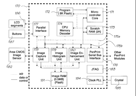
suitable for transmission to the image processor of the print module. FIG 17
shows a schematic of the image processor
170. Each element of the controller is described in detail below together with
examples of operation of the elements.
The image processor 170 is designed to be fabricated using a 0.25 micron CMOS
process, with approximately 4
million transistors, almost half of which are flash memory or static RAM. This
leads to an estimated area of 8mm2. The
image processor contains:
= a CPU/microcontroller core;
= program storage memory, which is suitably 8 Kbytes of flash memory;
SUBSTITUTE SHEET (RULE 26)
CA 02371531 2001-11-23
WO 00/72265
PCT/AU00/00507
- 8 -
= program variable storage, which is suitably 2 KByte of RAM;
= image processing units, including an image capture unit, image histogram
unit and an image enhancement unit;
= a Serial Bus Interface;
= a parallel interface;
The image processor may also include a number of housekeeping and
administration elements including;
= image storage RAM , which is suitably multi-level Flash memory;
= a memory decoder;
= a clock; and
= a joint test action group (JTAG) interface.
The image processor is intended to run at a clock speed of approximately 24
MHz on 3V externally and 1.5V
internally to minimize power consumption. The actual operating frequency will
be an integer multiple of the Serial Bus
operating frequency. The CPU is intended to be a simple micro-controller style
CPU, running at about 1 MHz, and can be
a vendor supplied core.
The image processor incorporates a simple micro-controller CPU core 171 to
synchronize image capture and
printing image processing chains and to perform general operating system
duties. A wide variety of CPU cores are
suitable, it can be any processor core with sufficient processing power to
perform the required calculations and control
functions fast enough to meet consumer expectations.
Since all of the image processing is performed by dedicated hardware, the CPU
does not have to process pixels.
As a result, the CPU can be extremely simple. An example of a suitable core is
a Philips 8051 micro-controller running at
about 1 MHz.
Associated with the CPU Core 171 is a Program ROM 172 and a small Program
Scratch RAM 173. The CPU
171 communicates with the other units within the image processor via memory-
mapped I/0 supported by a Memory
Decoder 174. Particular address ranges map to particular units, and within
each range, to particular registers within that
particular unit. This includes the serial interface 176 and parallel interface
177 described below.
The CPU Memory Decoder 174 is a simple decoder for satisfying CPU data
accesses. The Decoder translates
data addresses into internal register accesses over the internal low speed bus
175, and therefore allows for memory
mapped I/0 of image processor registers. The bus 175 includes address lines
I75a and data or control lines 175b.
The small Program Flash ROM 172 is incorporated into the image processor to
store simple sequences for
controlling the operation of the image processor 170. The ROM size depends on
the CPU chosen, but should not be more
than 8 Kbytes.
Likewise, a small scratch RAM 173 is incorporated into the image processor
for, primarily, program variable
storage. Since the program code does not have to manipulate images, there is
no need for a large scratch area. The RAM
size depends on the CPU chosen (e.g. stack mechanisms, subroutine calling
conventions, register sizes etc.), but should
not be more than about 2Kbytes
The Serial Bus interface 176, is connected to the internal chip low-speed bus
175. The Serial Bus is controlled
by the CPU 171 and preferably follows the USB protocol, although other
protocols may be suitable. The maximum speed
on the bus is 12 MBits/sec, although the maximum effective data transfer rate
is 8MBits/sec due to protocol overhead and
transmission redundancy. The Serial Bus is used to transmit commands and
images between the various modules of the
compact printer system and is described in a co-pending application titled
Modular Compact Printer System.
Since the image processor 170 is responsible for transmitting an image to the
Printer Module 10, the
transmission timing considerations are required for image processing
parameters. The time taken to transmit a complete
image (850 x 534 L*a*b*) is 1.36 seconds (850 x 534 x 3 x 8/ 8,000,000).
SUBSTITUTE SHEET (RULE 26)
CA 02371531 2001-11-23
WO 00/72265
PCT/AU00/00507
- 9 -
The parallel interface 177 connects the image processor to individual static
electrical signals. such as LCD
segments 186 and buttons 187 (eg. self timer). The CPU 171 is able to control
each of these connections as memory-
mapped I/0 via the low-speed bus 175. The following table shows the
connections to the parallel interface.
Connections to Parallel Interface
Connection Direction Pins
"Take" button In
Timer on/off switch In 1
A standard JTAG (Joint Test Action Group) Interface 183 may be included in the
image processor for testing
purposes. Due to the complexity of the chip, a variety of testing techniques
are required, including BIST (Built In Self
Test) and functional block isolation. An overhead of 10% in chip area is
assumed for overall chip testing circuitry.
The image processor 170 may also include a clock phase-locked loop 184 that
provides timing signals to the
controller. The clock 184 draws a base signal from crystal oscillator 185.
Some CPU include a clock so the clock 184 and
crystal 185 may not be required.
An Image Storage Memory 181 is used to store a captured image obtained from
the image sensor 182 via the
image capture unit 178. It is suitably analog multi-level Flash RAM (4-bits
per cell) so that the image is retained after the
power has been shut off. The Image Storage Memory is referred to as ImageRAM
for convenience Although Flash
memory is not required, multilevel Flash memory requires fewer gates than RAM,
and the use of 16-level Flash (4-bit per
cell) is possible as the occasional bit error in the image is not fatal
(compared to program code).
The image is written to ImageRAM 181 by the Image Capture Unit 178, and read
by image processing units
which are suitably an Image Histogram Unit 179 and the Image Enhancement Unit
180. The Image Histogram Unit 179
and the Image Enhancement Unit 180 could be embodied in a single image
processing unit but the inventors find that it is
convenient conceptually to treat the processes performed by each unit
separately. The CPU 171 does not have direct
random access to this image memory.
The Image Capture Unit 178 accepts pixel data from the image sensor 182 via an
Image Sensor Interface 188,
linearizes the RGB data via a lookup table 189, and finally writes the
linearized ROB image to ImageRAM 181 in planar
format. The process is shown in FIG 18.
The total amount of memory required for the planarized linear ROB image is
500.000 bytes (approximately 0.5
MB) arranged as follows:
= R: 425 x 267 = 113,475 bytes
= B: 425 x 267 = 113,475 bytes
= G: 425 x 537 = 226,950 bytes
The Image Sensor Interface (ISI) 188 is a state machine that sends control
information to the external CMOS
Image Sensor 182, including frame sync pulses and pixel clock pulses in order
to read the image. The ISI may be a
sourced cell from the image sensor manufacturer. The ISI is controlled by an
Image Capture Unit State Machine 190.
Although a variety of image sensors are available, only the Bayer color filter
array (CFA) is considered here by
way of example. Persons skilled in the art will be able to readily extend the
invention to other image sensor formats.
The image captured by the CMOS sensor (via a taking lens) is assumed to have
been sufficiently filtered so as to
remove any aliasing artifacts. The sensor itself has an aspect ratio of
approximately 3:2, with a resolution of 850 x 534
samples. The most likely pixel arrangement is the Bayer color filter array
(CFA), with each 2 x 2 pixel block arranged in a
mosaic of one red pixel, one blue pixel, and two green pixels on a diagonal of
the pixel block.
SUBSTITUTE SHEET (RULE 26)
CA 02371531 2001-11-23
WO 00/72265 PCT/AU00/00507
- 10 -
Each contone sample of R, G. or B (corresponding to red, green, and blue
respectively) is 10-bits. Note that each
pixel of the mosaic contains information about only one of R, G, or B.
Estimates of the missing color information must be
made before the image can be printed.
The CFA is considered to perform some amount of fixed pattern noise (FPN)
suppression. Additional FPN
suppression may required.
The image sensor is unlikely to have a completely linear response. Therefore
the 10-bit RGB samples from the
CFA must be considered to be non-linear. These non-linear samples are
translated into 8-bit linear samples by means of a
lookup table (one table per color). The lookup table 189 is a ROM mapping the
sensor's RGB response to a linear RGB.
As such, the ROM is 3 KBytes (3 x 1024 x 8-bits). Ten bits of address come
from the ISI, and two bits of TableSelect are
generated by the Image Capture Unit's State Machine 190.
The Image Capture Unit's State Machine 190 generates control signals for the
Image Sensor Interface, and
generates addresses for linearizing the RGB and for planarizing the image
data.
The control signals sent to the ISI inform the ISI to start capturing pixels,
stop capturing pixels etc.
The 2-bit address sent to the Lookup Table matches the current line being read
from the ISI. For even lines (0, 2,
4 etc.), the 2-bit address is Red, Green, Red, Green etc. For odd lines (1, 3,
5 etc.), the 2-bit address is Green, Blue. Green,
Blue. This is true regardless of the orientation of the camera.
A 21-bit address is sent to the Image RAM as the write address for the image.
Three registers hold the current
address for each of the red, green, and blue planes. The addresses increment
as pixels are written to each plane.
The Image Capture Unit contains a number of registers which are summarized in
the following table.
Registers in Image Capture Unit
Name Bits Description
MaxPixels 10 Number of pixels each row
MaxRows 10 Number of rows of pixels in image
CurrentPixel 10 Pixel currently being fetched
CurrentRow 10 Row currently being processed
NextR 19 The address in Image RAM to store the next
Red pixel. Set to start
address of red plane before image capture. After image capture, this
register will point to the byte after the red plane.
NextG 19 The address in Image RAM to store the next
Green pixel. Set to start
address of green plane before image capture. After image capture,
this register will point to the byte after the green plane.
NextB 19 The address in Image RAM to store the next
Blue pixel. Set to start
address of blue plane before image capture. After image capture,
this register will point to the byte after the blue plane.
EvenEven 2 Address to use for even rows / even pixels
EvenOdd 2 Address to use for even rows / odd pixels
OddEven 2 Address to use for odd rows / even pixels
OddOdd 2 Address to use for odd rows / odd pixels
Go 1 Writing a 1 here starts the capture.
Writing a 0 here stops the image
capture. A 0 is written here automatically by the state machine after
MaxRows of MaxPixels have ben captured.
SUBSTITUTE SHEET (RULE 26)
CA 02371531 2001-11-23
WO 00/72265
PCT/AU00/00507
- 11 -
In addition, the Image Sensor Interface 188 will contain a number of
registers. The exact number of registers
will depend on the Image Sensor chosen.
The Image Histogram Unit (IHU) 179 is designed to generate histograms for
planar format images with samples
of eight bits each. The Image Histogram Unit is typically used three times per
print. Three different histograms are
gathered, one per color plane. Each time a histogram is gathered, the results
are analyzed in order to determine the low and
high thresholds, scaling factors etc. for use in the remainder of the print
process. Suitable histogram processes will be
known to persons skilled in the art.
The histogram itself is stored in a 256-entry RAM, each entry being 18 bits.
The histogram RAM is only
accessed from within the IHU. Individual entries are read from and written to
as 18-bit quantities.
The Image Enhancement Unit (IEU) 180 provides the interface between the Image
RAM 181 and the Serial Bus
Interface 176, as shown in FIG 19. The IEU takes a planarized linear RGB
obtained from a CFA format captured image
from the ImageRAM, and produces a fully populated L*a*b* image of resolution
850 x 534 for subsequent transmission
to the Printer Module 10 via the Serial Bus Interface 176.
The image enhancement process includes the following functions:
15Gather Statistics;
=
= Rotate Image;
= White Balance and Range Expansion;
= Resample;
= Convert to L*a*b*.
= Sharpen;
The IEU 180 performs all of these functions with the exception of Gather
Statistics. To perform the Gather
Statistics step, the CPU calls the Image Histogram Unit 179 three times (once
per color channel), and applies simple
thresholding algorithms.
In terms of speed, the IEU is producing data for the Serial Bus Interface.
Given that the Serial Bus Interface
transmits at an effective rate of 8 MHz, and the image processor 170 runs at
24 MHz, it takes the serial interface 72 cycles
to transmit the 24 bits for each pixel (3 colors @ 8 bits per color @ 3 cycles
to transfer each bit). The IEU therefore has 72
cycles to produce each L*a*b* triplet.
The IEU performs the four processes shown in FIG 19 in parallel. The first
process performs White Balance and
Range Expansion. The second process performs Resampling. The third performs
color conversion, and the fourth
performs sharpening. The output from the IEU is directly sent to the Serial
Bus Interface for transmission to the Printer
Module. The processes are connected via buffers, each typically only a few
bytes. The structure of the IEU is shown in
FIG 19. The buffer sizes are summarized in the following table.
Buffer sizes for Image Enhancement Unit
Buffer Size (bytes) Composition of Buffer
Buffer A 172.5 Red Buffer = 6 lines of 6 entries @ 10-bits
each = 45 bytes
Blue Buffer = 6 lines of 6 entries @ 10-bits each = 45 bytes
Green Buffer = 11 lines of 6 entries @ 10-bits each = 82.5 bytes
Buffer B 22.5 2 sets of 3 RGB pixels = 2 x 3 x 3 entries @ 10-
bits each = 180 bits
Buffer C 20 5 x 4 RAM
3 lines of 4 entries of L @ 8-bits each = 12 bytes
2 colors x 4 entries @ 8-bits each = 8 bytes
Buffer D 6 2 L*a*b* pixels = 2 x 3 entries @ 8-bits each = 6
bytes
SUBSTITUTE SHEET (RULE 26)
CA 02371531 2001-11-23
WO 00/72265
PCT/AU00/00507
- 12 -
The task of loading Buffer A 192 from the ImageRAM 181 involves the steps of
white balance and range
expansion 191. The pixels must be produced for Buffer A fast enough for their
use by the Resampling process. This means
that during a single group of 72 cycles, this unit must be able to read,
process, and store 6 red pixels, 6 blue pixels, and 11
green pixels.
Once a given pixel has been read from the appropriate plane in the image
store, it must be white balanced and its
value adjusted according to the range expansion calculation defined as:
Pixel' = (Pixel ¨ LowThreshold) x Ran geScaleFactor
where RangeScaleFactor=256/(HighThreshold ¨ LowThreshold)
The process simply involves a single subtraction (floor 0), and a multiply
(255 ceiling), both against color
specific constants. The structure of this unit is shown in FIG 20.
The red, green and blue low thresholds 199, together with the red, green, and
blue scale factors 200 are
determined by the CPU 171 after generating the histograms for each color plane
via the Image Histogram Unit.
Depending on whether the current pixel being processed in the pipeline is red,
green, or blue, the appropriate
low threshold and scale factor is multiplexed into the subtract unit and
multiply unit, with the output written to the
appropriate color plane in Buffer A.
The Subtract unit subtracts the 8-bit low Threshold value from the 8-bit Image
RAM pixel value, and has a floor
of O. The 8-bit result is passed on to the specialized 8 x 8 multiply unit,
which multiplies the 8-bit value by the 8-bit scale
factor (8 bits of fraction, integer=1). Only the top 10 bits of the result are
kept, and represent 8 bits of integer and 2 bits of
fraction. The multiplier has a result ceiling of 255, so if any bit higher
than bit 7 would have been set as a result of the
multiply, the entire 8-bit integer result is set to Is, and the fractional
part set to O.
Apart from the subtraction and multiply units, the majority of work in this
unit is performed by the Address
Generator 201, which is effectively the state machine for the unit. The
address generation is governed by two factors: on a
given cycle, only one access can be made to the Image RAM, and on a given
cycle, only one access can be made to Buffer
A. Of the 72 available cycles, 3 sets of 16 cycles are used by the Resampler
for reading Buffer A. The actual usage is 3
sets of 24 cycles, with 16 reads followed by 8 wait cycles. That gives a total
of 24 available cycles for 23 writes (6 red, 6
blue, 11 green). This means the two constraints are satisfied if the timing of
the writes to Buffer A coincide with the wait
cycles of the Resampler.
Buffer A holds the white-balanced and range-expanded pixels at the original
capture spatial resolution. Each
pixel is stored with 10 bits of color resolution, compared to the ImageRAM
image storage color resolution of 8 bits per
pixel.
Buffer A is arranged as three separately addressable buffers 192r, 192g, 192b -
one for each color plane of red,
green, and blue.
During the course of 72 cycles, 16 entries are read from each of the three
buffers three times by the Resampling
process. and up to 29 new values are written to the three buffers (the exact
number depends on the scale factor and the
current sub-pixel position during resampling). The buffers must be wide enough
so that the reading and writing can occur
without interfering with one another. During the read process, four pixels are
read from each of six rows. On average each
input pixel is used twice.
The green plane has a D value of 0.5 for resampling, indicating that four
sample positions can be contained
within two CFA pixel positions. However, each row of green samples only holds
every alternate pixel. This means that
only four samples are required per row (worst case is 4, not 3, due to a worst
case initial position). Movement in Y
indicates the requirement of an additional sample column, making five.
Finally, an additional sample column is required
for writing. This gives a total of six samples per row. Seven rows are
required for a single sample. To generate the three
sets of RGB pixels for each X position. the maximum movement in Y will be two
rows. Movement in X adds one sample
row above and below. Consequently a total of 11 rows are required.
SUBSTITUTE SHEET (RULE 26)
CA 02371531 2001-11-23
WO 00/72265 PCT/AU00/00507
- 13 -
The red and blue planes have a D value of 0.5 for resampling, indicating that
4 locations can be contained within
two samples. Four samples per row are required for the resampling process,
which is further increased to six samples to
match the green plane (for startup purposes). Six rows are required to cater
for movement in Y.
Each sub-buffer is implemented as a RAM with decoding to read or write a
single 10-bit sample per cycle. The
sub-buffers are summarized in the following table, and consume less than 175
bytes.
Sub-Buffer Summary
Buffer Composition Bits
Red Buffer 6 rows x 6 samples x 10-bits 360
Blue Buffer 6 rows x 6 samples x 10-bits 360
Green Buffer 11 rows x 6 samples x 10 bits 660
The Resample process is responsible for generating the full complement of R,
G, and B pixels for each CFA
coordinate by appropriate resampling of the white-balanced and range-expanded
R, G, and B planar images.
The time allowed for producing the components of R. G, and B is 72 cycles.
However we must effectively
produce RGB values for three pixel coordinates: the pixel in question, and the
pixel above and below. Thus we have 72
cycles in which to calculate three RGB samples.
Buffering RGB values to save recalculation requires too much memory, and in
any case, there is sufficient time
to generate the RGB values.
The resampling process can be seen as three sets of RGB generation, each of
which must be completed within
24 cycles (for a total maximum elapsed time of 72 cycles). The process of
generating a single RGB value can in turn be
seen as three processes performed in parallel: the calculation of R. the
calculation of G, and the calculation of B, all for a
given pixel coordinate. This is effectively running three image reconstruction
filters, one on each channel of the image. In
the case of the image processor 170 we perform image reconstruction with five
sample points, requiring four coefficients
in a convolution kernel (since one coefficient is always 0 and thus the sample
point is not required).
Consequently, calculation of the medium resolution R pixel is achieved by
running an image reconstruction
filter on the R data. Calculation of the medium resolution G pixel is achieved
by running an image reconstruction filter on
the G data, and calculation of the medium resolution B pixel is achieved by
running an image reconstruction filter on the
B data. Although the kernels are symmetric in x and y, they are not the same
for each color plane. R and B are likely to be
the same kernel due to their similar image characteristics, but the G plane,
due to the rotation required for image
reconstruction, must have a different kernel. A high level view of the process
can be seen in FIG 21.
The resampling process can only begin when there are enough pixels in Buffer A
for the current pixel line being
generated. This will be the case once four columns of data have been written
to each of the color planes in Buffer A. The
Resampling process must stall until that time.
To calculate a given color plane's medium resolution pixel value, we have 24
cycles available. To apply the
kernel to the 4 x 4 sample area, we apply a 1D kernel (indexed by x) on each
of the four rows of four input samples. We
then apply the ID kernel (indexed by y) on the resultant four pixel values.
The final result is the output resampled pixel.
Applying a single coefficient each cycle gives a total of 16 cycles to
generate the four intermediate values, and four cycles
to generate the final pixel value, for a total of 20 cycles.
With regards to precision, the input pixels are each 10 bits (8:2), and kernel
coefficients are 12 bits. We keep 14
bits of precision during the four steps of each application of the kernel
(8:6). but only save 10 bits for the result (8:2). Thus
the same convolve engine can be used when convolving in x and y. The final
output of R, G, or B is only 8 bits.
The process of resampling then, involves 20 cycles, as shown in the following
table. Note that Row I, Pixel 1
etc. refers to the input from Buffer A, and is taken care of by an Address
Generator.
SUBSTITUTE SHEET (RULE 26)
CA 02371531 2001-11-23
WO 00/72265
PCT/AU00/00507
- 14 -
The 20 Cycle Resample
Cycle Kernel Apply Kernel to: Store
Result in
1 X[1] Row 1, Pixel 1 TMP
2 X[2] Row 1, Pixel 2 TMP
3 X[3] Row 1, Pixel 3 TMP
4 X[4] Row 1, Pixel 4 TMP, VI
5 X[1] Row 2, Pixel I TMP
6 X[2] Row 2, Pixel 2 TMP
7 X[3] Row 2, Pixel 3 TMP
8 X[4] Row 2, Pixel 4 TMP, V2
9 X[1] Row 3, Pixel I TMP
10 X[2] Row 3, Pixel 2 TMP
11 X[3] Row 3, Pixel 3 TMP
12 X[4] Row 3, Pixel 4 TMP, V3
13 X[1] Row 4, Pixel I TMP
14 X[2] Row 4, Pixel 2 TMP
15 X[3] Row 4, Pixel 3 TMP
16 X[4] Row 4, Pixel 4 TMP, V4
17 Y[1] VI TMP
18 Y[2] V2 TMP
19 Y[3] V3 TMP
20 Y[4] V4 TMP (for output)
Buffer B 194 holds three complete sets of ROB pixel values (10-bits per color
component) for a given CFA
coordinate in a double buffered format (one set of 3 ROB pixels is being read
by the Color Convert process, while the
other is being written to 10-bits at a time by the Resample process).
The values are moved from the first ROB buffer to the second once the Color
Convert and Resample processes
have both finished. This can simply be achieved by a Select bit that is
toggled, rather than physically transferring the data
from one set of 9 bytes to the other.
The color conversion process 195 must produce contone L*a*b* pixels for the
Sharpen process within 72
cycles. Since the sharpening process only requires the L* values corresponding
to the first and third ROB sets, and only
requires the full L*a*b* set for the second ROB set, we have 72 cycles in
which to perform 5 color conversions (three sets
of ROB to L*, and I set each of ROB to a* and ROB to b*).
The process requires 14 cycles per color component, leading to a total of 70
cycles for five conversions (leaving
2 cycles spare).
The conversion is performed as tri-linear interpolation described in co-
pending application titled Color
Conversion Method for Compact Printer System. Three 17 x 17 x 17 x 8-bit
lookup tables 202 are used for the conversion
process: ROB to L*, ROB to a*, and ROB to b*.
Address generation for indexing into the lookup tables is straightforward. We
use the four most significant bits
of each 8-bit color component for address generation, and the four least
significant bits of each 8-bit color component for
interpolating between values retrieved from the conversion tables. The
addressing into the lookup table requires an adder
due to the fact that the lookup table has dimensions of 17 rather than 16.
Fortunately. multiplying a 4-bit number X by 17
is an 8-bit number XX, and therefore does not require an adder or multiplier,
and multiplying a 4-bit number by 172 (289)
is only slightly more complicated, requiring a single add.
Although the interpolation could be performed faster, a single adder is used
to generate addresses and have a
single cycle interpolation unit. Consequently it is possible to calculate the
interpolation for generating a single color
component from ROB in 14 cycles in interpolator 203. The process must be
repeated five times, once for each color
conversion. Faster methods are possible, but not necessary.
A block diagram of the color conversion process is shown in FIG 22. The basic
14 cycle color conversion
process is run five times as follows:
= on RGBI to generate L*1
SUBSTITUTE SHEET (RULE 26)
CA 02371531 2001-11-23
WO 00/72265
PCT/AU00/00507
- 15 -
= on RGB2 to generate L*2
= on RGB3 to generate L*3
= on RGB2 to generate a*
= on RGB2 to generate b*
Address generation for writing to Buffer C makes use of the cyclical nature of
Buffer C. The address consists of
a 2-bit column component (representing which of the four columns should be
written to), and a 3-bit value representing
L* I, L*2, L*3, a*, or b*. The column number starts at 0 each new line and
increments (with wrapping) every 72 cycles.
Buffer C 196 accepts the output from the Color Convert process 195, where a
complete L*a*b* pixel is
generated from the RGB equivalent for a given pixel coordinate. Buffer C is
used by the Sharpen process 197, which
requires a 3 x 3 set of luminance values centered on the pixel being
sharpened.
Consequently, during the sharpening process, there is need for access to the 3
x 3 array of luminance values, as
well as the corresponding a*b* value for the center luminance pixel. At the
same time, the next three L*a*b* values must
be calculated from the ROB values by the Color Convert process.
The actual implementation of Buffer C is simply as a 4 x 5 (20 entry) 8-bit
RAM, with the addressing on read
and write providing the effective shifting of values. A 2-bit column counter
can be incremented with wrapping to provide
a cyclical buffer, which effectively implements the equivalent of shifting the
entire buffer's data by I column position.
The fact that the fourth column of a*b* data is not required is not relevant,
and merely uses 2 bytes at the saving of not
having to implement complicated shift and read/write logic. In a given cycle,
the RAM can either be written to or read
from. The read and write processes have 72 cycles in which to complete in
order to keep up with the transmission process.
The Sharpen Unit 197 performs a sharpening process which involves a highpass
filter of the luminance channel
of the image (the L* channel). The highpass filter used is a basic highpass
filter using a 3 x 3 convolution kernel.
The high pass filter is calculated over ten cycles. The first cycle loads the
temporary register with eight times the
center pixel value (the center pixel shifted left by 3 bits). The next eight
cycles subtract the remaining eight pixel values,
with a floor of 0. Thus the entire procedure can be accomplished by an adder.
Cycle 10 involves the multiplication of the
result by a constant. This constant is the representation of 1/9, but is a
register to allow the amount to be altered by
software by some scale factor.
The resultant sharpened L* is written out to Buffer D 198 during cycle 11, and
the a*, and b* color components
are copied to Buffer D during cycles 12 and 13. The structure of the Sharpen
unit can be seen in FIG 23.
The adder unit 204 connected to Buffer C is a subtractor with a floor of 0.
TMP 205 is loaded with 8 x the first
L value during cycle 0 (of 75), and then the next 8 L values are subtracted
from it. The result is not signed, since the
subtraction has a floor of 0.
During the 10th cycle (Cycle 9), the 11 bit total in TMP is multiplied by a
scale factor 206 (typically 1/9, but
under software control so that the factor can be adjusted) and written back to
TMP. Only 8 integer bits of the result are
written to TMP (the fraction is truncated), so the limit from the multiply
unit is 255. If a scale factor of 1/9 is used, the
maximum value written will be 226 (255 x 8 / 9). The scale factor is 8 bits of
fraction, with the high bit representing 1/8.
Address Generation 207 is straightforward. Writing to Buffer D is simply L*,
a*, and b* in cycles 11, 12, and 13
respectively. Reading from Buffer C makes use of the cyclical nature of Buffer
C. The address consists of a 2-bit column
component (representing which of the four columns should be read), and a 3-bit
value representing L*1, L*2, L*3, a*, or
b*. The column number starts at 1 each line and increments (with wrapping)
every 72 cycles.
Sharpening can only begin when there have been sufficient L*a*b* pixels
written to Buffer C (so that the
highpass filter is valid). The sharpen process must therefore stall until the
color conversion process has written three
columns of data to Buffer C.
SUBSTITUTE SHEET (RULE 26)
CA 02371531 2001-11-23
WO 00/72265 PCT/AU00/00507
- 16 -
Buffer D 198 holds a complete L*a*b* pixel value (8-bits per color component)
ready to be transmitted by the
Serial Bus Interface 176 to the Printer Module 10. Buffer D is a double
buffered format (one L*a*b* pixel is being read
by the Serial Bus Interface process. while the other is being written to by
the Sharpen process during a 72 cycle period).
The values are moved from the first buffer to the second once the Serial Bus
Interface has transmitted all 24 bits
of L*a*b*. As with Buffer B, the double buffering can simply be achieved by a
Select bit that is toggled, rather than
physically transferring the data from one set of 3 bytes to the other. The
Serial Bus Interface supplies the WriteEnable
signal for the transfer.
It will be appreciated that the processes described herein are simple
operations on each value stored in an array
of values. Address generation satisfies the requirements of accessing array
locations in the appropriate order for reading
and writing.
Throughout the specification the aim has been to describe the preferred
embodiments of the invention without
limiting the invention to any one embodiment or specific collection of
features. Persons skilled in the relevant art may
realize variations from the specific embodiments that will nonetheless fall
within the scope of the invention.
SUBSTITUTE SHEET (RULE 26)