Note: Descriptions are shown in the official language in which they were submitted.
- CA 02371891 2001-08-16
I
SPECIFICATION
TIlVIITTG RECOVERY DEVICE AND DEMODULATOR USING THE
SAME
TECHNICAL FIELD
The present invention relates to a timing recovery device and a
demodulator and, more particularly, to a timing recovery device and a
demodulator suitable for use in a broadband digital radio communication
system in which a burst signal begins with a preamble.
BACKGROUND ART
For a timing recovery device of a demodulator for a conventional
broadband digital radio communication system which employs a preamble
signal, there are described two schemes, for example, in literature "Carrier-
Clock Simultaneous Recovery Scheme" by Nagura, Matsumoto, Kubota and
Kato, The Institute of Electronics, Information and Communication Engineers,
Technical Report of IEICE, RCS94-60, pp.7-12, September 1994.
The one scheme is to estimate a timing phase from a preamble signal
now widely used for OQPSK modulation. This preamble signal is a signal
(of a "1101" pattern, for instance) which effects an alternate transition
between two adjacent Nyquist points in a complex plane upon each
occurrence of a symbol. A patent for this scheme is "Burst Signal
Demodulation Circuit" (Pat. Appln. Laid-Open No. 35956/95, Inventors:
Matsumoto and Kato).
The other scheme is to estimate a timing phase from a preamble signal
widely used for QPSK modulation. This preamble signal is a "0~"
' CA 02371891 2001-08-16
2
modulation signal (of a "1001" pattern, for instance) which effects an
alternate transition between two origin-symmetric Nyquist points in a
complex plane upon each occurrence of a symbol. A patent for this scheme
is "Burst Signal Demodulation Circuit" (Pat. Appln. Laid-Open No. 46658/96,
Inventors: Nagura, Matsumoto and Kato).
According to these schemes, both of which utilize the fact that either
preamble signal has a frequency component 1/2 that of a symbol frequency
(fs), the receiver side calculates the correlation between the preamble signal
and a 1/2 symbol frequency component exp[ jn(fs)t] output from a VCO, and
estimates the timing phase from a vector angle indicated by the correlation
value.
In either scheme the data sampling rate is only 2 [sample/symbol];
since this sampling rate is 1/2 the minimum value of the sampling rate (=4
[sample/symbol] needed in a conventional scheme which estimates the timing
phase from the correlation between a nonlinearly processed signal (for
example, an envelope) and a symbol frequency component exp[ j2~(fs)t] as
described in, for example, literature "Signal Detecting System and Burst
Demodulating Equipment" (Pat. Appln. Laid-Open No. 141048/94, Inventor:
Yoshida), the reduction of the sampling rate permits reduction of the power
consumption of the receiver. The above-mentioned two schemes (Pat. Appln.
Laid-Open No. 235956/95 and Pat. Appln. Laid-Open No. 46658/96) will be
described below in detail.
A description will be given first of a timing recovery scheme (pat.
Appln. Laid-Open 235956/95) that uses the preamble ("1101" pattern) signal
which effects an alternate transition between two adjacent Nyquist points in a
complex plane upon each occurrence of a symbol.
Fig. 17 is a block diagram depicting the above-mentioned demodulator
CA 02371891 2001-08-16
3
containing a timing recovery device. In Fig. 17, reference numeral 100
denotes an antenna, 200 frequency converting means, 301 and 302 A/D
converters, 400 a timing recovery device, and 500 data decision means; and in
the timing recovery device 400, reference numeral 401 denotes one-symbol
delay means, 402 conjugate complex multiplying means, 403 timing phase
difference calculating means, and 404 a VCO.
Next, the operation of the conventional demodulator will be described.
The antenna 100 receives an RF band preamble signal, and the frequency
converting means 200 frequency-converts the RF band preamble signal to a
base band preamble signal.
Fig. 18 is a signal space diagram of the base band preamble signal
("1101" pattern. In Fig. 18, reference character 8c denotes the carrier phase
of the received signal; the preamble signal effects an alternate transition
between Nyquist points "A" and "B" in the figure upon each occurrence of a
symbol. The vector angle of the Nyquist point "A" is (6c-45) (deg), and the
vector angle of the Nyquist point "B" is (8c+45) [deg]; the difference between
the vector angles of the Nyquist points "A" and "B" is 90 [deg].
The A/D converter 301 samples an in-phase component of the base
band preamble signal at a time t=i+iT/2 (where I=1,2,3,..., i is a timing
error
(-T/2<_i<T/2) and T is a symbol period), and outputs a sampled preamble data
sequence Ip; (where i=1,2,3,...). Similarly, the A/D converter 302 samples a
quadrature component of the base band preamble signal at a time t=-c+iT/2,
and outputs a samples preamble data sequence Qp; (where I=1,2,3,...).
Therefore, it is apparent that the sampling rate is 2[sample/symbol].
The sampling is performed by the leading edge of a recovered sample clock
output from the timing recovery device 400 of the following stage, and during
a timing phase estimating operation no phase control of the recovered sample
CA 02371891 2001-08-16
4
clock is effected.
The timing recovery device 400 uses the preamble data sequence Ip;
(where i=1,2,3, ...) and the preamble data sequence Qp; (where i=1,2,3,...) to
calculate the timing error i, and exercises phase control of the recovered
sample clock and a recovered symbol clock to cancel the timing error i.
The recovered symbol clock mentioned herein is a clock of the symbol
period obtained by frequency dividing the recovered sample clock down to
1I2.
The data decision means 500 latches, by the recovered symbol clock,
data at the Nyquist points from significant random data sequences Id; and Qd;
(where i=1,2,3, . . . ) following the preamble after cancellation of the
timing
error i by the timing recovery device 400. And the data decision means uses
the latched Nyquist point data to decide data, and outputs demodulated data.
Next, the operation of the timing recovery device 400 will be
described. The one-symbol delay means 401 delays the preamble data
sequence Ip; (where i=1,2,3, . . . ) and the preamble data Qp; (where i=1,2,3,
. . . )
by a one-symbol time interval, and the conjugate complex multiplying means
402 performs conjugate complex multiplications of the preamble data
sequences (Ip;, Qp;) and one-symbol old preamble data sequences (Ip;_Z, Qp;_Z)
by the following equations.
Id(IPaXIpa-2)+(QpaXQP~-a) (la)
Qd~ (Qp~XIP~-2)+(Ip~xPQi_a) (1b)
By this processing, the preamble signal is differential-detected. With
such processing, it is possible to obtain a preamble signal which effects an
alternate transition between points "C" and "D" upon each occurrence of a
symbol independently of the carrier phase 6c as depicted in Fig. 19. The
phase 6x(t) indicated by this preamble signal has a 1/2 symbol frequency
CA 02371891 2001-08-16
- ' S
- component since it makes a phase transition from +90 [deg] to -90 [deg] and
a phase transition from -90 [deg] to +90 [deg] alternately with one symbol
period as depicted in Fig. 20.
Then, the timing phase difference calculating means 403 calculates the
correlation between the phase 6x(t) and the 1/2 symbol frequency component
exp[-jn(fs)t] output from the VCO. Concretely, letting the phases of the
signals (ID;, QD;) be represented by 8x;, the timing phase difference
calculating means performs the following multiplications
MI; 6X;xcos~i/2 (2a)
MQ; 6X;xsinni/2 (2b)
The timing phase difference calculating means averages the multiplied
results (NIT;, MQ;), and outputs a correlation value (EMI, EMQ).
Incidentally, since in the multiplications of Equations (2a) and (2b)
cos~i/2=1,0,-1,0,... and sinni/2=0,1,0,-1,..., the above-said correlation
values (EMI, EMQ) can easily be obtained. For example, in the case of
averaging the multiplied values over four symbols, the correlation value (EMI,
EMQ) can be obtained by the following equations.
EMI=(ex; ex;+4+ex;+4 ex;+6
+ex;+g ex;+,o+ex;+12 ex;+14)/s (3a)
EMQ=(8X;+i-6X;+3+6X;+s-6X;+76
+8X;+9 exa+u+6X;+~3 ex.+~s)/g (3b)
The vector angle that this correlation value indicates
QT tari ' (EMQ/EMI)
is a timing phase difference when normalized with two symbol periods (2T),
and hence the timing phase difference 8s [deg] when normalized with the
symbol period (T) is obtained by the following equation.
8s=26Tmod360 (4)
CA 02371891 2001-08-16
6
- The relationship between the timing phase difference 0s and the
timing error i is as follows:
In the case of 8s>180 [deg],
i=(6s-360)T/360 (5a)
In the case of 8<_180 [deg]
i=(6s)T/360 (5b)
For example, in the case where the phase signal 6X(t) is sampled at
the timing shown in Fig. 20 to obtain a data sequence {8X;, 6X;+1, 6X;+2,
8X;+3,
. . . } , such a correlation value (EMI, EMQ) and a timing phase difference AT
as
shown in Fig. 21 are obtained.
Based on the timing error i obtained by the above calculation,
the timing phase difference calculating means 403 supplies the VCO 404 of
the following stage with a control signal that cancels the timing error i. The
VCO 404 responds to the control signal from the timing phase difference
calculating means to control the phases of the recovered sample clock and the
recovered symbol clock, reducing the timing error i down to "0"
Next, a description will be given of the timing recovery
scheme (Pat. Appln. Laid-Open No. 46658/96) which uses the preamble
("On" modulation signal of a "1001" pattern, for instance) signal which makes
an alternate transition between two origin-symmetric Nyquist points in a
complex plane upon each occurrence of a symbol.
In Fig. 22 wherein the parts corresponding to those in Fig. 17 are
identified by the same reference numerals, there is depicted demodulating
equipment containing the above-mentioned timing recovery device. In Fig.
22, reference numerals 400a denotes a timing recovery device, 403a timing
phase difference calculating means, 405a I-channel correlation calculating
means, 405b Q-channel correlation calculating means, and 406 vector
CA 02371891 2001-08-16
7
combining/selecting means.
Fig. 23 is a block diagram of the vector combining/selecting means
406, in which reference numeral 407a denotes first vector combining means,
407b second vector combining means, 407c third vector combining means,
407d fourth vector combining means, 408 maximum absolute value detecting
means, and 409 selecting means.
In Fig. 24 wherein the parts corresponding to those in Fig. 23 are
identified by the same reference numerals, there is shown another block
diagram of the vector combining/selecting means 406, in which reference
numerals 41 Oa and 410b denote adding means, 411 a first selecting means,
411b second selecting means, 411 c third selecting means, and 411 d fourth
selecting means.
Next, the operation of the demodulator will be described. As is the
case with the configuration of the afore-described Fig. 17 prior art example,
the antenna 100 receives the RF band preamble signal, and the frequency
converting means 200 frequency converts the RF band preamble signal to the
base band preamble signal.
In Fig. 25 there is depicted a signal space diagram of the base band
preamble signal (of the "1001" pattern). In Fig. 25, reference character 8c
denotes the carrier phase of the received signal, and the preamble signal
performs an alternate transition between the Nyquist points "A" and "B"
through the origin for each symbol.
The vector angle of the Nyquist point "A" is Oc [deg], the vector angle
of the Nyquist point "B" is (Ac+180) [deg], and the difference between the
vector angles of the Nyquist points "A" and "B" is 180 [deg].
As in the prior art example of Fig. 17, the A/D converter 301 samples
the in-phase component of the base band preamble signal at time t=i+iT/2
CA 02371891 2001-08-16
(where I=1,2,3,..., i is a timing error (-T/2_<z<T/2), and T is the symbol
period), and outputs the sampled preamble data sequence Ip; (where
i=1,2,3, . . . ).
Similarly, the A/D converter 302 samples the quadrature component of
the base band preamble signal at time t=i+iT, and outputs the sampled
preamble data sequence Qp; (where i=1,2,3,...). The timing recovery device
400a does not effect phase control of the recovered sample clock during the
timing phase estimating operation.
The timing recovery device 400a, as in the prior art example of Fig. 17,
uses the preamble data sequence Ip; (where i=1,2,3, . . . ) and the preamble
data
sequence Qp; (where i=1,2,3,...) to calculate the timing error i, and
exercises
phase control of the recovered sample clock and the recovered symbol clock
to cancel the timing error i. The recovered symbol clock is a clock of the
symbol period obtained by frequency dividing the recovered sample clock
down to 1 /2.
The data decision means 500 latches, by the recovered symbol clock
as in the prior art example of Fig. 17, data at the Nyquist points from the
significant random data sequences Id; and Qd; (where i=1,2,3,...) following
the preamble after cancellation of the timing error i by the timing recovery
device 400. And the data decision means uses the latched Nyquist point data
to decide data, and outputs demodulated data.
Next, the operation of the timing recovery device 400a will be
described. In the case of receiving the preamble signal which performs an
alternate transition between the origin-symmetric two Nyquist points for each
symbol as depicted in Fig. 25, the prior art example of Fig. 17 cannot be used
for the reasons given below. When the preamble signal is differential-
detected, the phase signal 9X(t) (of the output from the conjugate complex
CA 02371891 2001-08-16
9
- multiplying means) after the differential detection is always about 180
[deg],
and does not provide the frequency component 1/2 the symbol frequency, and
consequently the correlation between this phase signal and the 1/2 symbol
frequency component exp[-jn(fs)t] goes to "0".
Hence, the prior art example of Fig. 22 calculates the correlation
between each of the in-phase component I(t) and quadrature component Q(t)
of the preamble signal of Fig. 25 and the 1/2 symbol frequency component
exp[ jn(fs)t]. Concretely, the I-channel correlation calculating means 405a
performs the following multiplications of an oversampled preamble data
sequence Ip; (where i=1,2,3, . . . )
Ic.,--Ip;xcos~i/2 (6a)
Is; Ip;xsin~ti/2 (6b)
The I-channel correlation calculating means averages the
multiplication results (Ic;, Is;) to obtain a correlation value (CI, SI). The
Q
channel collation calculating means 405b performs the following
multiplications of an oversampled preamble data sequence Qp; (where
i=1,2,3, . . . )
Qc; Qp;xcosni/2 (7a)
QsQp;xsin~i/2 (7b)
The Q-channel correlation calculating means averages the
multiplication results (Qc;, Qs;) to obtain the correlation value (CQ, SQ).
Incidentally, since in the multiplications of Equations (6a), (6b), (7a)
and (7b) cosni/2=l, 0, -l, 0, ..., and sin~i/2=0, 1, 0, -1, ..., the above
correlation values (CI, SI) and (CQ, CI) can easily be obtained. For instance,
in the case of the averaging the multiplied results over four symbols, the
correlation value (CI, SI) can be obtained by the following equations:
CI=(IPA IP~+2+IP~+a IP~+s+IP~+s
CA 02371891 2001-08-16
' 10
_ -IPa+io+IPa+i2 IP~+ia)~8 (8a)
SI=(IPA+mIP;+s+IP~+s-IPa+7+IP~+9
-IP~+i i+IP~+i3-IPa+i s)~8 (8b)
The correlation value (CQ, SQ) can be obtained by the following equations:
CQ=(Qp; Qp;+2+QPi+a QPa+6+QPi+s
-QPi+io+QPi+ia QP~+ia)~8 (9a)
SQ=(QPi+mQP~+s+QPi+s-QPa+7+QPi+9
-QPi+l+QPi+ls QP~+is)~8 (9b)
The vector angles that the correlation values (CI, CQ) and (SI, SQ)
represent both indicate timing phase errors as in the prior art example of
Fig.
17, but according to the carrier phase 8c, the angles of the correlation
vectors
may sometimes face in the same or opposite directions or either one of them
may disappear.
For example, when a preamble signal whose carrier phase Ac is in the
range of (90<6c<180) or (270<6c<360) as shown in Fig. 25 is sampled at the
timing shown in Figs. 26 and 27 to obtain a data sequence {Ip;, Ip;+1, Ip;+2,
Ip;+3,
... } and a data sequence {Qp;, Qp;+1, Qp;+2, Qp;+3, ... }, such correlation
values
(CI, SI) and (CQ, SQ) as depicted in Fig. 28 are obtained, and the angles of
the correlation vectors face in opposite directions.
On the other hand, when a preamble signal whose phase 8c is in the
range of (0<8c<90) or (180<6c<270) as shown in Fig. 29 is sampled at the
timing shown in Figs. 30 and 31 to obtain a data sequence {Ip;, Ip;+1, Ip;+2,
Ip;+3,
... } and a data sequence {Qp;, Qp;+1, Qp;+2, Qp;+3, ... }, such correlation
values
(CI, SI) and (CQ, SQ) as depicted in Fig. 32 are obtained, and the angles of
the correlation vectors face in the same direction. Further, it is also
evident
that each vector length varies with the carrier phase Oc; when Ac={0, 180},
the vector of the correlation value disappears, and when 8c={90, -90}, the
CA 02371891 2001-08-16
11
- vector of the correlation value (CQ, SQ).
In view of the above, to exclude the influence of the carrier phase 6c,
the vector combining/selecting means 406 combines the correlation values
(CI, CQ) and (SI, SQ) into the four states described later on, and selects the
combined vector of the highest SN ratio, and the timing phase difference
calculating means 403a calculates the timing phase from the combined vector
selected by the vector combining/selecting means 406. In the vector
combining/selecting means 406 of Fig. 23 the maximum absolute value
detecting means 408 calculates four absolute values of CI, CQ, SI and SQ,
and detects which of the four absolute values is maximum among them.
The first vector combing means 407a outputs a combined vector (G1~, Gls)
by the following equations:
G1~ CI+sign[CI]~~CQ~ (10a)
Gls SI+sign[ChCQ]~~SQ~ (10b)
The second vector combining means 407boutputs a combined vector (G2~,
G2S) by the following equations:
G2~ CQ+sign[CQ]~~CI~ (11a)
G2S SQ+sign[CI~CQ]~~SI~ (11b)
The third vector combining means 407c outputs a combined vector (G3~,
G3S) by the following equations:
G3~ CI+sign[SI~SQ]~~CQ~ (12a)
G3S SI+sign[SI]~~SQ~ (12b)
The fourth vector combining means 407d outputs a combined vector (G4~,
G4S) by the following equations:
G4~ CQ+sign[SI~SQ]~~CI~ (13a)
G4S=SQ+sign[SQ]~~SI) (13b)
In the above, sign[~'] means the sign (=~1) in [].
CA 02371891 2001-08-16
12
- The selecting means 409 receives the detected signal from the
maximum absolute value detecting means 4a8, and selects the combined
correlation value (EC, ES) from among (G1~, Gls), (G2~, G2S), (G3~, G3S)
and (G4~, G4S).
(EC, ES)= (G1~, Gls)
(when SCI) is maximum) (14a)
(EC, ES)= (G2~, G2S)
(when ~CQ~ is maximum) (14b)
(EC, ES)= (G3~, G3S)
(when BSI) is maximum) (14c)
(EC, ES)= (G4~, G4S)
(when ~SQ~ is maximum) (14d)
By such processing the influence of the carrier phase 8c is excluded,
and a combined vector in which the vectors of the correlations (CI, CQ) and
(SI, SQ) face in the same direction is selected as a vector that is the most
suitable for the timing phase estimation. For example, in the case of Fig. 28,
a combined vector is selected which is obtained by adding the correlation
value (CI, SI) with the correlation value (CQ, SQ) of the smaller vector
length
reversed to face in the same direction as does the former. The resulting
correlation value (EC, ES) is such as shown in Fig. 33. In the case of Fig.
32,
a combined vector is selected which is obtained by adding the correlation
value (CQ, SQ) of the smaller vector length intact to the correlation value
(CI,
SI). The resulting correlation value (EC, ES) is such as shown in Fig. 34.
Incidentally, the vector combining/selecting means 406 may be
adapted not only to select one of the four combined vectors pre-generated
from CI, SI, CQ and SQ as described above in respect of Fig. 23 but also to
activate any one of the combining means 407a, 407b, 407c and 407d based on
CA 02371891 2001-08-16
13
the detected result by the maximum absolute detecting means 408 as depicted
in Fig. 24, and in the latter case, too, the same output results as in the
former
case could be obtained. As compared with the configuration of Fig. 23, the
Fig. 24 configuration permits reduction of the scale of circuitry. In the
vector combining/selecting means depicted in Fig. 24, selecting means 411a,
411b, 411 c and 411 d output the following values based on the detected
results
by the maximum absolute value detecting means 408.
The output SEL1 from the first selecting means 411a is:
SEL 1=CI
(when ~CI~ or ~SI~ is maximum) (15a)
SEL1=CQ
(when ~CQ~ or ~SQ~ is maximum) (15b)
The output SEL2 from the second selecting means 411b
is:
SEL2=sign[CI] ~~CQ~
(when ~CI~ is maximum (16a)
SEL2=sign[CQ]~~CI~
(when ~CQ~ is maximum (16b)
SEL2=sign[SI~SQ]~~CQ~
(when ~SI~ is maximum (16c)
SEL2= sign[Sh SQ] ~ ~CI~
(when ~SQ~ is maximum (16d)
The output SEL3 from the third selecting means 411c is:
SEL3=sign[ChCQ]~~SQ~
(when ~CI~ is maximum (17a)
SEL3=sign[ChCQ]~~SI~
(when ~CQ~ is maximum (17b)
SEL3=sign[SI] ~~SQ~
CA 02371891 2001-08-16
14
(when ~SI~ is maximum (17c)
SEL3= sign[SQ]~~SI~
(when ~SQ~ is maximum (17d)
The output SEL4 from the fourth selecting means 411d is:
SEL4=SI
(when ~CI~ or ~SI~ is maximum) (18a)
SEL4=SQ
(when ~CQ~ or ~SQ~ is maximum) (18b)
An adder 410a adds SEL1 and SEL2 together and outputs EC as the
added result. An adder 410b adds SEL3 and SEL4 together and outputs ES
as the added result.
By the above processing the vector combining/selecting means of the
Fig. 24 construction outputs the same values as those provided by the vector
combining/selecting means of the Fig. 23 construction.
Next, the timing phase difference calculating means 403a calculates
the vector angle
82S=tari '(ES/EC) (19)
that the composite correlation value (EC, ES) indicates. 02S is the timing
phase angle when normalized by a two-symbol period (2T) as is the case with
the aforementioned 6T, and accordingly, the timing phase difference 8s [deg]
when normalized by the symbol period (T) is given by Equation (20).
Bs=262Smod360 (20)
82s in the case of Fig. 33 and 62s in the case of Fig. 34 differ by 180
[deg], but by the processing of Equation (20), 8s derived from 62s in Fig. 33
and 8s derived from 62s in Fig. 34 match each other.
Incidentally, the relationship between the timing phase difference 8s
and the timing error i is such as indicated by Equations (5a) and (5b).
CA 02371891 2001-08-16
Based on the timing error i obtained by the above operation, the
timing phase difference calculating means 403a supplies the VCO 404 of the
following stage with a control signal which cancels the timing error i. Upon
receiving the control signal from the timing phase difference calculating
5 means, the VCO 404 controls the phases the recovered sample clock and the
recovered symbol clock to reduce the timing error i down to "0".
As described above, the two timing recovery devices 400 and 400a
using the preamble in the prior art examples both calculate the correlation
between the 1/2 symbol frequency component contained in the preamble
10 signal and the 1/2 symbol frequency component exp[ jn(fs)t] output from the
VCO, and estimate the timing phase from the vector angle indicated by the
correlation value, and since the sampling rate is as low as 2 [sample/symbol],
the conventional schemes are particularly effective in the broadband radio
communication system, but either of them is provided with means for
15 excluding the influence of the carrier phase difference Oc, which enlarges
the
scale of circuitry and increases the computational complexity.
For example, the timing recovery device 400 performs differential
detection by the one-symbol delay means 401 and the conjugate complex
multiplying means 402 to exclude the influence of the carrier phase 8c. To
this end, the conjugate complex multiplying means 402 requires four
multipliers and two adders, and hence involves a large circuit scale and a
large amount of operation.
The timing recovery device 400a performs complex add-subtract
processing and select processing by the vector combining/selecting means
406 to exclude the influence of the carrier phase difference Oc. In the case
of
selecting one of the four combined vectors pre-generated from CI, SI, CQ and
SQ, the vector combining/selecting means 406 requires a total of eight adders
CA 02371891 2001-08-16
16
contained in the combining means 407a, 407b, 407c and 407d, and the
selecting means 409 for selecting two data sequences from among eight data
sequences.
Further, in the case of implementing the vector combining/selecting
means 406 by the Fig. 24 configuration, since the number of adders can be
decreased from eight to two, the circuit scale can be reduced as compared
with the Fig. 23 configuration, but even this configuration requires the four
selecting means 411 a, 411b, 411 c and 411 d in the preceding stages of the
adders 410a and 410b, and involves complicated processing.
Besides, the above-described timing recovery devices 400 and 400a
are effective only in the case where the timing for receiving the preamble
signal is known; for example, in the case where the timing for receiving a
burst signal, which is generated at turn0on of a mobile terminal equipment or
at its reconnection after return from shadowing, is unknown, the timing for
receiving the preamble is not known, and hence the conventional timing
recovery devices cannot be used.
The present invention has for its object to provide a timing recovery
device that solves such problems as described above and permits reduction of
the circuit scale and computational complexity, and a demodulator using the
timing recovery device.
Another object of the present invention is to provide a timing
recovery device effective for either of a signal (for example, "1101" pattern)
that performs an alternate transition between two adjacent Nyquist points in a
complex plane upon each occurrence of a symbol and a "Orc" modulation
signal (for example, "1001" pattern) that performs an alternate transition
between two origin-symmetric Nyquist points in the complex plane upon each
occurrence of a symbol, and a demodulator using the timing recovery device.
CA 02371891 2001-08-16
- 17
- Still another object of the present invention is to provide a timing
recovery device that is effective even when the timing for receiving a
preamble is not known, and a demodulator using the recovery device.
DISCLOSURE OF THE INVENTION
A timing recovery device according to an aspect of the present
invention is characterized by the provision of: adding means for adding
together an in-phase component of a base band signal and a quadrature
component of the base band signal and for outputting a signal after the
addition as an added signal; subtracting means for subtracting the in-phase
component of the base band signal and the quadrature component of the base
band signal from each other and for outputting a signal after the subtraction
as
a subtracted signal; added value correlation calculating means for calculating
the correlation between said added signal and a 1/2 symbol frequency
component generated at the receiver side, and for outputting the calculated
correlation value as an added correlation signal; subtracted value correlation
calculating means for calculating the correlation between said subtracted
signal and said 1 /2 symbol frequency component, and for outputting the
calculated correlation value as a subtracted correlation signal; vector
selecting
means for comparing the magnitude of said added correlation signal and the
magnitude of said subtracted correlation signal, for selecting the correlation
signal of the larger magnitude, and for outputting the selected correlation
signal as a selected correlation signal; and timing phase difference
calculating
means for calculating a timing phase difference through utilization of the
vector angle indicated by said selected correlation signal.
According to another aspect of the invention, the timing recovery
device is characterized in that said timing phase difference calculating means
CA 02371891 2001-08-16
18
calculates the vector angle and the vector length indicated by said selected
correlation signal, and when said vector length is large, decides that said
preamble signal is detected, and calculates the timing phase difference
through utilization of the vector angle indicated by said selected correlation
signal at that time.
According to another aspect of the invention, the timing recovery
device is characterized by further provision of recovered sample clock
oscillating means for outputting a recovered sample clock for sampling said
base band signal and a recovered 1/2 symbol frequency component, and for
effecting phase control to reduce a timing error down to "0" through
utilization of said timing phase difference information.
According to another aspect of the invention, the timing recovery
device is characterized in that: said added value correlation calculating
means,
said subtracted value correlation calculating means, said vector selecting
means, said timing phase difference calculating means and said recovered
sample clock oscillating means use, for their processing, a base band signal
sampled by said recovered sample clock; and said added value correlation
calculating means and said subtracted value correlation calculating means
render said 1/2 symbol frequency component to said recovered 1/2 symbol
frequency component.
According to another aspect of the invention, the timing recovery
device is characterized by further provision of: phase detecting means for
detecting the timing phase through the use of said base band signal sampled
by said recovered sample clock and for outputting the detected signal as a
phase detected signal; and phase detected signal averaging means for
averaging said phase detected signal and for outputting the average as a phase
lead/lag signal; wherein said recovered sample clock oscillating means uses
CA 02371891 2001-08-16
19
both of said timing phase difference information and sai phase lead/lag signal
to effect phase control to reduce the timing error down to "0".
According to another aspect of the invention, the timing recovery
device is characterized by further provision of asynchronous sample clock
S oscillating means for outputting an asynchronous sample clock for sampling
said base band signal and an asynchronous 1/2 symbol frequency component.
According to another aspect of the invention, timing recovery device
is characterized in that: said added value correlation calculating means, said
subtracted value correlation calculating means, said vector selecting means,
said timing phase difference calculating means and said asynchronous sample
clock oscillating means use, for their processing, the base band signal
sampled by said asynchronous sample clock; and the added value correlation
calculating means; and said added value correlation calculating means and
said subtracted value correlation calculating means render said 1/2 symbol
frequency component to said asynchronous 1/2 symbol frequency component.
A timing recovery device according to another aspect of the invention
is characterized by the provision of: adding means for adding together an in
phase component of a base band signal and a quadrature component of the
base band signal and for outputting a signal after the addition as an added
signal; subtracting means for subtracting the in-phase component of the base
band signal and the quadrature component of the base band signal from each
other and for outputting a signal after the subtraction as a subtracted
signal;
added value correlation calculating means for calculating the correlation
between said added signal and a 1/2 symbol frequency component generated
at the receiver side, and for outputting the calculated correlation value as
an
added correlation signal; subtracted value correlation calculating means for
calculating the correlation between said subtracted signal and said 1/2 symbol
CA 02371891 2001-08-16
- frequency component, and for outputting the calculated correlation value as
a
subtracted correlation signal; vector selecting means for comparing the
magnitude of said added correlation signal and the magnitude of said
subtracted correlation signal, for selecting the correlation signal of the
larger
5 magnitude, and for outputting the selected correlation signal as a selected
correlation signal; weighting means for weighting said selected correlation
signal in accordance with the magnitude of the vector length indicated by said
selected correlation signal, and for outputting said weighted selected
correlation signal as a weighted correlation signal; weighted signal averaging
10 means for averaging said weighted correlation signal and for outputting the
average as a weighted average correlation signal; and timing phase difference
calculating means for calculating a timing phase difference through
utilization
of the vector angle indicated by said averaged correlation signal.
According to another aspect of the invention, the timing recovery
15 device is characterized in that said timing phase difference calculating
means
calculates the vector angle and vector length indicated by said weighted
average correlation signal, and when said vector length is large, detects that
said preamble signal is detected, and calculates the timing difference through
utilization of the vector angle indicated by said selected correlation signal
at
20 that time.
According to another aspect of the invention, the timing recovery
device is characterized by further provision of recovered sample clock
oscillating means for outputting a recovered sample clock for sampling said
base band signal and a recovered 1/2 symbol frequency component, and for
effecting phase control to reduce a timing error down to "0" through
utilization of said timing phase difference information.
According to another aspect of the invention, the timing recovery
CA 02371891 2001-08-16
21
device is characterized in that: said added value correlation calculating
means,
said subtracted value correlation calculating means, said vector selecting
means, said weighting means, said weighted signal averaging means, said
timing phase difference calculating means and said recovered sample clock
oscillating means use, for their processing, a base band signal sampled by
said
recovered sample clock; and said added value correlation calculating means
and said subtracted value correlation calculating means render said 1/2
symbol frequency component to said recovered 1/2 symbol frequency
component.
According to another aspect of the invention, the timing recovery
device is characterized in that: said weighted signal averaging means
comprises a first low-pass filter of a small time constant and a second low-
pass filter of a large time constant which are supplied with tsaid weighted
correlation signal, and at the time of phase control, sets "0" in a quadrature
component and (in-phase component2+quadrature componentz)1~2 prior to the
phase control in an in-phase component in each of said first and second low-
pass filters; said timing phase difference calculating means calculates a
first
vector angle and a first vector length indicated by said first low-pass
filter,
and when said vector length is large, decides that said preamble signal is
detected, calculates an initial timing phase difference through the use of
said
first vector angle, calculates a second vector angle and a second vector
length
indicated by said second low-pass filter, and when said second vector length
is large after said first phase control, periodically calculates a timing
phase
difference for phase following use through the use of said second vector
angle; and said recovered sample clock oscillating means uses both of said
initial timing phase difference and said phase-following timing phase
difference as said timing phase difference information to effect phase control
CA 02371891 2001-08-16
22
to reduce the timing error down to "0".
According to another aspect of the invention, the timing recovery
device is characterized by further provision of asynchronous sample clock
oscillating means for outputting an asynchronous sample clock for sampling
said base band signal and an asynchronous 1/2 symbol frequency component.
According to another aspect of the invention, the timing recovery
device is characterized in that: said added value correlation calculating
means,
said subtracted value correlation calculating means, said vector selecting
means, said weighting means, said weighted signal averaging means, said
timing phase difference calculating means and said asynchronous sample
clock oscillating means use, for their processing, a base band signal sampled
by said asynchronous sample clock; and said added value correlation
calculating means and said subtracted value correlation calculating means
render said 1/2 symbol frequency component to said asynchronous 1/2
symbol frequency component.
According to another aspect of the invention, the timing recovery
device is characterized in that: said weighted signal averaging means further
comprises a first low-pass filter of a small time constant and a second low-
pass filter of a large time constant which are supplied with said weighted
correlation signal; and said timing phase difference calculating means
calculates a first vector angle and a first vector length indicated by said
first
low-pass filter, and when said first vector length is large, decides that said
preamble signal is detected, calculates an initial timing phase difference
through the use of said first vector angle, calculates a second vector angle
and
a second vector length indicated by said second low-pass filter, and when said
second vector length is large after said first phase control, periodically
calculates a timing phase difference for phase following use through the use
CA 02371891 2001-08-16
23
of said second vector angle.
A demodulator according to another aspect of the present invention is
characterized by the provision of: a timing recovery device; an antenna for
receiving a radio signal; frequency converting means for frequency
converting said radio signal received by said antenna to a base band signal;
A/D converting means for sampling said base band signal converted by said
frequency converting means at a rate twice higher than a symbol rate through
the use of said recovered sample clock for conversion to a digital base band
signal for application to said timing recovery device; and data decision means
for extracting Nyquist point data from said digital base band signal through
the use of a recovered symbol clock output from said timing recovery device,
for making a decision on said extracted Nyquist point data and for outputting
said decided Nyquist point data as demodulated data.
A demodulator according to another aspect of the present invention is
characterized by the provision of: a timing recovery device; an antenna for
receiving a radio signal; frequency converting means for frequency
converting said radio signal received by said antenna to a base band signal;
AID converting means for sampling the base band signal converted by said
frequency converting means at a rate twice higher than a symbol rate through
the use of said asynchronous sample clock for conversion to a digital base
band signal for application to said timing recovery device; data interpolating
means for interpolating said digital base band signal sampled by the
asynchronous sample clock output from said timing recovery device, and for
outputting the interpolated data as an interpolated base band signal; and data
decision means for extracting a Nyquist point of the interpolated digital base
band signal output from said data interpolating means based on said timing
phase difference, for making a decision on said extracted Nyquist point data
CA 02371891 2001-08-16
24
and for outputting the decided Nyquist point data as demodulated data.
A demodulator according to another aspect of the present invention is
characterized by the provision of: a timing recovery device; an antenna for
receiving a radio signal; frequency converting means for frequency
converting the radio signal received by said antenna to a base band signal;
A/D converting means for sampling the base band signal converted by said
frequency converting means at a rate twice higher than a symbol rate through
the use of an asynchronous sample clock for conversion to a digital base band
signal for application to said timing recovery device; data interpolating
means
for interpolating said digital base band signal sampled by the asynchronous
sample clock output from the timing recovery device, and for outputting the
interpolated data as an interpolated base band signal; and data decision means
for extracting a Nyquist point of the interpolated digital base band signal
output from said data interpolating means based on both of said initial timing
phase difference and said timing phase difference for phase following use, for
making a decision on said extracted Nyquist point data and for outputting the
decided Nyquist point data as demodulated data.
BRIEF DESCRIPTION OF THE DRAWINGS
Fig. 1 is a block diagram illustrating the configuration of a
demodulator according to Embodiment 1.
Fig. 2 is a block diagram illustrating the configuration of vector
selecting means.
Fig. 3 is a waveform diagram showing an added signal of a preamble.
Fig. 4 is a waveform diagram showing a subtracted signal of the
preamble.
Fig. 5 is a waveform diagram showing an added signal of the
CA 02371891 2001-08-16
preamble.
Fig. 6 is a waveform diagram showing a subtracted signal of the
preamble.
Fig. 7 is a waveform diagram showing an added signal of the
5 preamble.
Fig. 8 is a waveform diagram showing a subtracted signal of the
preamble.
Fig. 9 is a signal space diagram showing an added value correlation
signal and a subtracted value correlation signal at the time of receiving a
10 preamble signal.
Fig. 10 is a signal space diagram showing an added value correlation
signal and a subtracted value correlation signal at the time of receiving a
preamble signal.
Fig. 11 is a waveform diagram showing the operation of timing phase
15 difference calculating means in Embodiment 1.
Fig. 12 is a block diagram illustrating the configuration of a
demodulator according to Embodiment 2.
Fig. 13 is a block diagram illustrating the configuration of a
demodulator according to Embodiment 3.
20 Fig. 14 is a block diagram illustrating the configuration of a
demodulator according to Embodiment 4.
Fig. 15 is a waveform diagram showing the operation of timing phase
difference calculating means in Embodiment 4.
Fig. 16 is a block diagram illustrating the configuration of a
25 demodulator according to Embodiment 5.
Fig. 17 is a block diagram depicting the configuration of a
conventional demodulator.
CA 02371891 2001-08-16
26
Fig. 18 is a signal space diagram showing a "1101" pattern.
Fig. 19 is a signal space diagram showing a conjugate complex
multiplying means output.
Fig. 20 is a signal space diagram showing a conjugate complex
multiplying means output.
Fig. 21 is a diagram showing a correlation value and a timing error.
Fig. 22 is a block diagram depicting configuration of another
conventional demodulator.
Fig. 23 is a block diagram depicting the configuration of vector
combing/selecting means.
Fig. 24 is a block diagram depicting the configuration of another
vector combing/selecting means.
Fig. 25 is a signal space diagram showing a "1001" pattern.
Fig. 26 is a waveform diagram showing an in-phase component of a
preamble signal.
Fig. 27 is a waveform diagram showing a quadrature component of the
preamble signal;
Fig. 28 is a signal space diagram showing an example of the
correlation value.
Fig. 29 is a signal space diagram showing a "1001" pattern.
Fig. 30 is a waveform diagram showing an in-phase component of a
preamble signal.
Fig. 31 is a waveform diagram showing a quadrature component of the
preamble signal.
Fig. 32 is a signal space diagram showing an example of the
correlation value.
Fig. 33 is a signal space diagram showing an example of the
CA 02371891 2001-08-16
27
correlation value.
Fig. 34 is a signal space diagram showing an example of the
correlation value.
BEST MODE FOR CARRYING OUT THE INVENTION
A description will be given below, with reference to the accompanying
drawings, of the preferred embodiments of the timing recovery device
according to the present invention and the demodulator using the device.
Embodiment 1
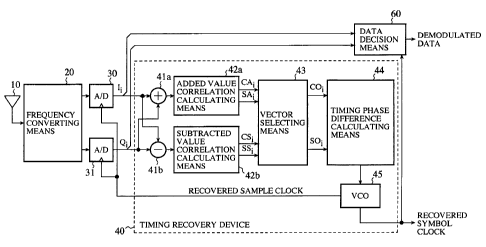
Fig. 1 is a block diagram illustrating the configuration of a
demodulator according to Embodiment 1. In Fig. 1, reference numeral 10
denotes an antenna for receiving a radio signal; 20 denotes frequency
converting means for frequency converting the radio signal received by the
antenna 10 to a base band signal; 30 and 31 denote A/D converters each for
sampling the base band signal frequency converted by the frequency
converting means 20 at a rate twice higher than a symbol rate for conversion
to a digital base band signal; 40 denotes a timing recovery device for
performing timing synchronization, using the digital base band signals
converted by the A/D converting means 30 and 31; and 60 denotes data
decision means which extracts Nyquist point data from the digital base band
signals through the use of a recovered symbol clock output from the timing
recovery device 40 and makes a decision on the extracted Nyquist point data.
In the timing recovery device 40, reference numeral 41 a denotes
adding means for adding together an in-phase component of the base band
signal and a quadrature component of the base band signal; 41b denotes
subtracting means for subtracting the in-phase component of the base band
signal and the quadrature component of the base band signal from each other;
CA 02371891 2001-08-16
28
42a denotes added value correlation calculating means for calculating the
correlation between the added signal and a 1/2 symbol frequency component;
42b denotes subtracted value correlation calculating means for calculating the
correlation between the subtracted signal and the 1/2 symbol frequency
component; 43 denotes vector selecting means which compares the magnitude
of the added value correlation signal and the magnitude of the subtracted
value correlation signal and selects the correlation signal of the larger
magnitude; 44 denotes timing phase difference calculating means for
calculating a timing phase difference, using the vector angle indicated by the
selected correlation signal; and 45 denotes a VCO (recovered sample clock
oscillating means) which controls the phases of a recovered sample clock and
the recovered symbol clock to reduce a timing error down to "0". Fig. 2 is a
block diagram of the vector selecting means 43, in which reference numeral
43a denotes maximum absolute value detecting means and 43b selecting
means.
Next, the operation of the demodulator according to Embodiment 1
will be described. The antenna 10 receives a burst signal of the RF band,
and the frequency converting means 20 frequency converts the RF-band burst
signal to a base band burst signal. This burst signal begins with a preamble
signal, which is followed by a significant data.
The preamble signal for use in Embodiment 1 may be either such a
signal (for example, "1101" pattern) as depicted in Fig. 18 or such a signal
(for example, "1001" pattern) as depicted in Fig. 25.
The AID converter 30 samples the in-phase component of the received
base band signal at time t=i+iT/2 (where i=1,2,3,..., i is a timing error
(-T/2<_i<T/2), and T is a symbol period), and outputs a sampled data
sequence I; (where i=1,2,3, . . . ). Similarly, the A/D converter 31 samples
the
CA 02371891 2001-08-16
29
quadrature component of the received base band signal at time t= i+iT/2, and
outputs a sampled received data sequence Q; (where I 1,2,3,...).
The timing recovery device 40 uses the received data sequence I;
(where i=1,2,3,...) and the received data sequence Q; (where I 1,2,3,...) to
detect a preamble signal (Ip;, Qp;) in the burst signal and calculate the
timing
error z through the use of the preamble signal, and effects phase control of
the
recovered sample clock and the recovered symbol clock to cancel the timing
error i. The recovered symbol clock is a clock of the symbol period
obtained by frequency dividing the recovered sample clock down to 1/2.
The data decision means 60 latches, by the recovered symbol clock,
data at the Nyquist points from significant random data sequences Id; and Qd;
(where i=1,2,3,...) following the preamble after the detection of the preamble
and cancellation of the timing error i by the timing recovery device 40. And
the data decision means uses the latched Nyquist point data to decide data,
and outputs demodulated data.
Next, the operation of the timing recovery device 40 will be described.
In the first place, the adding means 41 a adds together an in-phase component
I(t) and a quadrature component (Q(t) of the received signal, and outputs the
result of addition as an added signal. On the other hand, the subtracting
means 41b subtracts the in-phase component I(t) and quadrature component
Q(t) of the preamble signal from each other, and outputs the result of
subtraction as a subtracted signal. This subtraction may be either (I(t)-Q(t))
or (Q(t)-I(t)). Concretely, the adding means 41 a outputs the added signal
shown in Fig. 3 by the following equation (21 a).
A;=I;+Q; (21 a)
The subtracting means 41b outputs the subtracted signal shown in Fig. 4 by
the following equation (21 b).
CA 02371891 2001-08-16
(21b)
S.,--hQ;
With these simple adding means 41 a and subtracting means 41 b, it is
possible for the timing recovery device 40, in the case of receiving the
preamble signal (I; Ip;, Q,.--Qp;), to obtain either the added signal or
5 subtracted signal having a large 1/2 symbol frequency component,
irrespective of the value of the carrier phase 8c [deg].
For instance, when the carrier phase 8c [deg] is in the range of
(90<9c<180) or (270<0c<360) as shown in Fig. 25, the in-phase component
and quadrature component of the preamble signal are opposite in phase as
10 shown in Figs. 26 and 27; since the in-phase and quadrature components of
the preamble signal cancel each other as shown in Fig. 3, the amplitude of the
added signal is reduced, whereas the amplitude of the subtracted signal is
increased by the combining of the in-phase component and - (quadrature
component of the preamble signal as depicted in Fig. 4.
15 On the other hand, when the carrier phase 8c is in the range of
(0<8c<90) or (180<6c<270) as shown in Fig. 29, the in-phase component and
quadrature component of the preamble signal are in-phase with each other as
depicted in Figs. 3 and 31; hence, the amplitude of the subtracted signal is
reduced by canceling the in-phase and - (quadrature component) of the
20 preamble signal each other as shown in Fig 8, whereas the amplitude of the
added signal is increased by the combining of the in-phase component and
quadrature component of the preamble signal as shown in Fig. 7.
As described above, it is apparent that either of the subtracted signal in
Fig. 4 and the added signal in Fig. 7 contains a large 1/2 symbol frequency
25 (fs/2=1/(2T) component.
Similarly, in the case of receiving a preamble signal (for instance,
"1101" pattern) that effects an alternate transition between two adjacent
CA 02371891 2001-08-16
31
- - Nyquist points in the complex plane upon each occurrence of a symbol, too,
the timing recovery device 40 can obtain either one of the added signal and
the subtracted signal which has the 1/2 symbol frequency (fs/2=1/(2T))
component, no matter what value the carrier phase 8c may have. For
example, in the case of receiving the preamble signal having such a carrier
phase 9c as depicted in Fig. 18, the in-phase component and quadrature
component of the preamble signal are opposite in phase as shown in Fig. 5,
and it can be seen that the subtracted signal shown I Fig. 6 is larger in
amplitude than the added signal shown in Fig. 5 and is larger in the 1/2
symbol frequency (f~/2=1/(2T)) component.
The following description will be given of the operation of the present
invention in the case of receiving the preamble signal that performs an
alternate transition between two origin-symmetric Nyquist points in the
complex plane upon each occurrence of a symbol as shown in Fig. 25, but in
the case of receiving the preamble signal that performs an alternate
transition
between two adjacent Nyquist points in the complex plane upon each
occurrence of a symbol, too, the timing recovery scheme of Embodiment 1
permits implementation of the operation described below for the reasons (the
1/2 symbol frequency (f~2=1/(2T)) component can be obtained in either one
of the added signal and the subtracted signal) given above.
The added value correlation calculating means 42a calculates the
correlation of the added signal to the 1/2 symbol frequency component
exp[ jn(fs)t]. Concretely, the added value correlation calculating means
performs the following multiplications of a data sequence A; (where
i=1,2,3,...):
Ac.,--A;xcosni/2 (22a)
As; A;xsin~i/2 (22b)
CA 02371891 2001-08-16
32
The added value correlation calculating means averages the above
data sequences (Acl, As;), and outputs added correlation signals (CA;, SA;).
Since in the multiplications of Equations (22a) and (22b) cos~i/2=1, 0, -1, 0,
... and sinni/2=0, 1, 0, -1, ..., the above added value correlation signals
(CA;,
SA;) can easily be calculated. For instance, in the case of averaging the
above-mentioned data sequences over four symbols, the added value
correlation signals (CA;, SA;) can be given by the following equations.
Cr'i (~ ~+2+Ai+4 ~+6+~+8 ~+10+~+12 ~+14)/g (22c)
S"i-(~+1-~+3+~+5-~+7+~+9 ~+u+~+i3-~+is)/8 (22d)
Likewise, the subtracted value correlation calculating means 42b
calculates the correlation of the subtracted signal to the 1/2 symbol
frequency
component exp[ jn(fs)t]. Concretely, the subtracted value correlation
calculating means performs the following multiplications of a data sequence
S; (where i=1,2,3, . . . ).
Sc.,--S;xcos~i/2 (23a)
Ss~ S;xsin~i/2 (23b)
The subtracted value correlation calculating means averages the above
data sequences (Scl, Ss;), and outputs added correlation signals (CS;, SS;).
Since in the multiplications of Equations (23a) and (23b) cos~i/2=1, 0, -1, 0,
... and sin~i/2=0, l, 0, -1, ..., the above subtracted value correlation
signals
(CS;, SS;) can easily be calculated. For instance, in the case of averaging
the
above-mentioned data sequences over four symbols, the subtracted value
correlation signals (CS;, SS;) can be given by the following equations.
CS.,--(S; S;+2+S;+a S~+6+Sa+g S.+io+S~+i2 ;+i4)/8 (23c)
SS.,--(S;+1 S;+3+S;+5-Si+7+Si+9 S~+u+S.+i3-S;+is)/8 (23d)
For example, in the case where the carrier phase 8c [deg] is in the
range of (90<6c<180) or (270<6c<360) as shown in Fig. 25 at the time of
CA 02371891 2001-08-16
33
receiving the preamble signal, since the subtracted signal is larger in
amplitude than the added signal, the vector length indicated by the subtracted
correlation signals (CS;, SS;) is larger than the vector length indicated by
the
added value correlation signals (CA;, SA;) as depicted in Fig. 9. Fig. 9
shows the case where data is sampled at the timing shown in Figs. 3 and 4.
On the other hand, for example, when the carrier phase Ac [deg] is in
the range of (0<8c<90) or (180<9c<270) as shown in Fig. 15, since the added
signal is larger in amplitude than the subtracted signal, the vector length
indicated by the added value correlation signals (CA;, SA;) is larger than the
vector length indicated by the subtracted value correlation signals (CS;, SS;)
as depicted in Fig. 10. Fig. 10 shows the case where data is sampled at the
timing shown in Figs. 7 and 8.
Incidentally, at the time of receiving no signal (at the time of receiving
only noise in the absence of signals to be received) or during receiving a
significant data portion following the preamble, either of the added value
correlation signals (CA;, SA;) and the subtracted value correlation signals
(CS;,
SS;) indicates a small vector length since the 1/2 symbol frequency
component does not exist for a long time.
The vector selecting means 43 selects that one of the added value
correlation signals (CA;, SA;) and the subtracted value correlation signals
(CS;,
SS;) which indicate the larger vector length, and outputs them as selected
correlation signals (CO;, SO;). The operation of the vector selecting means
43 will be described with respect to Fig. 2. The maximum absolute value
detecting means 43a performs the same operation as in the case of the
conventional vector combining/selecting means 406 to detect the maximum
one of absolute values ~CA;~, (SA;~, ~CS;~ and ~SS;~ of the added value
correlation signals (CA;, SA;) and the subtracted value correlation signals
(CS;,
CA 02371891 2001-08-16
34
S S;).
The selecting means 43b selects the added value correlation signals
(CA;, SA;) when the maximum value detected by the maximum absolute
detecting means 43a is either one of ~CA;~ and ~SA;~, and selects the
subtracted
value correlation signals (CS;, SS;) when the maximum value is either one of
CS;~ and ~SS;~. The selected signals are output as the selected correlation
signals (CO;, SO;).
The operation of the vector selecting means 43 at the time of receiving
the preamble signal is such as described below. When the carrier phase 8c
[deg] is in the range of (90<Oc<180) or (270<8c<360) as shown in Fig. 25,
the vector length indicated by the subtracted value correlation signals (CS;,
SS;) is larger than the vector length indicated by the added value correlation
signals (CA;, SA;) as depicted in Fig. 9, and consequently, the vector
selecting
means 43 selects the subtracted value correlation signals (CS;, SS;), and
outputs selected correlation signals (CO;, SO;)= (CS;, SS;).
On the other hand, when the carrier phase Ac [deg] is in the range of
(0<6c<90) or (180<6c<270) as depicted in Fig. 29, the vector length indicated
by the added value correlation signals (CA;, SA;) is larger than the vector
length indicated by the subtracted value correlation signals (CS;, SS;) as
depicted in Fig. 10, and consequently, the vector selecting means 43 selects
the added value correlation signals (CA;, SA;), and outputs selected
correlation signals (CO;, SO;)= (CA;, SA;).
During receiving no signals (during receiving only noise in the
absence of signals to be received) or during receiving the significant data
portion following the preamble, either of the added value correlation signals
(CA;, SA;) and the subtracted value correlation signals (CS;, SS;) indicates a
small vector length, and the vector selecting means performs an operation of
CA 02371891 2001-08-16
randomly selecting either one of the added value correlation signals (CA;,
SA;) and the subtracted value correlation signals (CS;, SS;).
Next, the timing phase difference calculating means 44 performs the
following two processes at the same time. The one process is to calculate
5 the vector length V; of the selected correlation signals (CO;, SO;). The
vector length V; may be calculated by Equation (24a), but when it is desirable
to reduce the computational complexity, it may also be calculated by equation
(24b).
Vi (IC~iI2+ISO;IZ)1/2 (24a)
10 V.,--max(~CO;~, ~SO;~) (24b)
Incidentally, when it is desired to reduce absolute value converting
processing for obtaining ~CO;~ and ~SO;~, it is necessary only to selectively
use
~CA;~, SA;~, ~CS;~ and ~SS;~, calculated by the maximum absolute value
detecting means 43a, in accordance with the maximum value detected signal.
15 The other process is to calculate the vector angle
6o.,--tari 1(SO;/CO;) (25)
indicated by the selected correlation signals (CO;, SO;). Since 80; is a
timing
phase difference when normalized by the two-symbol period (2T), as is the
case with the aforementioned 6T, the timing phase 8r; [deg] when normalized
20 by the symbol period (T) is given by Equation (26).
8r.,--260; mod 360 (26)
While the timing recovery device 40 is receiving the preamble signal,
the vector length V; exhibits a large value, and the timing phase difference
0r;
[deg] becomes a certain value. For example, when such a preamble signal as
25 shown in Fig. 25 is sampled at the timing shown in Figs. 26 and 27, the
subtracted value correlation signals (CS;, SS;) shown in Fig. 9 are selected
by
the vector selecting means 43, and the vector length is V; and the vector
angle
CA 02371891 2001-08-16
36
is 80;. On the other hand, when such a preamble signal as shown in Fig. 29
is sampled at the same timing as mentioned above (that is, in the case of
Figs.
30 and 31), the added value correlation signals (CA;, SA;) shown in Fig. 10
are selected by the vector selecting means 43, and the vector length is V; and
the vector angle is 80;.
Incidentally, 60; in Fig. 9 and 80; in Fig. 10 differ by 180 [deg], but by
the processing of Equation (26), Or; derived from 60; in Fig. 9 and 8r;
derived
from 60; in Fig. 10 match each other.
On the other hand, while the timing recovery device 40 is receiving no
signals (receiving only noise in the absence of signals to be received) or
receiving the significant data portion following the preamble, the vector
length V; is small and the timing phase difference 6r; [deg] also becomes an
uncertain value. The certainty relationship between V; and Ar; is shown in
Fig. 11.
Thus, even in the case where the timing for receiving the burst signal
is unknown and the time of arrival of the preamble is unknown, the timing
error i can be calculated by the processing described below.
That is, the timing phase difference calculating means monitors the
vector length V;, and when V; is large, decides "receiving the preamble
signal" and latches the timing phase difference Br; [deg] at the timing shown
in Fig. 11. Since the latched timing phase difference 8s [deg] is, as is
evident from Fig. 11, the timing phase difference 8r; when V; is large, and
hence it is a certain value. The timing phase difference calculating means 44
calculates the timing error i by Equations (5a) and (5b) using the timing
phase difference 8s thus obtained, and supplies the VCO 45 of the following
stage with a control signal for canceling the timing error i.
Incidentally, in the case where the timing for receiving the burst signal
CA 02371891 2001-08-16
37
is know and the time of arrival of the preamble can be specified, the above-
described preamble detecting operation is unnecessary; hence, the timing
phase difference calculating means 403a in the prior art example can be used
in place of the timing phase difference calculating means 44. In this
instance,
the function of calculating the vector length V; and detecting its magnitude
is
unnecessary--this permits reduction of the scale of circuitry used.
The VCO 45 receives the control signal from the timing phase
difference calculating means 44, and controls the phases of the recovered
sample clock and the recovered symbol clock to reduce the timing error i
down to "0".
With its configuration and operations described above, the timing
recovery device 40 according to Embodiment 1 produces the effects listed
below.
First, since timing the recovery device has a simple construction
which performs the correlation calculation for a total of two signals, Le. the
signal having added together the in-phase and quadrature components of the
preamble signal and the signal having the two components subtracted from
each other and uses, for timing phase estimation, that one of the two
resulting
correlation values whose vector length is larger than the other, the circuit
scale and computational complexity of the timing recovery device of this
embodiment can be reduced as compared with the conventional timing
recovery devices 400 and 400a. For example, as compared with the timing
recovery device 400a, a high precision timing phase estimation can be
achieved by the short preamble, as in the case of the timing recovery device
400a, using the simple adding means 41 a, subtracting means 41 a and vector
selecting means 43 (Fig. 2) instead of using the vector combining/selecting
means 406 formed by complicated circuits (Figs. 23 and 24).
CA 02371891 2001-08-16
38
Second, the timing recovery device of this embodiment is effective for
the signal (for example, "1101" pattern) that effects alternate transition
between two adjacent Nyquist points in the complex plane for each symbol
and the "On" modulated signal (for example, "1001" pattern) that effects an
alternate transition between two origin-symmetric Nyquist points n the
complex plane for each symbol.
Third, since a high precision timing phase estimation using the
preamble and the preamble detection can simultaneously be performed by the
timing phase difference detecting means 44, normal timing phase control can
be achieved even when the timing for receiving the preamble is unknown.
Fourth, the above-mentioned 1 to 3 can be implemented a low
sampling rate of 2 [sample/symbol] as is the case with the prior art example.
Further, the demodulator using the timing recovery device of the
present invention realizes high-speed synchronization and high-speed
resynchronization with a small-scale circuitry and by a short preamble and
achieves an excellent BER (Bit Error Rate) in the significant data portion
following the preamble even in the case where the timing for receiving the
burst signal is unknown which is generated at turn-on or in reconnection after
returning from shadowing.
Incidentally, the timing recovery device 45b of Embodiment 1 is
applicable to systems using any modulation schemes (BPSK, QPSK,
n/4QPSK, OQPSK, FSK, and so on) as long as they are radio communication
systems using the preamble signal that effects an alternate transition between
two points in the complex plane for each symbol as well as the following two
preamble signals ((1) the preamble signal that effects an alternate transition
between two origin-symmetric Nyquist points in the complex plane for each
symbol, and (2) the preamble signal that effects an alternate transition
CA 02371891 2001-08-16
39
between two adjacent Nyquist points in the complex plane for each symbol).
Embodiment 2
Fig. 12 is a block diagram illustrating the configuration of a
demodulator according to Embodiment 2. In Fig. 12, reference numeral 10
denotes an antenna for receiving a radio signal; 20 denotes frequency
converting means for frequency converting the radio signal received by the
antenna 10 to a base band signal; 30 and 31 denote AJD converters each for
sampling the base band signal frequency converted by the frequency
converting means 20 at a rate twice higher than a symbol rate for conversion
to a digital base band signal; 40a denotes a timing recovery device for
performing timing synchronization, using the digital base band signals
converted by the A/D converting means 30 and 31; and 60 denotes data
decision means which extracts Nyquist point data from the digital base band
signals through the use of a recovered symbol clock output from the timing
recovery device 40 and makes a decision on the extracted Nyquist point data.
In the timing recovery device 40a, reference numeral 41 a denotes
adding means for adding together an in-phase component of the base band
signal and a quadrature component of the base band signal; 41b denotes
subtracting means for subtracting the in-phase component of the base band
signal and the quadrature component of the base band signal from each other;
42a denotes added value correlation calculating means for calculating the
correlation between the added signal and a 1/2 symbol frequency component;
42b denotes subtracted value correlation calculating means for calculating the
correlation between the subtracted signal and the 1/2 symbol frequency
component; and 43 denotes vector selecting means which compares the
magnitude of the added value correlation signal and the magnitude of the
CA 02371891 2001-08-16
subtracted value correlation signal and selects the correlation signal of the
larger magnitude.
Further, reference numeral 44 denotes timing phase difference
calculating means for calculating a timing phase difference, using the vector
5 angle indicated by the selected correlation signal; 45a denotes a VCO
(recovered sample clock oscillating means) which controls the phases of a
recovered sample clock and the recovered symbol clock to reduce a timing
error down to "0"; 46 denotes phase detecting means for detecting the timing
phase, using the base band signal sampled by the recovered sample clock; and
10 47 denotes phase detected signal averaging means for averaging phase
detected signals and for outputting the average as a phase lead/lag signal.
The operation of Embodiment 2 will be described below.
Embodiment 2 uses, in combination, such a conventional PLL timing
recovery device as disclosed, for example, in literature "A Study of QPSK
15 Timing Recovery Scheme Using Received Signal Phase Information" (written
by Fujimura, Journal of the Society of Electronics, Information and
Communication Engineers of Japan, VOL.J81-B-~no.6, pp.665-668, June
1998), and operates a PLL timing recovery device composed of the phase
detecting means 46, the phase detected signal averaging means 47 and the
20 VCO 45a even during the preamble detection and the timing error i
calculation by Embodiment 1.
The processing of the adding means 41 a and the subtracting means
41b to the timing phase difference calculating means 44 are the same as in
Embodiment 1, and upon detecting the preamble signal, a clock phase control
25 signal for canceling the timing error i, calculated at the same time as the
detection of the preamble signal, is provided as a first phase control signal
to
the VCO 45a.
CA 02371891 2001-08-16
41
Meanwhile, the phase detecting means 46 detects whether the timing
phase is leads or lags behind the received data (I;, Q;) based on, for
instance,
the scheme disclosed in the above-mentioned literature, and outputs a
detected "+1" if the timing phase leads the received data and "-1" if the
timing phase lags behind it.
The phase detected signal averaging means 47 averages such lead/lag
signals, for example, by a random walk filter, and outputs the average as a
second phase control signal. The VCO 45a controls the phases of the
recovered sample clock and the recovered symbol clock by the second phase
control signal, causing the timing phase to lead or lag, depending on whether
the second phase control signal is "positive" or "negative". The VCO 45a is
usually controlled by the second phase control signal, but when the preamble
is detected and the first phase control signal is input thereto, it controls
the
phases of the respective clocks, using the first phase control signal instead
of
using the second phase control signal.
A disadvantage of using only the second phase control signal is a large
amount of time needed to pull in the timing phase, because the lead/lag
control of the timing phase by the second phase control signal is effected,
for
instance, in steps of 1/16 symbol. On the contrary, an advantage of this
scheme is to enable the timing phase to be followed during receiving the
significant data portion following the preamble signal.
On the other hand, a disadvantage of using only the first phase control
lies in that during receiving the significant data portion following the
preamble signal the timing phase difference 8r; [deg] becomes uncertain and
cannot be used. On the contrary, an advantage of using the first phase
control signal alone is to permit high precision detection of the timing phase
difference by a short preamble signal as described previously in respect of
CA 02371891 2001-08-16
42
Embodiment 1.
Since Embodiment 2 uses both of the first phase control signal and the
second phase control signal, the above-mentioned two advantages compensate
for the above-mentioned two disadvantages, producing the following effect in
addition to those obtainable with Embodiment 1.
That is, this embodiment estimates and controls the timing phase with
high accuracy by a short preamble signal and, at the same time, enables the
timing phase to be followed even during reception of a significant random
data portion.
Incidentally, as is the case with Embodiment 1, the timing recovery
device 45c of Embodiment 2 is applicable to systems using any modulation
schemes (BPSK, QPSK, n/4QPSK, OQPSK, FSK, and so on) as long as they
are radio communication systems using the preamble signal that effects an
alternate transition between two points in the complex plane for each symbol
as well as the following two preamble signals ((1) the preamble signal that
effects an alternate transition between two origin-symmetric Nyquist points in
the complex plane for each symbol, and (2) the preamble signal that effects an
alternate transition between two adjacent Nyquist points in the complex plane
for each symbol).
Embodiment 3
Fig. 13 is a block diagram illustrating the configuration of a
demodulator according to Embodiment 3. In Fig. 13, reference numeral 10
denotes an antenna for receiving a radio signal; 20 denotes frequency
converting means for frequency converting the radio signal received by the
antenna 10 to a base band signal; 30 and 31 denote A/D converters each for
sampling the base band signal frequency converted by the frequency
converting means 20 at a rate twice higher than a symbol rate for conversion
CA 02371891 2001-08-16
43
to a digital base band signal; 40b denotes a timing recovery device for
performing timing synchronization, using the digital base band signals
converted by the A/D converting means 30 and 31; 70 denotes data
interpolating means for interpolating the digital base band signals sampled by
an asynchronous sample clock output from the timing recovery device 40b;
and 60a denotes data decision means which extracts Nyquist point data of the
interpolated base band signals output from the data interpolating means and
makes a decision on the extracted Nyquist point data.
In the timing recovery device 40b, reference numeral 41a denotes
adding means for adding together an in-phase component of the base band
signal and a quadrature component of the base band signal; 41b denotes
subtracting means for subtracting the in-phase component of the base band
signal and the quadrature component of the base band signal from each other;
42a denotes added value correlation calculating means for calculating the
correlation between the added signal and a 1/2 symbol frequency component;
42b denotes subtracted value correlation calculating means for calculating the
correlation between the subtracted signal and the 1/2 symbol frequency
component; 43 denotes vector selecting means which compares the magnitude
of the added value correlation signal and the magnitude of the subtracted
value correlation signal and selects the correlation signal of the larger
magnitude; 44 denotes timing phase difference calculating means for
calculating a timing phase difference, using the vector angle indicated by the
selected correlation signal; 48 denotes an oscillator (asynchronous sample
clock oscillating means) which outputs an asynchronous sample clock and an
asynchronous 1/2 symbol frequency component.
The operation of Embodiment 3 will be described below.
While Embodiment 1 has been described to use the feedback type
CA 02371891 2001-08-16
44
timing recovery device 40 which reduces the timing error i down to "0"
through phase control of the recovered sample clock and the recovered
symbol clock by the VCO 45, Embodiment 1 can be modified to use such a
feedforward type timing recovery device as indicated by the timing recovery
device 40b in Embodiment 3. That is, the VCO 45 is replaced with the
oscillator 48, then the data interpolating means 70 is added, and the
' processing of the data decision means 60 is switched to processing of the
data
decision means 60a.
The oscillator 48 outputs a free-running asynchronous sample clock of
a period twice higher than the symbol period. The A/D converters 30 and 31
sample data by the asynchronous sample clock at a rate of 2 [samplelsymbol].
The adding means 41a and the subtracting means 41b perform the addition
and subtraction of the asynchronously sampled received data (I;, Q;) as in
Embodiment 1. The added value correlation calculating means 42a
calculates the correlation between the added signal output from the adding
means 41a and the 1/2 symbol frequency component exp[ j~(fs)t] output
from the oscillator in the same manner as in Embodiment 1.
The subtracted value correlation calculating means 42b calculates the.
correlation between the subtracted signal output from the subtracting means
41b and the 1/2 symbol frequency component exp[ j~(fs)t] output from the
oscillator in the same manner as in Embodiment 1. The vector selecting
means 43 and the timing phase difference calculating means 44 perform the
same processing as in Embodiment 1 to calculate the timing error i.
The data interpolating means 70 interpolates the received data (I;, Q;)
obtained by asynchronous sampling at the rate of 2 [sample/symbol] to
generate received data having time resolution 1/16 the symbol period, for
instance, and outputs interpolated received data. The data decision means
' CA 02371891 2001-08-16
60a uses the timing error i information from the timing phase difference
calculating means 44 to extract a Nyquist point of the interpolated received
data, and outputs data of the extracted Nyquist point as demodulated data.
The feedforward type configuration of the timing recovery device of
5 Embodiment 3 described above produces the following effect in addition to
those obtainable with Embodiment 1.
That is, the use of the low-cost and small-sized oscillator 48 permits
further reduction of the cost and downsizing of the timing recovery device
40b.
10 Incidentally, as is the case with Embodiment 1, the timing recovery
device 45d of Embodiment 3 is applicable to systems using any modulation
schemes (BPSK, QPSK, ~/4QPSK, OQPSK, FSK, and so on) as long as they
are radio communication systems using the preamble signal that effects an
alternate transition between two points in the complex plane for each symbol
15 as well as the following two preamble signals ((1) the preamble signal that
effects an alternate transition between two origin-symmetric Nyquist points in
the complex plane for each symbol, and (2) the preamble signal that effects an
alternate transition between two adjacent Nyquist points in the complex plane
for each symbol).
20 Embodiment 4
Fig. 14 is a block diagram illustrating the configuration of a
demodulator according to Embodiment 4. In Fig. 14, reference numeral 10
denotes an antenna for receiving a radio signal; 20 denotes frequency
converting means for frequency converting the radio signal received by the
25 antenna 10 to a base band signal; 30 and 31 denote AID converters each for
sampling the base band signal frequency converted by the frequency
converting means 20 at a rate twice higher than a symbol rate for conversion
CA 02371891 2001-08-16
46
to a digital base band signal; 40c denotes a timing recovery device for
performing timing synchronization, using the digital base band signals
converted by the A/D converting means 30 and 31; and 60 denotes data
decision means which extracts Nyquist point data from the digital base band
signals and makes a decision on the extracted Nyquist point data.
In the timing recovery device 40b, reference numeral 41 a denotes
adding means for adding together an in-phase component of the base band
signal and a quadrature component of the base band signal; 41 b denotes
subtracting means for subtracting the in-phase component of the base band
signal and the quadrature component of the base band signal from each other;
42a denotes added value correlation calculating means for calculating the
correlation between the added signal and a 1/2 symbol frequency component;
42b denotes subtracted value correlation calculating means for calculating the
correlation between the subtracted signal and the 1/2 symbol frequency
component; and 43 denotes vector selecting means which compares the
magnitude of the added value correlation signal and the magnitude of the
subtracted value correlation signal and selects the correlation signal of the
larger magnitude.
Further, reference numeral 44a denotes timing phase difference
calculating means for calculating a timing phase difference, using the vector
angle indicated by averaged correlation signals; 45 denotes a VCO (recovered
sample clock oscillating means) which controls the phases of the recovered
sample clock and a recovered symbol clock; 49 denotes weighting means for
weighting the selected correlation signals according to the vector length
indicated by the selected correlation signals; 50 denotes weighted signal
averaging means for averaging the weighted correlation signals; 50a denotes a
first low-pass filter of a small time constant which is supplied with the
CA 02371891 2001-08-16
47
weighted correlation signals; and 50b denotes a second low-pass filter of a
large time constant which is supplied with the weighted correlation signals.
The operation of Embodiment 4 will be described below.
Embodiment 4 performs timing recovery through the use of not only the
preamble signal but also a random pattern signal following the preamble, and
realizes timing synchronization even during receiving the random pattern
signal, by a scheme different from that of Embodiment 2. Basically, this
embodiment extracts not only the preamble signal but also 1/2 symbol
frequency components present burst-wise at time intervals of several symbols
in the random pattern signal following the preamble, and averages them for
use in estimating the timing phase.
As described previously, the timing recovery device of each of
Embodiments 1 to 3 are effective for the following two preamble signals ((1)
the preamble signal that effects an alternate transition between two origin-
symmetric Nyquist points in the complex plane for each symbol, and (2) the
preamble signal that effects an alternate transition between two adjacent
Nyquist points in the complex plane for each symbol); the transition of such a
signal having the 1/2 symbol frequency component is also present during the
reception of the random pattern though it is as short as several symbols.
For example, in the case of the QPSK modulation system the 1/2
symbol frequency component is present in 8-bit data sequences of a total of
12 patterns listed below. The probability of occurrence of any one of them is
as low as 12/256=4.6%, but by detecting the 1/2 symbol frequency
components contained in these patterns and averaging them over a long
period of time, high precision timing phase estimation can be achieved even
during receiving the random pattern.
Pattern A: 11001100
CA 02371891 2001-08-16
48
Pattern B: 00110011
Pattern C: 01100110
Pattern D: 10011001
Pattern E: 11011101
Pattern F: 01110111
Pattern G: 11101110
Pattern H: 10111011
Pattern I: 01000100
Pattern J: 00010001
Pattern K: 10001000
Pattern L: 10001000
In Embodiment 4 of Fig. 14, the operations of the antenna 10 to the
vector selecting means are the same as in Embodiment 1 except one point.
This difference is to use a small number of pieces of data, about {4, 8, 12},
in
averaging the data sequences after multiplication by the added value
correlation calculating means 42a and the subtracted value correlation
calculating means 42b. For example, in the case of calculating the
correlation to any one of the 8-bit patterns A to L, the number of pieces of
data for averaging is eight consecutive pieces of data.
The weighting means 49 calculates the vector length VO; of the
selected correlation signals (CO;, SO;), then multiplies (CO;, SO;) by a
weighting value a corresponding to the magnitude of VO;, and outputs the
multiplied results as weighted correlation signals (CW;, SW;).
CW; aCO; (27a)
SW,.--aCO; (27b)
In this instance, the vector length VO; takes a very large value in the
case of receiving the above patterns A to D. It takes a large value in the
case
CA 02371891 2001-08-16
. - 49
of receiving the above patterns E to L. In the case of receiving other
patterns,
it takes a small value.
Hence, the weighting means 49 can extract only the correlation
information during the reception of the above patterns A to L by performing
the weighting based on the vector length VO; as indicated by Equations (27a)
and (27b). For example, in the case where VO; is detected as three-valued
using two threshold values and VO; has a very large value, set a=1. When
VO; has a large value, set a=1/2. Further, when VO; has a small value, set
a=0.
With such setting, the selected correlation signals (CO;, SO; having
uncertain timing phase information except the above patterns A to L will not
be output to the subsequent stage. Of the patterns A to L, the patterns A to
D contains many 1/2 symbol frequency components likely to have timing
phase information more certain than that of the patterns E to L; since heavy
weighting is carried out during receiving them, the 1/2 symbol frequency
components effective in the timing phase estimation are extracted efficiently.
The weighted signal averaging means 50 averages the weighted
correlation signals (CW;, SW;), and outputs the average values as averaged
weighted correlation signals (ECW;, ESW;). Since the weighted signal
averaging means 50 is supplied with heavily weighted (for example,
multiplied by "1") correlation signals (CW;, SW;) during the reception of the
preamble, accurate timing phase difference information can be obtained with
a small number of pieces of data. During receiving the preamble, it is
necessary to quickly cancel timing information on the burst signal previously
received and quickly acquire the timing information on the burst signal being
currently received. Hence, during receiving the preamble signal it is
necessary to perform the averaging with a small number of pieces of data.
CA 02371891 2001-08-16
- 50
On the other hand, during receiving significant random data, since the
weighted signal averaging means 50 is supplied with many lightly weighted
(for example, multiplied by "0") correlation signals (CW;, SW;), it is
necessary for obtaining accurate timing information to perform averaging
using a large number of pieces of data corresponding to tens to hundreds of
symbols.
To this end, the weighted signal averaging means 50 is provided with
the first low-pass filter 50a of a small time constant for the preamble signal
and the second low-pass filter 50b of a large time constant for significant
random data, and outputs output information (E1CW;, E1SW;) and (E2CW;,
E2SW;) from the both filters. For example, in the case of using two IIR
(Infinite Impulse Response) filters that bear a relationship of (3<~y (where
0<(3<1 and 0<~y<1), the first IIR (Infinite Impulse Response) filter performs
the following processing.
ElCW; ~3ECW;_1+CW; (28a)
~lsw; ~~sw;_1+sw; (2sb)
The second IIR (Infinite Impulse Response) filter performs the
following processing.
E2CW;=yECW;_1+CW; (29a)
E2SW;=yESW;_1+SW; (29b)
The timing phase difference calculating means 44a simultaneously
performs the preamble detection and the timing phase estimation using the
preamble by the following processing, and does the timing phase estimation
during receiving the significant random data as well.
The first processing is to calculate a normalized vector length V l;
indicated by the output (E1CW;, ElSW;) from the weighted signal averaging
means 50,
CA 02371891 2001-08-16
' S1
V1; ~(~1CW.,2+E1SW;2)u2 (30a)
and a normalized vector length V2; indicated by the output (E2CW;, E2SW;)
from the weighted signal averaging means 50,
V2;=y(E2CW;2+E2SW;2)v2 (30b)
The second processing is to latch a timing phase difference 8r,;
obtainable by the following equation when Vl; takes a large value (for
example, when V1; becomes larger than a certain threshold value Epl).
6r1; is the vector angle indicated by (E 1 CW;, E 1 SW;).
6r1.,--2Arl; mod 360 (31)
The third processing is to calculate a timing error i1 by Equations
(32a) and (32b) using the 6r1; latched timing phase difference a 1 s=6r1; and
supplies the VCO 45 of the following stage with a first control signal for
canceling the timing error i 1.
When 61 s> 180 [deg]
i 1=(81 s-360)T/360 (32a)
When A 1 s__<180 [deg]
i 1=(81 s)T/360 (32b)
In the fourth processing, after the phase control by the first control
signal (hereinafter referred to as first phase control) the clock phase
difference
becomes 0 [deg], and the timing phase difference information that is input to
the weighted signal averaging means 50 differs before and after the first
phase
control; hence, after the first phase control the weighted signal averaging
means 50 is controlled so that the vector angles indicated by the vectors
(EICW;, ElSW;) and (E2CW;, E2SW;) are set in the direction of 0 [deg].
E1CW; (E1CW;-,2+E1SW;_12)nz (33a)
E 1 SW,.--0 (33b)
E2CW.,--(E2CW;-12+E2SW;_l2)na (34a)
CA 02371891 2001-08-16
. - 52
E2SW; 0 (34b)
The fifth processing is to calculate a timing phase difference Ar2; by
the following equation.
9r2; is the vector angle indicated by (E2CW;, E2SW;).
Ar2.,--262; mod 360 (35)
In the sixth processing, when the following two conditions (Condition
A and Condition B) are satisfied after the first phase control, Ar2; is
latched as
timing phase difference information that is derived from a significant data
portion received signal, then the latched timing phase difference 02s=8r2; is
used to calculate a timing error i2 by Equations (36a) and (36b), and a second
control signal for canceling the timing error i2 is provided to the VC 45.
In this instance, Condition A is "the timing phase difference between
8r1; and 6r2; (for example, ~8r1; 8r2;~<_45 [deg]."
And Condition B is "V2; is large (for example, V2; is larger than a
threshold value Ep2)."
In the case of 92s>180 [deg]:
i2=(62s-360)T/360 (36a)
In the case of 62s_<180 [deg]:
i2=(92s)T/360 (36b)
In the seventh processing, after the phase control by the second control
signal (hereinafter referred to as second phase control), too, there is a
possibility that the timing phase difference information, which is input to
the
weighted signal averaging means 50, differs before and after the second phase
control; hence, after the second phase control the weighted signal averaging
means 50 is controlled by Equations (33a), (33b), (34a) and (34b) so that the
vector angles indicated by the vectors (E 1 CW;, E 1 SW;) and (E2CW;,
E2SW;) are set in the direction of 0 [deg].
CA 02371891 2001-08-16
. ~ 53
In the eighth processing, in the case of effecting third and subsequent
phase control during continuous reception of the significant random data, a
check is made to see if the above-said Condition B holds with a tens-of
symbols period after the second phase control, and if the condition holds, the
vector angle Ar2; indicated by (E2CW;, E2SW;) at that time is latched, then
the
latched timing phase difference 62s=6r2; is used to calculate the timing error
i2 by Equations {36a) and (36b), and the second control signal for canceling
the timing error i2 is applied to the VCO 45. At the same time, control by
Equations (33a), (33b), (34a) and (34b) is performed on the weighted signal
averaging means 50 to set the vector angles indicated by the vectors by
(EICW;, ElSW;) and (E2CW;, E2SW;) to 0 [deg].
In the ninth processing, if V 1; takes a large value again (for example,
if V1; becomes larger than the certain threshold value Epl) in this while, it
is
decided that the next burst signal has been received, return to the second
processing.
Fig. 15 shows an example of the operation of the timing phase
difference calculating means. Since the number of pieces of data used for
averaging by the weighted signal averaging means 50 is small; V 1; is large in
value only during receiving the preamble signal but small during receiving the
random data portion since the number of pieces of data used for averaging by
the weighted signal averaging means 50 is small. On the other hand, V2;
often takes a small value during receiving the preamble signal since the umber
of pieces of data used for averaging by the weighted signal averaging means
50 is large and information on the preceding burst signal may sometimes
remain, but during receiving the random data portion it is sufficiently large
in
value.
Accordingly, as depicted in Fig. 15, the first phase control is
CA 02371891 2001-08-16
54
performed by the first to fourth processing during receiving the preamble, and
the second and subsequent phase control is performed during receiving the
data portion.
Finally, the VCO 45 responds to the control signal from the timing
phase difference calculating means 44a to control the phases of the recovered
sample clock and the recovered symbol clock, reducing the timing error i
down to "0"
Thus, Embodiment 4 implements, as is the case with Embodiment 1,
high precision timing phase estimation in a short time during receiving these
preamble signals, while at the same time it achieves timing synchronization
even during receiving the random pattern signal by a scheme different from
that of Embodiment 2.
Incidentally, in the case where the timing for receiving the burst signal
is known and the time of arrival of the preamble can be specified, the above-
described processing can be substantially reduced. This involves the
modifications described below.
First, the weighted signal averaging means 50 is formed by the first lo-
pass filter 50a alone, and the time constant (for example, the forgetting
coefficient (3 in Equations (28a) and (28b)) of the first low-pass filter 50a
is
switched between a small value during receiving the preamble signal and a
large value during receiving the significant random data.
Second, since the preamble detecting operation is unnecessary, the
timing error i is calculated from the vector angle indicated by the output
(E1CW;, E1SW;) from the first low-pass filter 50a, using the timing phase
difference calculating means 403a of the prior art example instead of using
the timing phase difference calculating means 44a.
The above-mentioned two modifications permit substantial reduction
CA 02371891 2001-08-16
of the circuit scale.
Thus, the timing recovery device 40c in Embodiment 4 produces the
following effect in addition to those obtainable with Embodiment 1.
That is, the timing recovery device of this embodiment performs high
5 precision timing phase estimation and control with a short preamble signal,
while at the same time enables the timing phase to be followed even during
receiving the significant random data portion.
Incidentally, as is the case with Embodiment l, the timing recovery
device 45e of Embodiment 4 is applicable to systems using any modulation
10 schemes (BPSK, QPSK, ~/4QPSK, OQPSK, FSK, and so on) as long as they
are radio communication systems using the preamble signal that effects an
alternate transition between two points in the complex plane for each symbol
as well as the following two preamble signals ((1) the preamble signal that
effects an alternate transition between two origin-symmetric Nyquist points in
15 the complex plane for each symbol, and (2) the preamble signal that effects
an
alternate transition between two adjacent Nyquist points in the complex plane
for each symbol).
Embodiment 5
Fig. 16 is a block diagram illustrating the configuration of a
20 demodulator according to Embodiment 5. In Fig. 16, reference numeral 10
denotes an antenna for receiving a radio signal; 20 denotes frequency
converting means for frequency converting the radio signal received by the
antenna 10 to a base band signal; 30 and 31 denote A/D converters each for
sampling the base band signal frequency converted by the frequency
25 converting means 20 at a rate twice higher than a symbol rate for
conversion
to a digital base band signal; 40d denotes a timing recovery device for
performing timing synchronization, using the digital base band signals
CA 02371891 2001-08-16
, - 56
converted by the A/D converting means 30 and 31; 70 denotes data
interpolating means for interpolating the digital base band signals sampled by
an asynchronous sample clock output from the timing recovery device 40b;
and 60a denotes data decision means which extracts Nyquist point data from
the interpolated digital base band signals output from the data interpolating
means 70 and makes a decision on the extracted Nyquist point data.
In the timing recovery device 40d, reference numeral 41 a denotes
adding means for adding together an in-phase component of the base band
signal and a quadrature component of the base band signal; 41b denotes
subtracting means for subtracting the in-phase component of the base band
signal and the quadrature component of the base band signal from each other;
42a denotes added value correlation calculating means for calculating the
correlation between the added signal and a 1/2 symbol frequency component;
42b denotes subtracted value correlation calculating means for calculating the
correlation between the subtracted signal and the 1/2 symbol frequency
component; and 43 denotes vector selecting means which compares the
magnitude of the added value correlation signal and the magnitude of the
subtracted value correlation signal and selects the correlation signal of the
larger magnitude.
Further, reference numeral 44a denotes timing phase difference
calculating means for calculating a timing phase difference, using the vector
angle indicated by averaged correlation signals; 48 denotes an oscillator
(asynchronous sample clock oscillating means) which outputs an
asynchronous sample clock and an asynchronous 1/2 symbol frequency
component; 49 denotes weighting means for weighting the selected
correlation signals according to the vector length indicated by the selected
correlation signals; 50 denotes weighted signal averaging means for averaging
CA 02371891 2001-08-16
57
the weighted correlation signals; SOa denotes a first low-pass filter of a
small
time constant which is supplied with the weighted correlation signals; and SOb
denotes a second low-pass filter of a large time constant which is supplied
with the weighted correlation signals.
S The operation of Embodiment 5 will be described below.
While Embodiment 4 has been described to use the feedback type
timing recovery device 40c which reduces the timing error i down to "0"
through phase control of the recovered sample clock and the recovered
symbol clock by the VCO 45, the timing recovery device can be modified to
such a feedforward type timing recovery device as indicated by the timing
recovery device 40d in Embodiment 5. That is, the VCO 45 is replaced with
the oscillator 48, then the data interpolating means 70 is added, and the
processing of the data decision means 60 is switched to processing of the data
decision means 60a.
The oscillator 48 outputs a free-running asynchronous sample clock of
a period twice longer than the symbol period. The AID converters 30 and 31
sample data by the asynchronous sample clock at a rate of 2 [sample/symbol].
The adding means 41 a and the subtracting means 41 b perform the addition
and subtraction of the asynchronously sampled received data (I;, Q;) as in
Embodiment 1. The added value correlation calculating means 42a
calculates the correlation between the added signal output from the adding
means 41a and the 1/2 symbol frequency component exp[ jn(fs)t] output
from the oscillator in the same manner as in Embodiment 2.
The subtracted value correlation calculating means 42b calculates the
correlation between the subtracted signal output from the subtracting means
41b and the 1/2 symbol frequency component exp[ j~(fs)t] output from the
oscillator in the same manner as in Embodiment 2. The vector selecting
CA 02371891 2001-08-16
58
means 43 and the weighting means 50 perform the same processing as in
Embodiment 4 to calculate the timing error i.
The timing phase difference calculating means 44b performs the same
operation as does the timing phase difference calculating means 44a except
the point mentioned below. The following is a difference between the timing
phase difference calculating means 44b and the timing phase difference
calculating means 44a.
That is, since the timing phase difference calculating means 44b is the
feedforward type, the phase of the sample clock is not controlled. In
contrast to this, since the timing phase difference calculating means 44a is
the
feedback type, control by Equations (33a), (33b), (34a) and (34b) is
performed on the weighted signal averaging means 50, avoiding the necessity
for setting the vector angles indicated by (EICW;, EISW;) and (E2CW;,
E2SW;) to 0 [degJ.
The data interpolating means 70 interpolates the received data (I;, Q;)
obtained by asynchronous sampling at the rate of 2 [sample/symbolJ to
generate received data having time resolution 1/16 the symbol period, for
instance, and outputs interpolated received data.
The data decision means 60a uses the timing error i information from
the timing phase difference calculating means 44a to extract Nyquist point
data of the interpolated received data, and outputs the extracted Nyquist
point
data as demodulated data.
The feedforward 'type configuration of the timing recovery device of
Embodiment 5 described above produces the following effect in addition to
those obtainable with Embodiment 4.
That is, the use of the low-cost and small-sized oscillator 48 permits
further reduction of the cost and downsizing of the timing recovery device
CA 02371891 2001-08-16
59
40d.
Incidentally, as is the case with Embodiment 1, the timing recovery
device 45d of Embodiment 5 is applicable to systems using any modulation
schemes (BPSK, QPSK, ~/4QPSK, OQPSK, FSK, and so on) as long as they
are radio communication systems using the preamble signal that effects an
alternate transition between two points in the complex plane for each symbol
as well as the following two preamble signals ((1) the preamble signal that
effects an alternate transition between two origin-symmetric Nyquist points in
the complex plane for each symbol, and (2) the preamble signal that effects an
alternate transition between two adjacent Nyquist points in the complex plane
for each symbol).
INDUSTRIAL APPLICABILITY
The timing recovery device and the demodulator according to the
present invention are suitable for use in broadband radio communication
systems using a burst signal that begins with a preamble.