Note: Descriptions are shown in the official language in which they were submitted.
~~~'-~O-c~:V-I ~ . CA 02371945 2001-11-22
~.~~OC13~J
maven ~enttCHAPdI ~ GOUi,D (TUE) 6. 26' 01 14: 27/ST. 14: 25/N0. 426
0369660 P 6
1
A1VTENNA INTERFACE
FI>rLT3 OF THE INVENTION
The invention relates generally to s Time Division Duplex (1'DD) radio
transceiver, more particularly, to an antenna interface for a Time Division
Duplex
(TDD) radio transceiver.
BACx.~ROUND of T~r~ zNVErmoN
Traditionally, a radio transceiver requires both a Low Noise Amplifier
(LNA) for clear reception of a radio si~nat tr<<uistuitted to the transceiver
and a
Power Amplifier {PA) for transmitting a radio signal from the transceiver wer
long
distances.
In a Timc Division Duplex (TDD) transceiver, a transmitter and a receiver
are not utili:ced simultaneo~tsl3~. Typically, when the transmitter of a
transceiver is
on, the receiver of tha transceiver is off. T.ikewise, when the receiver is
on, the
transmitter is o~ For a typical TDD transceiver, to conserve power, the
rcce;vcr
Low Noise Amplifier (LNA) is powered down during a transnut cycle, and the
transmit power ampl it3er {PA) is powered down during a receive cycle.
In the past, a LNA and a PA in a transceiver have been discrete Componcnt~,
2U and they have been dt;signed independently from each other for their c~wn
optimum
performance. Therefore, a LNA and a YA have been t~.sing their own set of
different
matching comPonet~ts to interface with an antenna. For example, a LNA is
designed
to use its own set vf-matchin~ eompunents to match its input impedance to an
Futtenna impedance to obtain the maximum power' transfer fir a received Signal
ftUm
Em~fartgs;AMENDED SHEET
CA 02371945 2001-11-22 '.rSOGI3o~J~
FROM MERCIiANT & GOGLD (TDEj ~, 26,
01 14;27/ST.14.25/N0. 4260369660 P
la
an antenna to a LNA. On the other hand, a PA is designed to use its own set of
matching components to obtain a required output load impedance to maximize its
power amplification with maximum efficiency.
U.S. Patent No. 4.,055,807 relates to an antenna of a transceiver coupled
through low pass filter to the input port of a high pass fitter network.
Further, a
means for effectively switching an antenna between a receiver and transmitter,
which means also grovidcs an effective way to isolate the receiver from tire
transmitter when the sy stem is in the transmit mode.
EP 0 883 241 relates to an oscillating Stg11a1 that is ConlTOllcd in a
mutually
alternative first active component (; t ) and a second votive component (32),
which
both Cari be Set to sn active state by a first value of a control signal and
which are in
an inactive state with a second value of a control signal.
lrP 0 333 419 relates to a time division duplex transceiver where a reference
oscillator is a crystal-controlled oscillator (41 ) whose output is switched
as between
IS transnut mode ~rnd receive mode at a switch before being passed to the loop
phase
detector (28). The tr'msceiver is rapidly and repeatedly switcl~4d between a
transmit
and a receive mode.
Recently, as ljttebrated Circuit (IC) technologies improve, much effort has
been made to intea ate as many functional blocks as possible on a single chip
to
2U reduce its cost and size. Integration of a LNA and a IA onto a suiglc clop
often
requires careful attention. For example, if a LNA end a PA use different pins,
then
an antenna switch is required to toggle between a LNA input and a PA output in
a
TAD system. However, an antenna switch is costly and will still adversely
attenuate
EmvfanBS~AMENDED SHEET
CA 02371945 2001-11-22
WO 00/72457 PCT/US00/13606
2
the transmit and receive signals somewhat. In addition, a control circuit must
be
used to switch the antenna switch between a transmit cycle and a receive
cycle.
Also, a Balun (Balanced/LJnbalanced) circuit is used if a LNA and a PA are
differential. A Balun circuit and an impedance matching circuit are used in
both
transmit and receive paths. Furthermore, twice as much transceiver Integrated
Circuit (IC) package pins are needed to interface the transceiver with the
impedance
matching circuits for transmitting and receiving signals. The extra Balun
circuit, the
extra impedance matching circuit, and the extra transceiver IC package pins
make a
TDD transceiver system large in size and much more expensive.
It is with respect to these and other considerations that the present
invention
has been made.
SUMMARY OF THE INVENTION
In accordance with this invention, the above and other problems were solved
by providing an antenna interface that allows a transceiver to be attached to
an
antenna/filter without the need for an antenna switch.
In one embodiment, an antenna interface for a transceiver in accordance with
the principles of the present invention includes only one Balun circuit to
convert a
single-ended signal to/from differential signals, and only one impedance
matching
circuit to match an impedance at an output of the Balun circuit with an input
impedance of a Low Noise Amplifier (LNA) of a receiver and to provide an
output
load impedance required by a Power Amplifier (PA) of a transmitter, wherein
the
impedance matching circuit is coupled to both the LNA and the PA. The LNA and
the PA are based on CMOS technology and made within a single integrated
circuit.
In one embodiment, a Time Division Duplex (TDD) transceiver system in
accordance with the principles of the present invention includes an antenna
for
receiving and transmitting a signal; a bandpass filter to filter out noise
received from
the antenna; an antenna interface coupled between the bandpass filter and a
transceiver; and the transceiver including a receiver Low Noise Amplifier
(LNA) to
amplify a signal received from the bandpass filter and a transmit Power
Amplifier
(PA) to amplify a signal transmitted to the bandpass filter. The antenna
interface
includes only one Balun circuit, coupled to the bandpass filter, to convert a
single-
CA 02371945 2001-11-22
WO 00/72457 PCT/US00/13606
ended signal to/from differential signals; and only one impedance matching
circuit,
coupled to the Balun circuit and the transceiver, to match an impedance at an
output
of the Balun Circuit with an input impedance of a Low Noise Amplifier (LNA) of
a
receiver and to provide an output load impedance required by a Power Amplifier
(PA) of a transmitter, wherein the impedance matching circuit is coupled to
both the
LNA and the PA. The LNA and the PA are based on CMOS technology and made
within a single integrated circuit.
In another embodiment, an antenna interface between an antenna and a
transceiver in accordance with the principles of the present invention
includes only
one impedance matching circuit to match an antenna impedance with an input
impedance of a Low Noise Amplifier (LNA) of a receiver and to provide an
output
load impedance required by a Power Amplifier (PA) of a transmitter, wherein
the
impedance matching circuit is coupled to both the LNA and the PA. The LNA and
the PA are based on CMOS technology and made within a single integrated
circuit.
In another embodiment, a Time Division Duplex (TDD) transceiver system
in accordance with the principles of the present invention includes an antenna
for
receiving and transmitting a signal; a bandpass filter to filter out noise
received from
the antenna; an antenna interface coupled between the bandpass filter and a
transceiver; and the transceiver including a receiver Low Noise Amplifier
(LNA) to
amplify a signal received from the bandpass filter and a transmit Power
Amplifier
(PA) to amplify a signal transmitted to the bandpass filter. The antenna
interface
includes only one impedance matching circuit, coupled to bandpass filter and
the
transceiver, to match an impedance at an output of the bandpass filter with an
input
impedance of a Low Noise Amplifier (LNA) of a receiver and to provide an
output
load impedance required by a Power Amplifier (PA) of a transmitter, wherein
the
impedance matching circuit is coupled to both the LNA and the PA. The LNA and
the PA are based on CMOS technology and made within a single integrated
circuit.
These and various other features as well as advantages which characterize the
present invention will be apparent from a reading of the following detailed
description and a review of the associated drawings.
CA 02371945 2001-11-22
WO 00/72457 PCT/US00/13606
4
BRIEF DESCRIPTION OF THE DRAWINGS
Referring now to the drawings in which like reference numbers represent
corresponding parts throughout:
FIGURE 1 illustrates a typical antenna interface for a Time Division Duplex
(TDD) radio transceiver.
FIGURE 2 illustrates a block diagram of one embodiment of an antenna
interface for a Time Division Duplex (TDD) radio transceiver in accordance
with the
principles of the present invention.
FIGURE 3 illustrates a block diagram of another embodiment of an antenna
interface for a Time Division Duplex (TDD) radio transceiver in accordance
with the
principles of the present invention.
FIGURE 4 illustrates a circuit diagram of one embodiment of an impedance
matching circuit of an antenna interface in accordance with the principles of
the
present invention.
FIGURE 5 illustrates a flow chart of operations for receiving a signal in a
receive cycle.
FIGURE 6 illustrates a flow chart of operations for transmitting a signal in a
transmit cycle.
DETAILED DESCRIPTION
In the following description of the present invention, reference is made to
the
accompanying drawings which form a part hereof, and in which is shown by way
of
illustration specific embodiments in which the invention may be practiced. It
is
understood that other embodiments may be utilized and structural changes may
be
made without departing from the scope of the present invention.
The present invention allows for a transmitter and a receiver in a Time
Division Duplex (TDD) transceiver to be attached to an antenna/filter port
without
the need for an antenna switch. The present invention provides an antenna
interface
which combines a Low Noise Amplifier (LNA) input and a Power Amplifier (PA)
output into a single path so that external components, such as a Balun circuit
and an
impedance matching circuit, can be shared.
CA 02371945 2001-11-22
WO 00/72457 PCT/US00/13606
In a Time Division Duplex (TDD) transceiver system, a transmitter and a
receiver are not utilized simultaneously. In operation, when the transmitter
is on in a
transmit cycle, the receiver is off; and when the receiver is on in a receive
cycle, the
transmitter is off. In a transmit cycle, the receiver's Low Noise Amplifier
(LNA) is
5 powered down to conserve power. In a receive cycle, the transmitter's Power
Amplifier (PA) is powered down to conserve power.
One of the challenges in radio communication art is to find ways to get the
most power possible to generate and transmit a signal. Most transmitters are
preferably designed to provide maximum power output and efficiency into a 50-
ohm
load. Some antennas can provide a 50-ohm load to the transmitter over a wide
range
of frequencies. These antennas can be connected directly to the transmitters.
Other
antennas have impedances that vary widely with frequency and the surrounding
environment. In these cases, an antenna interface must be used. Also, a Low
Noise
Amplifier in a receiver requires impedance matching so as not to attenuate an
input
signal from the antenna.
FIGURE 1 illustrates a typical antenna interface 100 for a Time Division
Duplex (TDD) radio transceiver 102. The antenna interface 100 is coupled
between
a bandpass filter 104 and the transceiver 102. The bandpass filter 104 is
further
coupled to an antenna 106.
The antenna interface 100 includes an antenna switch 108 switching between
a transmit path 110 and a receive path 112. The antenna switch 108 is
controlled by
a receive/transmit control circuit 114. In a transmit cycle, the antenna
switch 108 is
switched to couple to the transmit path 110. In a receive cycle, the antenna
switch
110 is switched to couple to the receive path 112.
In the transmit path 110, the antenna interface 100 includes a Balun
(Balanced/CTnbalanced) circuit 116 which converts an unbalanced signal to
balanced
signals, i.e. converting differential signals to a single-ended signal. In
addition, an
impedance matching circuit 118 is coupled to the Balun circuit 116 to provide
the
optimum impedance at the PA output so that maximum power of the transmitted
signal from the transceiver 102 can be delivered to the antenna 106.
In the receive path 112, the antenna interface 100 includes a Balun
(Balanced/LJnbalanced) circuit 124 which converts the balanced signals to an
CA 02371945 2001-11-22
WO 00/72457 PCT/US00/13606
6
unbalanced signal, i.e. converting a single-ended signal to differential
signals. In
addition, an impedance matching circuit 126 is coupled to the Balun circuit
124 to
match impedance at the output of the Balun circuit 124 with an input impedance
of
the Low Noise Amplifier (LNA) 128 of the receiver 130. When impedance is
matched, maximum power of a signal is transferred from the antenna 106 to the
transceiver 102.
The receive/transmit control circuit 114 controls the transition between a
transmit cycle and a receive cycle such that the antenna switch toggles
between a
transmit cycle and a receive cycle. The transceiver 102 may include an enable
control circuit 132 which controls the power on/off for the PA 120 and the LNA
128.
As described above, the antenna switch 108 is costly and will still adversely
attenuate the transmit and receive signals somewhat. In addition, the
receive/transmit control circuit 114 must be used to switch the antenna switch
108
between a transmit cycle and a receive cycle. Further, two Balun
(Balanced/LJnbalanced) circuits and two impedance matching circuits have to be
used in the antenna interface 100 if the LNA and PA are differential.
Furthermore,
the pins for the transceiver 102 Integrated Circuit (IC) package are doubled,
for
example, four pins for balanced signals. The extra Balun circuit, the extra
impedance matching circuit, and the extra transceiver IC package pins increase
the
size and cost of the transceiver 102.
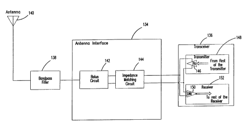
FIGURE 2 illustrates a block diagram of one embodiment of an antenna
interface 134 for a Time Division Duplex (TDD) radio transceiver 136 in
accordance
with the principles of the present invention. The antenna interface 134 is
coupled
between a bandpass filter 138 and the transceiver 136. The bandpass filter 138
is
further coupled to an antenna 140.
The antenna interface 134 includes a single Balun (Balanced/LTnbalanced)
circuit 142 which converts an unbalanced single-ended signal to balanced
differential signals in a receive cycle and converts balanced differential
signals to an
unbalanced single-ended signal in a transmit cycle. The antenna interface 134
also
includes an impedance matching circuit 144 coupled to the Balun circuit 142 to
match the impedance at the output of the Balun circuit 142 with an input
impedance
CA 02371945 2001-11-22
WO 00/72457 PCT/US00/13606
7
of a Low Noise Amplifier (LNA) 150 of a receiver 152 and to provide an output
load impedance required by a Power Amplifier (PA) 146 of a transmitter 148.
When
the impedance is matched at the antenna interface, maximum power of a
transmit/receive signal is transferred from/to the antenna 106 to/from the
transceiver
102.
The PA 146 and LNA 150 are based on CMOS technology and made within
a single integrated circuit (IC). The detailed circuit designs of the PA 146
and LNA
150, the bandpass filter 138, and the antenna 140 can be implemented in
various
ways known in the art and are not the focus of the present invention.
FIGURE 3 illustrates a block diagram of an alternative embodiment of an
antenna interface 154 for a Time Division Duplex (TDD) radio transceiver 156
in
accordance with the principles of the present invention. The transceiver 156
can be
the same as the transceiver 136 shown in FIGURE 2. Similarly, a bandpass
filter
158 and an antenna 160 can be the same as the bandpass filter 138 and the
antenna
140 shown in FIGURE 2. In FIGURE 3, the Balun circuit is not used. The signal
is
a single-ended unbalanced signal, i.e. the signal is not converted to balanced
differential signals. Accordingly, the antenna interface 154 includes only one
impedance matching circuit 162 which is coupled between the bandpass filter
158
and the transceiver 156. A PA 164 of a transmitter 166 and a LNA 168 of a
receiver
170 share one impedance matching circuit 162 in the antenna interface 154.
FIGURE 4 illustrates a circuit diagram of one embodiment of an impedance
matching circuit in an antenna interface in accordance with the principles of
the
present invention. As an example, the impedance matching circuit 162 of a
single-
ended unbalanced system as shown in FIGURE 3 is described herein. It is
appreciated that the impedance matching circuit can also be applied to a
balanced
system within the scope of the present invention.
In FIGURE 4, the impedance matching circuit 162 is made up of a
combination of inductance and capacitance to transform or match the impedance
at
the input (Rin) of the circuit 162 and the impedance at the output (Rout) of
the
circuit 162 in a receive cycle, and to transform or match the impedance at the
input
(Rout) of the circuit 162 and the impedance at the output (Rin) of the circuit
162 in a
transmit cycle. R1 represents the impedance of an antenna or antenna/filter.
R2
CA 02371945 2001-11-22
WO 00/72457 PCTNS00/13606
8
represents an input impedance of the LNA in a receive cycle since in the
receive
cycle, PA is off and provides high impedance in parallel to the input
impedance of
the LNA and therefore does not hinder the receive operation. On the other
hand, R2
represents an output load impedance of the PA in a transmit cycle since in the
transmit cycle, the LNA is off and provides high impedance in parallel to the
output
load impedance of the PA and therefore does not hinder the transmit operation.
In a receive cycle, the LNA is powered on, and its input impedance sets the
value of R2 to match Rout of the circuit 162 so that maximum received signal
power
can be transferred from the antenna interface to the LNA.
In a transmit cycle, the PA is powered on and delivers the power-amplified
signal onto R1 through the impedance matching circuit 162. The PA is designed
based on the value of Rout, i.e. R2 in the present invention.
The impedance matching circuit 162 is arranged to provide the desired R2 in
both a receive cycle and a transmit cycle. As an example, in a 900 MHz TDD
transceiver system, Rl is 50 Ohm, R2 is 100 Ohm, when CO is 8 pF, C1 is 3 pF,
C2
is 3.8 pF, L1 is 7 nH, and L2 is 2 nH. The resistance "looks in" from R1 is 50
Ohm
when R2 is 100 Ohm. R2 is 100 Ohm when R1 is 50 Ohm. It is appreciated that
other suitable specifications or combinations of Capacitance-Inductance can be
used
to provide the desired R2 in both a receive cycle and a transmit cycle.
FIGURE 5 illustrates a flow chart of operations for receiving a signal in a
receive cycle. In a receive cycle, an operational flow starts from an
operation 180 to
receive or detect a signal at an antenna 180. Then, the signal passes through
a
bandpass filter in operation 182. Next, the signal is converted to balanced
differential signals via a Balun circuit in operation 184. Then, the signals
are
delivered to an impedance matching circuit where the impedance is matched with
an
input impedance of the LNA in operation 186. Next, the signal is amplified by
the
LNA in operation 188 and sent to the rest of the receiver in operation 190.
Then, the
operational flow terminates.
FIGURE 6 illustrates a flow chart of operations for transmitting a signal in a
transmit cycle. In a transmit cycle, an operational flow starts from an
operation 192
to send a signal to the PA. Next, the signal is amplified by the PA in
operation 194.
Then, the PA delivers the amplified signal into the impedance matching circuit
?~_pc~_?~~01
~~SOp i 35~J:
11,~,~~ incdCHANT & G4IILD ' (TUE) 6. 26' Ol
14 28/ST. 14:25/N0. 4260369660 P 8
CA 02371945 2001-11-22
9
which provides the output load iuipedance that the PA requires in operation I
9~.
Next, the balanced differential signals ace converted to a single-ended
unbalanced
signal by the Balun circuit in operation 1 y8. Then, the signal passes through
the
bandpass filter in.operation ?00. Next, the signal is transmitted out via the
antenna
S in operation 202. Then, the operational flow terminates.
It is appreciated that in FIGURES 5 and 6, operations 184 and 198 can be
optional if a single-ended unbalanced signal is used.
It is also appreciated that the above described inventions van be applied to
other suitable devices, such as wireless modems or any other analogldigital
transceivers.
Further, it is noted that the Corms, such as antenna, antcntta interface,
etc., are
merely used to illustrate a specific TDD radio transceiver. It is appreciated
that
other suitable receivins/transmitting devices and interfaces can be used to
implement the present invention. .
In the preferred embodiments shown in F1GUR.ES 2-4, coupling lines or
wires arc used to connect various devices or components. It will be
appreciated to a
person skilled in the art that the coupling Lines or wires can be replaced by
infrared
or other suitable wirelass coupling devices to achieve the principles of the
present
invention.
It is to be understood that even though numerous characteristics and
advantages of various embodiments of me przsent i~,vc"t;on h~~e been set forth
in
the foregoing description, together with details of the structure and function
of
various embodiments of the invention. This disclosure is illustrative only.
and
changes may be made in detail within the principles of the present invention
to the
full extent indicated by the terms in which the appended claims axe exprcssad.
EmofangsZ qMENDED SHEET