Note: Descriptions are shown in the official language in which they were submitted.
CA 02372440 2001-10-29
POWER FEED AND HEAT DISSIPATING DEVICE FOR POWER SEMICONDUCTOR
DEVICES
TECHNICAL FIELD
The present invention relates to an electric supply and heat
radiating apparatus for a power semiconductor device in an electric
circuit having a plurality of power semiconductor devices, wherein
the power semiconductor devices are made to have a simplified
electric supply structure and a heat radiation action.
BACKGROUND ART
Generally, a control device to which a relatively large power
is supplied has an electric circuit provided with a plurality of
power semiconductor devices. For example, for the electric vehicle
receiving attention these days, an electric motor as a vehicle drive
source and its motor drive circuit, namely a device having a plurality
of power semiconductor devices, are housed in a metallic casing to
protect the motor and the circuit and mounted on the vehicle. This
casing comprises a metallic cylindrical case and cover made of
aluminum or the like and is assembled by housing the motor section
in the case, placing the cover in position and joining the case and
the cover with bolts.
The motor drive circuit mainly comprises power semiconductor
devices as the switching device for controlling switching the
electric supply to the motor coil at a high speed. And, when the
power semiconductor devices generate heat up to a rated temperature,
it is necessary to suppress or stop the output of the motor in order
to protect the circuit. Then, in order to avoid occurrence of such
1
CA 02372440 2001-10-29
a situation and to obtain a high power, it is inevitable t.o externally
release the heat of the power semiconductor devices to out of the
motor case.
Therefore, conventionally, the heat radiation metallic parts
provided on the power semiconductor devices are mounted on a heat
sink having a heat radiating action.
In such a conventional electric circuit, e. g. , FET, the drain
electrode and the heat radiation metallic part of the power
semiconductor device are electrically connected. And when a power
semiconductor device used on a different circuit section is mounted
on the same heat sink, it is necessary to electrically insulate the
respective power semiconductor devices from the heat sink.
And, when the electrical insulation is secured as described
above, the heat radiation property of the power semiconductor device
is degraded because when the electrical insulator has a high electric
resistance, it also has a high heat resistance.
When the power semiconductor device is soldered 'to a circuit
board to provide a circuit structure, the circuit is generally
connected to terminals on the circuit board for connecting to an
external circuit such as a power supply and a motor. But, the power
semiconductor device generally deals with a large current and
requires, for example, a structure or a process for forming a pattern
with copper foils having a large thickness on the circuit board,
to form the circuit board in a multilayered structure to use its
inner layer or to form a grommet terminal on the circuit board.
Therefore, the conventional circuit board has a complex structure
which is hard to be made small, and needs many parts and processes,
resulting in a high cost.
2
CA 02372440 2001-10-29
In view of the aforesaid problems, it is an object of the
invention to provide an electric supply and heat radiating apparatus
for a power semiconductor device which is mounted on a circuit board,
has a simplified electric supply structure for the power
semiconductor device and also a heat radiation action.
DISCLOSURE OF THE INVENTION
The invention recited in claim 1 is an electric supply and
heat radiating apparatus for a power semiconductor device in an
electric circuit using a plurality of power semiconductor devices,
characterized in that:
the power semiconductor devices are provided with heat radiation
metallic parts to which electrodes of the devices are electrically
connected within packages of the semiconductors;
among the plurality of power semiconductor devices, the heat
radiation metallic parts of those having the electrodes of the same
potential connected to the heat radiation metallic parts are
electrically connected and secured to a single radiator having
conductivity; and
the radiator is used as one connection terminal.
As described above, according to the apparatus of the
invention, the plurality of heat radiation metallic parts are
electrically connected to the single radiator, which is used as the
single connection terminal. Accordingly, the necessity of separate
wiring from the electrodes related to the plurality of heat radiation
metallic parts can be eliminated, and the electric supply structure
can be simplified.
Besides, the plurality of heat radiation metallic parts are
3
CA 02372440 2001-10-29
connected to the radiator without through an electric: insulator,
so that a heat resistance between the individual power semiconductor
devices and the radiator can be made small, and the heat radiation
of the power semiconductor devices can be enhanced.
The invention recited in claim 2 is the electric supply and
heat radiating apparatus for a power semiconductor device according
to claim 1, wherein the radiator is provided in a plurality of numbers
and electrically connected and fixed to a single conductive heat
radiating plate, and the heat radiating plate is used as one
connection terminal.
Thus, the plurality of radiators are electrically connected
to the heat radiating plate so to be used as a single connection
terminal, so that the aforesaid electric supply structure can be
made more simple. Since the plurality of radiators are additionally
connected to the heat radiating plate, the heat radiation property
of the power semiconductor devices can be enhanced further more.
The invention recited in claim 3 is the electric supply and
heat radiating apparatus for a power semiconductor device according
to claim 2, wherein the heat radiating plate is electrically
insulated and fixed to another radiator.
In the aforesaid structure, heat of the heat radiating plate
is released by another radiator, so that the heat radiation property
of the power semiconductor devices can be improved further more.
The invention recited in claim 4 is the electric supply and
heat radiating apparatus for a power semiconductor device according
to claim 1, wherein the radiator is electrically insulated and fixed
to another radiator.
In the aforesaid structure, heat of the radiator is released
4
CA 02372440 2001-10-29
by another radiator, so that the heat radiation property of the power
semiconductor devices can be improved further more.
The invention recited in claim 5 is the electric supply and
heat radiating apparatus for a power semiconductor device according
to claim 4, wherein fixing areas between the radiator and another
radiator are larger than the fixing areas between the radiator and
the heat radiation metallic parts.
The aforesaid structure further improves the heat radiation
property of the power semiconductor devices.
Specifically, when the radiator and another radiator are
electrically insulated, a heat resistance between them is increased,
but the present invention has determined the fixing areas between
the radiator and another radiator to be larger than those between
the radiator and the heat radiation metallic parts. Therefore, an
mount of heat conducted from the heat radiation metallic parts to
the radiator and an amount of heat conducted from the radiator to
another radiator can be secured in good balance. As a result, heat
of the power semiconductor devices can be radiated efficiently.
The invention recited in claim 6 is the electric supply and
heat radiating apparatus for a power semiconductor device according
to claim 4 or 5, wherein the radiator is a plate member and secured
to another radiator by screws.
By configuring as described above, the radiator can be
provided efficiently.
Especially, the radiator of the present invention is a plate
member and can be produced by stamping, and its production cost can
be reduced.
CA 02372440 2001-10-29
BRIEF DESCRIPTION OF THE DRAWINGS
Fig. 1 is a vertical sectional view showing an electric motor
provided with an electric supply and heat radiating apparatus for
power semiconductor devices according to an embodiment of the
invention.
Fig. 2 is a diagram showing an inverter circuit using the power
semiconductor device according to the embodiment of the invention.
Fig. 3 (1) shows an external perspective view of the power
semiconductor device and Fig. 3 (2) shows its circuit symbols
according to the embodiment of the invention.
Fig. 4 is an external perspective diagram showing a plurality
of power semiconductor devices mounted on a sub-heat sink according
to the embodiment of the invention.
Fig. 5 is an external perspective diagram showing a state that
a plurality of sub-heat sinks with a plurality of power semiconductor
devices mounted thereto are disposed on a circuit board.
Fig. 6 is an external perspective view partly broken in
section showing a state that the plurality of sub-heat sinks are
disposed on the circuit board, the sub-heat sinks being provided
with a heat radiating plate.
Fig. 7 is an external perspective view showing a circuit module
portion according to the embodiment of the invention.
Fig. 8 is an external perspective view showing a state that
the plurality of sub-heat sink are mounted on the circuit board,
the sub-heat sinks being provided with a heat radiating plate.
Fig. 9 is a vertical sectional view showing an electric supply
and heat radiating apparatus for the power semiconductor device
according to an embodiment of the invention.
6
CA 02372440 2001-10-29
Fig. 10 is an exploded perspective view showing the electric
supply and heat radiating apparatus for the power semiconductor
device according to the embodiment of the invention.
Fig. 11 is an external perspective view showing the power
semiconductor device according to the embodiment of the invention.
Fig. 12 is a plan view showing the power semiconductor devices
and the sub-heat sinks according to the embodiment of the invention.
Fig. 13 is a plan view showing the power semiconductor devices
and the circuit board according to the embodiment of the invention.
BEST MODE FOR CARRYING OOT THE INVENTION
Embodiments of the invention will be described with reference
to the accompanying drawings.
An embodiment refers to FET as an example of a power
semiconductor device, which has its electric supply and heat
radiating apparatus incorporated into an electric motor. First,
for convenience, the electric motor will be described.
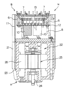
As shown in Fig. 1, an electric motor M comprises basically
a motor module A which accommodates mechanical elements of the motor,
and a circuit module B which accommodates electrical control
elements. In this embodiment, the motor is used as a drive source
for an electric vehicle.
The motor module A comprises a substantially cylindrical
hanger case 21 housing therein a motor body 22 and a resin block
23 with the motor body resin-sealed therein. The motor body 22
comprises a motor axis 24 rotatably supported with respect to the
hanger case 21, a rotor 25 fixed to the motor axis 24 and a stator
26 fixed to the hanger case 21.
7
CA 02372440 2001-10-29
The circuit module B comprises a metallic heat sink case 11
housing therein a circuit board 12 for controlling electric
conduction of the motor body 22, power semiconductor devices 1
mounted on the circuit board 12, sub-heat sinks 6 serving as a
radiator to be described afterward, a trident heat radiating plate
7, a condenser and other related component parts. Unillustrated
CPU and its related component parts for switching control of the
power semiconductor devices are also disposed within the heat sink
case 11.
The motor body 22 has its coil formed into three phases (U,
V and W phases) by arranging a winding at predetermined positions
of a core, and the coils of the respective phases are electrically
connected to the circuit board 12 on which a motor drive circuit
is mounted.
Fig. 2 shows an inverter circuit using the power semiconductor
devices 1. The plus pole and the minus pole of the connection
terminals are connected to a power supply, and connection terminals
U, V and W are connected to the motor.
The power semiconductor device 1 shown in Fig. 3 has a gate,
electrode 2, a drain electrode 3 and a source electrode 4, and a
heat radiation metallic part 5 electrically connected to the drain
electrode 3.
Three power semiconductor devices 1 shown at the upper section
of Fig. 2 can be attached directly to a single radiator because the
respective drain electrodes 3 have the same electric potential in
terms of the circuit.
With this embodiment, the three power semiconductor devices
1 are screwed to one single block sub-heat sink 6 as shown in Fig.
8
CA 02372440 2001-10-29
4. The sub-heat sink 6 is a conductive metallic member. By directly
fixing the three power semiconductor devices 1 to the sub-heat sink
6, the power semiconductor devices 1 are electrically connected with
the sub-heat sink 6.
Besides, the sub-heat sink 6 is used as a single connection
terminal. In this embodiment, a screw-in section is formed on the
back of the sub-heat sink 6, and a terminal 8a of a lead 8 is connected
to the screw-in section by a screw 9.
Thus, the device of this embodiment has the heat radiation
metallic parts 5 of the plurality of power semiconductor devices
1 electrically connected to the single sub-heat sink 6 and uses this
single sub-heat sink 6 as a single connection terminal. Thus, the
need for separate wiring from the drain electrode related to the
plurality of heat radiation metallic parts can be eliminated, and
an electric supply structure can be simplified.
This embodiment also has the plurality of heat radiation
metallic parts 5 connected to the sub-heat sink 6 without through
an electrical insulator, so that a heat resistance between each power
semiconductor device 1 and the sub-heat sink 6 can be lowered.
Accordingly, the heat radiation of the power semiconductor device
1 can be enhanced.
As shown in Fig. 5, the circuit board 12 is a circular plate
having a predetermined diameter. On the upper surface of the circuit
body 12, the sub-heat sinks 6 with the power semiconductor devices
1 tightly fixed thereto are mounted and the condensers 10 having
a large capacity mounted on the back surface.
Further, as shown in Fig. 6 and Fig. 7, the plurality of
sub-heat sinks 6 are fixed to projections 7a of the trident heat
9
CA 02372440 2001-10-29
radiating plate 7 which is another radiator. The sub-heat sinks
6 electrically connected and fixed to the heat radiating plate 7
have the same electrical potential in terms of the circuit.
The sub-heat sinks 6, each having a screw hole 6a on its top
surface, and the heat radiating plate 7 is fixed to the sub-heat
sinks 6 by unillusstrated screws through the screw holes 6a.
Thus, the plurality of sub-heat sinks 6 are electrically
connected to the heat radiating plate 7 and they are collectively
used as a single connection terminal. Therefore, a plurality of
electric supply structures can be integrated into one body, which
is made simple further more. Since the plurality of heat radiators
( sub-heat sinks 6 ~ are further connected to the heat radiating plate
7, a heat radiation property of the power semiconductor devices can
be enhanced further more.
The heat radiating plate 7 is forced to be in pressure contact
with the heat sink case 11 with an insulation sheet 13 interposed
between them as shown in Fig. 1 and Fig. 7. The insulation sheet
13 is disposed also on the top of the sub-heat sink 6, on which the
heat radiating plate 7 is not mounted, and forced to be in pressure
contact with the heat sink case 11. Radiator fins are formed on
the outer surface of the heat sink case 11.
As described above, the heat radiating plate 7 is forced to
be in pressure contact with the heat sink case 11, so that heat is
externally radiated from the heat radiating plate 7 through the heat
sink case 11. As a result, the heat radiation property of the power
semiconductor device 1 can be enhanced further more . The sub-heat
sinks 6 to which the heat radiating plate 7 is not mounted are also
forced to be in pressure contact with the heat sink case 11, so that
CA 02372440 2001-10-29
heat of the sub-heat sinks 6 is externally radiated through the heat
sink case 11, and the heat radiation property of the power
semiconductor device 1 is improved.
The heat radiating plate 7 and the sub-heat sinks 6 are
electrically insulated and fixed to the heat sink case 11, so that
a large current of the power semiconductor device 1 is not externally
scattered to be lost from the heat sink case 11. Thus, safety can
be secured.
The sub-heat sinks 6 having the same electrical potential in
terms of the circuit may be arranged on one side as shown in Fig.
8, and the heat radiating plate 7 may also be formed in a semicircle
form accordingly. The arrangement of the sub-heat sinks 6 is not
limited to the aforesaid embodiment but may be arranged in various
ways, such as in the form of a square.
It has been described in the above embodiment that the power
semiconductor device is incorporated in the electric motor. The
invention is not limited to the described embodiment but can also
be applied generally to other cases using the electric supply and
heat radiating apparatus for the power semiconductor device. FET
has been described as an example of the power semiconductor device
but not in a sense of limiting thereto. For example, there are also
transistors, diodes, thyristors, IGBT, SIT and the like, and they
can also be combined into a single package for application.
Another embodiment of the invention will be described with
reference to Fig. 9 to Fig. 13.
As shown in these drawings, the electric supply and heat
radiating apparatus of this embodiment have the sub-heat sinks 6
electrically insulated and fixed to the heat sink case 11.
11
CA 02372440 2001-10-29
Other basic structures are the same as in the aforesaid
embodiment; like reference numerals are used for like members, and
their descriptions will be omitted.
Specifically, the sub-heat sinks 6 of this embodiment are made
of a plate member which has on its one side the power semiconductor
devices 1 fixed thereto with screws, and fixed to the heat sink case
11 by screwing with an insulation sheet 13 interposed between its
other side and the heat sink case 11. The respective electrodes
2, 3, 4 of the power semiconductor device 1 have an ~ shape.
The sub-heat sinks 6 and the heat sink case 11 have a fixing
area larger than that between the sub-heat sinks 6 and the heat
radiation metallic parts 5.
To secure the sub-heat sinks 6 to the heat sink case 11 by
screws, screws 14 provided with an insulator or screws made of an
insulator are used, so as to assure the insulation between them.
In this embodiment, the heat radiation metallic parts 5 are
secured to the sub-heat sinks 6 by screws and the sub-heat sinks
6 are secured to the heat sink case 11 by screws, both in a direction
of the thickness of the sub-heat sinks 6. Therefore, to secure them
by screws, a tool can be inserted from the same direction, so that
the production process of the device can be simplified.
With the electric supply and heat radiating apparatus of the
power semiconductor device of this embodiment, heat of the sub-
heat sinks 6 is radiated by the heat sink case 11, and heat radiation
of the power semiconductor device 1 can be improved further more.
Even though the electrical insulation between the sub-heat
sinks 6 and the heat sink case 11 increases the heat resistance
between them, this embodiment has the fixing areas between the
12
CA 02372440 2001-10-29
sub-heat sinks 6 and the heat sink case 11 determined to be larger
than those between the sub-heat sinks 6 and the heat radiation
metallic parts 5. Therefore, an amount of heat conduction from the
heat radiation metallic parts 5 to the sub-heat sinks 6 and an amount
of heat conduction from the sub-heat sinks 6 to the heat sink case
11 can be secured in good balance. As a result, heat can be radiated
from the power semiconductor devices 1 efficiently.
Besides, the sub-heat sinks 6 are made of a plate member and
can be produced by stamping. Therefore, their production cost can
be reduced. And they can be provided efficiently by securing them
to the heat sink case 11 by screws. The flat form of the sub-heat
sinks 6 is determined appropriately by considering their fixing
areas to the heat sink case 11.
INDUSTRIAL APPLICABILITY
The present invention is directed to the electric supply and
heat radiating apparatus for the power semiconductor device in an
electic circuit using a plurality of power semiconductor devices,
wherein the electric supply structure of the power semiconductor
device is simplified and at the same time having the heat radiation
action. For example, it is suitably used as a motor drive circuit.
13