Note: Descriptions are shown in the official language in which they were submitted.
CA 02372551 2002-02-18
IMPROVED STRUCTURE AND METHOD FOR TESTING BOND
STRENGTH ANDIOR REMOVING INTEGRATED CIRCUIT DEVICES
BONDED TO SUBSTRATES
Field of the Invention
The present invention generally relates to packages of integrated circuit
devices attached to
substrates. More particularly, the invention relates to methods and structures
for facilitating the
removal of integrated circuit devices, microelectronic devices or die from
substrates and for
testing the integrity of the bonding between such devices and the substrate,
and preferably where
the integrated circuit device is a flip chip.
Background of the Invention
The use of flip chips and their connections to substrates is one of numerous
ways that
microelectronic devices may be connected to substrates. A flip chip is an
integrated circuit
device wherein the chip face providing interconnecting circuit contacts is
mounted face down.
The contacts are formed of a lead/tin alloy which when melted, will reflow and
maintain their
locations on the chip. These are commonly known as controlled collapse chip
connection (C4)
joints. When attaching flip chips to a module or substrate the chips are
positioned on
corresponding contact pads on the module and the module carrying the chips are
passed through
a furnace at a temperature sufficient to melt the lead/tin alloy of each C4
joint and reflow it to the
respective contact pads on the module. Upon cooling, the chips will be
physically and electrically
connected to the module. Because the flip chips with C4 joints permit area
connection or contacts
across the face area of the chip to the module, and not simply around the
periphery of the chip,
the chips can be spaced so closely together on the module that they resemble a
brick wall
arrangement in appearance. The spacing between chips could be in the order of
0.4mm spacing
or less. The chip and module structure is typically packaged by introducing
adhesive
encapsulating material in the space between the chip and the module. This
results in enhanced
physical protection for the contact structure as well as sealing the structure
to prevent damage
from moisture. This adhesive encapsulant in effect underfills the space
between the chip and the
CA9-2001-0070 1
CA 02372551 2002-02-18
substrate. The substrates or modules are typically comprised of appropriate
organic or ceramic
materials.
Situations arise where it may become important to test and verify the quality
of the bonding
between the chip and the substrate. In addition, there are situations where it
may be that a
particular chip has been determined to be defective and there is a requirement
to remove that
particular identified chip from the substrate and replace it with an
alternative chip. U.5. Patent
No. 6,117,695, which issued September 12, 2000 to Adrian S: Murphy et al, is
directed to An
Apparatus and Method for Testing a Flip Chip Integrated Circuit Package
Adhesive Layer. The
description provides for tension testing and assessing the integrity of the
bond formed by an
adhesive layer between the integrated circuit device and a plate, where the
plate may be a
substrate or a heat spreader. A lower portion of the apparatus for pulling the
integrated circuit
device is adhesively attached to a surface of the integrated circuit device
opposite the plate. The
further described apparatus is attached or connected to this lower portion
such that a force is
applied and the adhesive layer between the integrated circuit and the plate is
subjected to a force.
The apparatus provides for a variety of forces to be applied to the adhesive
layer which forces
include tension, a peel testing of the adhesive, or a shear testing of the
adhesive layer.
There is a need, however, for improved methods and apparatus for applying
forces to the
adhesive bonding between an integrated circuit device and a substrate which
are in essentially
pure tension in order to remove the chip from the substrate so as to minimize
damage to the
module and overcome damage to the base metal or inter-metallic and planar
layers of the
module.
Summary of the Invention
The present invention provides in one embodiment a microelectronic device or
die having a ball
and stud connector attached to a surface of the device opposite to the surface
which is intended to
be connected to a substrate. In other embodiments, the invention provides for
apparatus for
removing one or more die attached to a substrate, or assessing the integrity
of the bond between
each die and the substrate. Each die having a ball and stud connector attached
thereto is
CA9-2001-0070 2
CA 02372551 2002-02-18
positioned or secured in a holder. A mechanism clamped to the ball and stud
connector applies a
tensile force to the die such that the tensile force is exerted essentially
perpendicular to the
surface of the substrate to which the die is attached and this results from
the interaction of the
mechanism and the ball and stud connector. Without limiting the above or the
specification in
any manner, additional embodiments of the invention also provide for methods
of removing a
die from a substrate without significant damage to the die or the substrate or
for assessing the
integrity of the bond between a die and a substrate by attaching a ball and
stud connector to the
die. No application of heat is required. A mechanism is clamped to the ball
and stud connector
and upon activation the mechanism applies a tensile force to the die such that
the force is
caused to be essentially perpendicular to the surface of the substrate to
which the die is attached.
The perpendicular direction of the force results from the interaction of the
mechanism and the
ball. and stud connector. The combination of the die, substrate and connector
is held in such a
manner as to be moveable in the X and/or Y direction resulting from the
interaction of the
mechanism and the ball and stud connection.
The invention addresses the above identified and other problems associated
with the prior art by
providing in one aspect, a method for determining the integrity of the bond
between an
assembled integrated circuit device and a substrate. The method includes
attaching a connector
to a surface of the integrated circuit device, chip or die wherein said
connector includes a ball
and stud, and attaching a mechanism, for applying a tensile force to the bond,
to the ball of the
connector. The mechanism is caused to apply the force to the connector such
that the stud
limits the angle at which the force is exerted on the integrated circuit
device and substrate such
that the force is essentially perpendicular to the substrate. The tensile
strength of the bond is
then observed.
The invention also addresses these and other problems associated with the
prior art by providing
a method for removing an integrated circuit device, chip or die bonded to a
substrate which
includes attaching a connector to a surface of the integrated circuit device,
wherein said
connector includes a ball and stud, and attaching a mechanism, for applying a
tensile force to the
bond; to the ball of the connector. The mechanism is caused to apply the force
to the connector
CA9-2001-0070 3
CA 02372551 2002-02-18
such that the stud limits the angle at which the force is exerted on the
integrated circuit device
and substrate such that the force is essentially perpendicular to the
substrate. The integrated
circuit device is then separated from the substrate with minimal damage to the
substrate.
The invention also. addresses these and other problems associated with the
prior art by providing
an integrated circuit package which includes a die having an array of contacts
and a substrate
having an array of contacts such that the contacts of said die array are
interconnected to said
contacts on said substrate by a solder ball grid array and a ball and stud
device is attached to a
surface of the die opposite to said substrate.
The invention also addresses these and other problems associated with the
prior art by providing
an apparatus for removing an integrated circuit device interconnected to a
substrate by means of
a ball grid array of solder balls bonded to respective pads on the device and
substrate. The
apparatus comprises a ball and stud connector attached to a surface of the
integrated circuit
device and a holder positioning the substrate. A mechanism is clamped to the
ball of the
connector for providing a tensile pulling force. The mechanism and the
associated connector and
holder apply a tensile force to the integrated circuit device in a direction
which is essentially
perpendicular to the substrate sufficient to separate the integrated circuit
device from the
substrate with minimal damage to the substrate.
For a better understanding of the invention and of the advantages and
objectives obtained
through its use, reference should be made to the drawings and to the
accompanying descriptive
matter wherein there is described exemplary embodiments of the invention.
Brief Description of the Drawings
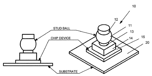
Figure 1 is an illustration of side and perspective views of a ball and stud
connecting device
shown bonded to a chip which in turn is bonded to a substrate, in accordance
with a preferred
embodiment of the invention;
CA9-2001-0070 4
CA 02372551 2002-02-18
Figure 2 shows the stud and ball connecting device of Figure 1 clamped in the
adjustable jaws of
a chuck assembly;
Figure 3 shows details of a holding fixture and a ball stud connecting device
connected to a chip
and a holding fixture for a mufti-chip array; and
Figure 4 is an illustration of one arrangement for permitting movement of the
holding fixture as
illustrated in Figure 3 in the X and Y directions.
Detailed Description of the Invention
Embodiments of the invention will be subsequently described which are
considered to provide
new and useful methods and apparatus for testing the integrity of the bond
between an integrated
circuit device, die or chip and a substrate as well as providing the
capability of removing the chip
from the substrate with minimal damage to the substrate. The invention results
in forces being
applied to the chip device which are essentially pure tension forces
perpendicular to the substrate
and whereby shear forces, or bending moment forces which could result in
damages to the chip
and/or the substrate, are avoided. This is achieved by the unique use of a
ball and stud or ball and
stem connector element. The unique ball and stud connector, when clamped by
the mating jaws
of a chuck assembly and pulled by a load cell and traction apparatus, allows
the chip package to
move slightly in the X and Y directions so as to result in essentially a pure
tensile force being
applied when the traction apparatus is activated. In effect, the novel ball
stud connector
arrangement allows the chip package to be self centred so that the tensile
force is essentially in
the Z direction perpendicular to the surface of the substrate to which the
chip is attached. This
results in minimal physical damage to the chip, the substrate, the surface of
the substrate; and its
various layers in the vicinity of the location where the chip is attached to
the substrate so that, for
example, another chip can be subsequently attached to replace the removed
chip. Where the
integrity or strength of the bond is merely being tested; the novel connector
resulting in the
tensile force on the chip, would ensure valid test results and minimize any
forces pulling on the
chip at a substantial angle from the vertical. It is noted that the usefulness
of the subject
CA9-2001-0070 5
CA 02372551 2002-02-18
invention does not require application of heat or the raising of the
temperature of the bond
between the chip and substrate:
Although particular details of the inventive concepts will be provided in the
description which
S follows, these details are considered to be those of preferred embodiments
of the invention and
thus, it is understood that the invention is not limited to these details. In
particular, in addition to
use of the invention involving flip chip technology, the invention could as
well be used with any
known arrangement where integrated circuit chips or die are attached to
substrates including thin
lead attachments. The particular substrate or module material need not be
limited in the sense
that organic, ceramic, plastic or any other material that is typically used
for such devices would
also provide useful results for the described inventive concepts: Within the
description of the
drawings, like reference numerals are used throughout the description and
drawings to illustrate
similar elements and components.
The novel ball stud connector used to cold pull and separate an integrated
circuit chip attached to
a substrate without the application of heat, will be described with reference
to Figure 1. The ball
stud connector is generally shown by reference 10 in association with an
assembled chip
substrate package. Chip device 15 is shown bonded to substrate 20 in any well
known manner
including, for example, an array of contact balls between the respective
mating contacts of chip
device 15 and substrate 20 and appropriate adhesive underfill between these
surfaces. Ball stud
connector 10 consists of a spherical portion 11, which will be clamped by jaws
of a chuck
assembly which is part of a load or traction mechanism or apparatus for
creating a pulling or
tensile force, as will be subsequently described, and an upstanding stud or
stem portion shown by
reference 12. Connector 10 includes element 13 and base element 14 of any
appropriate
configuration for positioning connector 10 on the upper surface of chip device
15 as shown. Ball
stud connector 10 is attached to the top surface of chip device 15 by applying
glue or adhesive
between the lower surface of base element 14 and the upper surface of chip
device 15. The
adhesive quality and strength of the glue that is used should in general be
stronger than the
strength of the attachment or bond between chip device 15 and substrate 20: In
actual use there is
minimal need for precise positioning of ball stud connector 10 on the surface
of chip 15. As will
CA9-2001-0070 6
CA 02372551 2002-02-18
be subsequently described, the invention provides for some variation in the X
and Y directions in
the positioning of the chip and substrate assembly so as to allow the ball
stud connector 10, chip
15 and substrate 20 to be properly positioned with respect to the traction
equipment or apparatus
and result in essentially tensile forces being applied. The shape of the
connector 10 will also tend
to compensate for any lack of precision. The area of contact of base 14 on the
upper surface of
chip 15 should be smaller than the surface area of chip 15, thereby preventing
the glue or
adhesive which is applied between base 14 and chip 15 from overflowing down
the sides of chip
15. Having the dimension of base l4 of connector 10 smaller than the surface
area of the chip 15
prevents adhesive from overflowing and further cementing chip 15 to substrate
20 which are
already interconnected. If this additional cementing was not prevented, the
force resulting from
the traction apparatus, for the cold pulling of chip 10 would be greater than
the force needed to
test the integrity of the bond or remove chip 1 S from substrate 20 as the
case may be, for a
chip/substrate assembly without the added cement and would in all likelihood,
cause mechanical
and physical damage to the surface of substrate 20, the contact bumps and/or
chip 15.
Connector 10 and all of its various portions and features as described can be
made integrally in
any known manner as by machining. The material for connector 10 could be any
suitable
material as would be apparent to one having ordinary skill in the material
science. Material
selected from brassy steel or plastic would be the preferred material.
Once connector 10 has been appropriately attached to chip 15 and the adhesive
cured, as is well
known, the jaws of an adjustable chuck assembly are clamped to connector 10 in
order to est the
integrity of the bond between chip 15 and substrate 20 or to remove chip 15
from substrate 20 as
the case may be, as is generally depicted in Figure 2. Figure 2 shows
connector 10, including
spherical portion or ball 11, base 14 and stud or stem 12, glued to the top
surface of chip 15 by
adhesive 16 and where chip 15 is bonded, as shown by reference 17 in a well
known manner as
by solder ball contacts and adhesive underfill, to substrate 20. The chuck
assembly is shown
generally by reference 25. Such chuck assembly 25 and load or traction
apparatus (not shown in
Figure 2) attached thereto for creating a pulling or tensile force is well
known and other than
particular details which will be subsequently described, need not be further
elaborated. Suitable
CA9-2001-0070 7
CA 02372551 2002-02-18
traction apparatus for applying a tensile force has been obtained from Instron
Corporation,
Canton, Massachusetts.
Adhesive material 16 need not be uniformly applied to the area between base 14
of connector
10 and chip 15 and in addition connector 10 need not be initially
perpendicular to substrate 15 as
some variation can be accommodated by the invention to result in essentially
tensile forces
being applied as will be subsequently described.
A commercially available adhesive that has been successfully used as adhesive
16 as part of
this invention is known by the trade name Loctite 495 or Superbonder 49950
available from
Loctite Corporation, Cleveland, Ohio. Other suitable adhesives may also be
available from
Loctite Corporation or other suppliers of adhesives such as 3M Company of
London, Canada.
The use of various materials for the ball and stud connector may require the
use of alternative
adhesives as would be readily apparent to those having ordinary skill in the
relevant materials
art. The adhesive per se is not considered to be an inventive aspect of the
present inventions.
Chuck assembly 25 includes a pair of jaws 26 adjustably positioned to clamp
upon ball 11 of
connector 10 . The shape of the inner surfaces of jaws 26 provides clamping
surfaces which are
complementary to and match the shape of the spherical ball 11. Once jaws 26
are physically
positioned around ball 11 of connector 10, a sleeve lock 27 of chuck assembly
25 is manually
slid downwardly into place by the operator. Sleeve 27 is designed with a
tapered surface which
force jaws 26 to close gradually around ball 11 of connector 10 when sleeve 27
is moved
downward, until sleeve 27 is completely in contact with jaws 26. When sleeve
27 is properly
positioned, jaws 26 are clamped onto ball 11 and cannot be opened.
Subsequently, after the
pulling operation has been completed by the traction apparatus and the chuck
assembly on ball
stud connector 10, jaws 26 can be manually opened by the operator by sliding
sleeve 27 upwards
out of engagement with the jaws 26. Stud connector 10 can then be disengaged
from jaws 26.
The significance of stud or stem element 12 of connector 10 will now be
described. As can be
seen from Figure 2, if connector 10 is not positioned in essentially a
vertical orientation with
CA9-2001-0070 8
CA 02372551 2002-02-18
respect to chip 15 or substrate 20 as a result of non-uniform application of
adhesive 16 for
example, stud 12 abuts against an inside surface of jaws 26 of the chuck
assembly 25. Thus,
when jaws 26 are properly assembled and clamped to ball stud connector 10
around ball 11, the
force exerted by chuck assembly 25 on connector IO and subsequently chip 15
which is attached
thereto is essentially in the vertical direction. If; during assembly of jaws
26 around ball 11 of
connector 10, connector 10 is at too great an angle to the vertical of the
horizontal plane of chip
or substrate 20; by virtue of stud 12 abutting the inside surface of jaws 26
the arrangement
will force ball 11 to slightly rotate within jaws 26 causing the attached chip
15 and substrate 20
to be similarly displaced in the X and Y plane. If there is too much
inclination of the connector
10 10 to the vertical when jaws 26 are attempted to be clamped on to ball 11,
sleeve lock 27 as
previously described will be prevented from sliding downwards over jaws 26 and
locking them
in place around ball 11. If jaws 26 are not appropriately locked in place,
they may slip on ball 11
of connector 10 or ball may actually slip out of jaws 26 and prevent proper
execution of the pull
test. Thus the interaction of the complementary shape of the inner surface of
jaws 26 to the ball
1 S 1 l and the physical abutting of stem 12 against an inner surface of j aws
26, will result in
essentially tension forces being exerted on chip 15 by the chuck assembly 25
combined with
attached load cell and traction apparatus. This will result in proper testing
of the joint integrity
between chip 15 and substrate 20 or, if desired, will result in chip 15 being
ultimately removed
from substrate 20 with minimal damage to chip 15 and substrate 20.
The description so far, with reference to Figures 1 and 2, has described the
assembly and theory
of implementation of the invention. In practice, however, the substrate with
one or more chips
attached thereto should be retained in a holding fixture in order to perform
the integrity test or
removal of the chip. Figure 3 illustrates the positioning of substrate 20 with
chip device 15
attached thereto and along with ball stud connector 10 mounted thereon in a
substrate holder 30.
Holder 30 is designed to have an appropriate shallow depression on the upper
surface thereof as
shown in order to accommodate the shape of substrate 20. Cover 31 having an
opening to
accommodate the shape of chip device 15 is placed to overlay substrate 20 as
shown and in
particular the portions of substrate 20 extending past chip 15 and maintains
substrate 20 within
the depression of holder 30. Cover 31 and substrate holder 30 are
appropriately clamped such
CA9-2001-0070 9
CA 02372551 2002-02-18
that the substrate 20 is held in place when a chuck assembly and associated
traction apparatus is
clamped to connector 10 by means of jaws 26 as previously described and a
tensile force is
applied to connector 10 and chip 15 so as to measure the integrity of the bond
between chip 15
and substrate 20 or to remove chip 15 from substrate 20 as the case may be.
Previously, the description has only pertained to testing or removing a single
chip from a
substrate. Where a substrate having multiple chips attached thereto is
involved, it may very well
be desirable to provide the capability of testing or removing any one or more
of the chips in such
a mufti-chip array. To accommodate this, holder 30 and cover 31 are designed
to have a number
of openings corresponding to the number of chips as shown by reference 32 in
Figure 3. In
Figure 3, only one connector 10 is illustrated as connected to a chip but it
could very well be that
each one of the other openings 33 in cover 31 for the chips, could accommodate
a similar
connector 10 attached thereto. Holder 32 would function in a comparable manner
to the holder
previously described for a single chip such that corresponding depressions
would exist in
substrate holder 30 to the openings 33. In operation, cover 31 is clamped to
the substrate holder
30 in a similar manner as had been previously described so that when a chuck
assembly is
attached to one or more of the connectors 10 positioned in openings 33 and
associated 'traction
apparatus is activated; the integrity of the joints between the respective
chips 15 and substrates
could be tested or alternatively the chips 15 could be removed from the
substrate 20 as a result
20 of the applied tensile forces. Chuck assembly 25 could be either moved over
the respective
openings 33 or the holder 32 could be moved under the chuck assembly 25 such
that the jaws 26
of the chuck assembly would in turn be clamped on to the respective connectors
10 in a similar
manner as had been previously described.
Reference had previously been made to the slight movement which may result in
the X andlor Y
directions of the chip/substrate package when connector 10 is not preferably
properly vertically
aligned and such movement results from the abutment of stem 12 against the
inner portion of
jaws 26. This resulting adjusting action can be accommodated by mounting
holder 30 on a
carriage that is movable in the X and Y directions. With reference to Figure
4, one exemplary
embodiment for accommodating this movement will be described. As shown, chuck
assembly
CA9-2001-0070 10
CA 02372551 2002-02-18
25 is clamped to connector 10 in a manner as previously described. Connector
10 is adhesivley
attached to a chip as previously described. Cover 31, having multiple windows
with one
connector 10 shown protruding from each window thereof, is shown clamped to
holder 30 and
thereby restraining the substrate upon which the chips are mounted as
previously described and
illustrated. Typical clamping means are as generally illustrated in Figure 4
but the details of such
are considered to be within the knowledge of one having ordinary skill in this
technology. Holder
30 and cover 31 are shown positioned on a holding plate 4U which in turn is
mounted on two
carriages 41 and 42 which permit movement of the substrate and connector
assembly in the X
and Y directions respectively. As a result, when ball 11 of connector 10 is
improperly oriented
within jaws 26, the resulting force of stud 12 on the inner surface of jaws 26
as previously
described, causes the package to move in either the X or Y directions or both,
in order to
properly orient ball 11 of connector 10 within jaws 26. This results in a self
centering movement
of connector 10 within jaws 26. When jaws 26 are properly clamped onto ball 11
of connector
10, thus resulting in connector 10 being essentially vertically aligned with
respect to the substrate
and essentially perpendicular thereto; all of the pulling forces from chuck
assembly 25 and
traction apparatus are essentially in the vertical direction and are
communicated through
connector 10 to the interface between chip 15 and substrate 20 without any
resulting shear forces
or forces in an inclined direction. As needed, for a mufti-chip array the
above process is repeated
for each chip and connector shown in Figure 4.
It is apparent in the above description that Garners 41 and 42 shauld be
freely moveable in the X
and Y directions respectively. When connector 10 and chuck assembly 25 are
initially manually
pre-aligned, chuck assembly 25 and stud 12 on connector 10 may not be
essentially
perpendicular to the surfaces of substrate 20 and chip 15. Jaws 26 of chuck
assembly 25 axe
clamped to ball 11 of connector 10 but since no pressure or forces are being
applied there is no
resulting movement: When the traction mechanism is activated and chuck
assembly 25 is caused
to move upward, jaws 26 clamped to ball 11 will start applying a force to stud
12, as had been
previously described, and this will cause carriers 41 and 42 to move in the X
and Y directions
respectively until the essentially perpendicular orientation of connector 10
is obtained.
Carriages 41 and 42 are intended to be freely moveable. If this is not the
case and a carriage is
CA9-2001-000 11
CA 02372551 2002-02-18
prevented from being moved in response to the forces on stud 12, chuck
assembly 25 may
apply an undesirable non-uniform force which is not essentially perpendicular
resulting in a
prying action on chip 15. This could result, for example, in a corner of chip
15 being
separated from substrate 20 and exposing chip 15 to failure as by fracture or
other physical and
mechanical damage.
As is well known, the integrity of the chip-to-substrate bond can be
determined by a
measurement of the pull strength per contact point of the connection resulting
from a meter
provided on the load cell. If desired, a microscopic verification and
examination may also be
conducted of the bond as it reaches the fracture point.
In order to facilitate the subsequent testing of the chip-to-substrate bond or
removing the chip
from the substrate altogether, as the case may be, during assembly and
packaging of the chip on
the substrate, a ball stud connector 10 as previously described, could be
attached to and form part
of the microelectronic device package. Similarly, in the fabrication of mufti-
chip substrate
packages, each one of the chips could be assembled with a ball stud connector
so that each chip
can be subsequently tested or removed as may be desirable without having to
add one or more
additional connectors.
Preferred embodiments of the present invention have been described hereinabove
by way of
example only and not of limitation such that those of ordinary skill in the
art of he exemplary
embodiments would readily appreciate that numerous modifications of detail may
be made to the
present invention, all coming within its spirit and scope. Various
alternatives and modifications
may be devised without departing from the invention. Accordingly, the present
invention is
intended to embrace all alternatives, modifications and variations which fall
within the scope of
the appended claims:
CA9-2001-0070 12