Note: Descriptions are shown in the official language in which they were submitted.
CA 02372598 2001-12-05
WO 01/78091 PCT/USO1/11027
MINIATURIZED AC/DC POWER SUPPLY AND BATTERY CHARGER
CROSS-REFERENCE TO RELATED APPLICATIONS
This application is a continuation-in-part of provisional patent applications
60/195034 filed April 6, 2000 and 60/196537, filed April 11, 2000, the entire
contents of
which are hereby incorporated by reference.
STATEMENT REGARDING FEDERALLY SPONSORED RESEARCH
Not Applicable
BACKGROUND OF THE INVENTION
This application related to miniaturized power supplies and battery
chargers. In particular this application discloses an inventive transformer
and inventive
control element which permit the manufacture of smaller and lower cost AC/DC
power
supplies and battery chargers.
The use of planar transformers is well known in the art. See for example
the following patents:
US 5502430
US 5754088;
US 5949321;
US 6069548;
US 6144276;
US 6208531.
Patents related to miniature transformers and miniature power supplies and
battery chargers are also lcnown in the art. See for example the following
patents:
US 5534839, and
US 6100664.
US 6208531 is related to a power converter having magnetically coupled
control.
None of the prior art provides a power supply/battery charger which has a
universal input which accepts a DC input of between 10-30 VDC or an AC input
of
1
CA 02372598 2001-12-05
WO 01/78091 PCT/USO1/11027
between 85VAC to 265VAC and between 50-60 Hz and provides a regulated DC
output
voltage or current; which utilizes a planar transformer; which provides a
programmable
control which allows the device to work with any battery chemistry, as well as
a variable
power source such as a solar cell; which eliminates the need for bulky hold up
capacitors;
which matches the impedance of the power source and the impedance of the Ioad,
and
which can be electrically isolated using magnetic isolation.
For the purpose of this disclosure, all US patents and patent applications
and all other publications referenced herein are incorporated herein by
reference in their
entirety.
SUMMARY OF THE INVENTION
Applicant has invented a miniature power supply and battery charger with
a universal input, so that it functions as a universal power module. The
inventive device
is connected to a power source, which can be AC or DC, which is connected to a
transformer, which consists of a primary coil, a secondary coil and a magnetic
core, the
secondary coil being configured to provide a regulated DC output voltage
and/or current.
A control circuit is electrically connected to the power source for
controlling first and
second FET's electrically connected to the control circuit, the first FET
being electrically
connected to an upper portion of the primary coil such that when the first FET
is activated
only the upper portion of the primary coil is utilized in the transformer, the
second FET
being electrically connected to a lower portion of the primary coil such that
when the
second FET is activated the entire primary coil is utilized in the
transformer. The control
circuit is configured to detect the input voltage of the power source and
above a
predetermined threshold voltage activate the second FET so that the power
module
operates as a high voltage input converter and below the predetermined
threshold voltage
activate the first FET so that the power module operates as a low voltage
input converter.
The inventive universal power module utilizes an inventive planar
transformer design which contributes to its miniature size. The inventive
planar
transformer includes a triple insulated primary winding formed into a planar
coil, and a
secondary winding formed on a printed circuit board (PCB). The triple
insulated primary
2
CA 02372598 2001-12-05
WO 01/78091 PCT/USO1/11027
winding and secondary winding are sandwiched between upper and lower magnetic
core
material, the triple insulated primary winding and secondary windings being in
physical
contact with each other. The use of the triple insulated primary winding
provides safety
isolation.
The control element includes a battery module circuit consisting of a
primary control circuit and a DC/DC converter for monitoring and maintaining
the chaxge
on a secondary battery. The primary control circuit regulates the input power
and is
connected
to a DC/DC converter which produces a regulated DC current used to charge the
battery.
The primary control circuit has three input lines for programming the primary
control
circuit, and the DC/DC converter having three input lines for programming the
DC/DC
converter. As few as a single wire could be used for programming, however
three lines
are standard using the JTAG standard.
The control circuit can also include a switch mode power supply which is
configured with an inventive circuit to traclc the voltage of a rectified
cycle of the AC
input source. This permits the elimination of bulky hold up capacitors,
thereby aiding in
the miniaturization of the device.
The control circuit can also include an inventive source impedance
matching circuit which includes a charger electrically connected to a power
source and a
battery, and a control circuit which ramps up the current from the power
source until the
load impedance of the charger is matched to the impedance of the power source.
The control circuit can also be programmably constructed and arranged so
that the DC output voltage and/or current of the universal power module may be
prograxnmably set by the user. This allows the device to be utilized with
different types of
batteries, on the fly.
Further miniaturization is permitted by using a high current low loss diode
connected to the secondary coil of the transformer. The high current low loss
diode
includes first and second high current, low on-resistance power MOSFETS
electrically
connected between an input and an output. A control circuit electrically
connected to the
first and second MOSFETS. which turns off the first and second MOSFETS when
the
voltage on the output is higher than the voltage on the input and which turns
on the first
3
CA 02372598 2001-12-05
WO 01/78091 PCT/USO1/11027
and second MOSFETS when the voltage on the input is higher than the voltage on
the
output.
The transformer utilized in the inventive device uses an inventive
construction to fiuther reduce the size. The transformer uses a bobbin having
opposite
sides. PCB support pins extend from each of the opposite sides of the bobbin,
first and
second windings axe located on each of the opposite sides of the bobbin, and a
core is
attached to the bobbin. Two PCB's are attached to the PCB support pins, one
PCB on
each side of the bobbin. The windings may be located either around the support
pins or
on the PCB's themselves.
The inventive universal power module can also be electrically isolated,
with the primary coil of the transformer being housed in a paddle and the
secondary coil
being housed in a mating receptacle. In this manner a load device is
electrically
connected to the secondary coil and electrically isolated from the power
source.
BRIEF DESCRIPTION OF THE SEVERAL VIEWS OF THE DRAWINGS
A detailed description of the invention is hereafter described with specific
reference being made to the drawings in which:
FIG. 1 is a circuit schematic of the inventive miniaturized AC/DC power
supply and battery charger;
FIG. 2 is an exploded perspective view of an inventive planar transformer
used in the inventive miniaturized AC/DC power supply and battery charger;
FIG. 3 is a perspective view of an alternate embodiment of the planar
transformer;
FIG. 4 is a side view of the alternate embodiment of FIG. 4;
FIG. 5 is a side view of an alternate embodiment of the embodiment of
FIG. 3;
FIG. 6 is a bloclc diagram showing an inventive battery module for use
with the circuit of FIG. l;
FIG. 7 is a circuit schematic of an inventive battery charger circuit which
allows for the elimination of bulky "hold up" capacitors in the circuit of
FIG. 1;
4
CA 02372598 2001-12-05
WO 01/78091 PCT/USO1/11027
FIG. 8 shows a rectified sine wave waveform produced by the circuit of
FIG. 7 without large capacitor 70;
FIG. 9 shows the waveform with large capacitor 70 in the circuit;
FIG. 10 shows the output of the SMPS of FIG. 7;
FIG. 11 is a circuit schematic for an inventive high current low loss diode
used in connection with the circuit of FIG. 1;
FIG. 12 is a circuit schematic for an inventive source impedance matching
battery charger used in connection with the circuit of FIG. l;
FIG. 13 is a graph showing the impedance matching of the circuit of FIG.
12;
FIG. 14 shows resistor programming for an inventive user programmable
power module;
FIG. 15 shows serial programming for an inventive user programmable
power module;
FIG. 16 shows PWM programming for an inventive user programmable
power module;
FIG. 17 shows a circuit schematic of an embodiment of the invention of
FIG. 1 with a magnetically coupled power inlet;
FIG. 18a-d show several views of the paddle and receptacle of the
inventive magnetically coupled power inlet of FIG. 17, and
FIG. 19 shows a circuit schematic of the mating receptacle circuitry.
DETAILED DESCRIPTION OF THE DRAWINGS
While this invention may be embodied in many different forms, there are
described in detail herein a specific preferred embodiment of the invention.
This
description is an exemplification of the principles of the invention and is
not intended to
limit the invention to the particular embodiment illustrated.
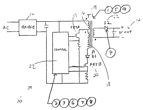
Referring now to FIG. 1, a circuit schematic of the inventive miniaturized
AC/DC power supply and battery charger is shown generally at 10 which allows
either a
DC input of between 10-30 VDC or an AC input of between 85VAC to 265VAC and
between 50-60 Hz and provides a regulated DC output voltage at 12. The power
supply
5
CA 02372598 2001-12-05
WO 01/78091 PCT/USO1/11027
and battery charger 10 utilizes a transformer with a tapped primary T1, shown
at 14. The
tap is arranged so that the upper portion of the primary coil 16 has the
correct number of
turns and magnetic performance to operate as a low voltage input DC/DC
converter using
FET A, shown at 17. The entire primary coil, consisting of both upper portion
16 and
lower portion 18 is constructed to have the correct number of turns and
magnetic
performance to operate as a high voltage input AC/DC converter using FET B,
shown at
20. When operated as a low voltage DC/DC converter, a high negative voltage is
induced
on the lower terminal of the transformer primary. Diode 19 blocks this high
negative
voltage from damaging FET B.
A control element 22 is connected to both FET A 17 and FET B 20. As
will be discussed further below, the programmability of the control element
22, along
with the dual fed primary configuration of the power transformer allows this
inventive
miniaturized AC/DC power supply and battery charger to convert a wide range of
input
voltage (10-30 VDC or an AC input of between 85VAC to 265VAC and between 50-60
Hz ) to a wide range of output voltage and current. The conversion can be
performed to
provide a constant output DC voltage, so the circuit can function as a power
supply;
programmable output current so the circuit can function as a battery charger,
or constant
power so the circuit can function as either a power supply or charger running
off of a solar
cell.
Referring now to FIG. 2, the tapped primary 14 of FIG. 1 is comprised of a
hybrid planar transformer shown generally at 30, in which 32 and 34 are two
halves of a
flat transformer core. The core material is ferrite or powdered iron for high
frequency
response. The primary winding is shown at 36 and is a flat coil with the wire
being triple
insulated with three layers of high voltage breakdown insulation material to
maintain a
high insulation between the primary winding 36 and the secondary winding 38.
The
primary coil is varnished or glued so that it will hold its wound coil flat
shape. The
secondary winding 38 is traced on the PCB layers and multiple secondary
windings 38
may be provided on mufti layer PCB's, as is well known in the art. The
advantage of
having only the secondary windings) on a PCB is the small size of the
transformer,
which the triple insulated primary winding provides for full safety isolation
between
primary and secondary without the need for creepage and clearance distances.
The use of
6
CA 02372598 2001-12-05
WO 01/78091 PCT/USO1/11027
the inventive planar transformer contributes to the miniaturization of the
device of FIG. 1.
Referring now to FIG.'S 3-5, several alternate embodiments of the planar
transformer are shown. FIG. 3 shows a bobbin 49 having PCB support pins 50 and
52
extending from each opposing face of the bobbin. The primary and secondary
windings
are wound around the bobbin, one to each side and the core of the transformer
is than
attached to the bobbin around the windings. Two PCB's 54 and 56 are soldered
to the
support pins 50 and 52. The circuitry associated with the primary winding is
located on
circuit board 54 and the circuitry associated with the secondary winding is
located on
circuit board 56. FIG. 5 shows a right angle embodiment of FIG. 3. Building
the
transformer between two PCB's reduces the overall package size and footprint,
contributing to the miniaturization of the device of FIG. 1.
Referring now to FIG. 6, a battery module is shown at 60, which is
incorporated as part of the control element 22 of FIG. 1. The battery module
is used as an
intelligent charger to monitor and maintain the charge on a secondary battery
and can be
programmed for any battery chemistry desired. A DC/DC converter 62 provides
power
from the primary control circuit to the battery for charging. A secondary
battery such as a
lead acid or cadmium sulfide battery is provided (not shown). Battery charge
requirements are either factory programmed or provided to the primary control
circuit via
a JTAG serial data stream; a serial EEPROM or a PWM signal. The DC/DC
converter is
then programmed to the desired output voltage and current using resistors, a
JTAG or
other serial data stream, serial EEPROM or a PWM signal. The power line,
battery and
DC/DC converter status and control are available through the serial data
stream.
Referring now to FIG.'S 7-10 a circuit is shown which allows for the
elimination of large and bulky hold-up capacitors) between the bridge 20 of
FIG. 1 and
the transformer 14. The circuit shown in FIG. 7 allows the control element 22
to follow
the rectified cycle of the AC line. The circuit of FIG. 7 is shown with prior
art hold-up
capacitors C 1 (large) 70 and C2 (small) 72, but it should be understood that
the use of the
circuit of FIG. 7 allows for the elimination of the large C1 capacitor. Hold-
up capacitors
C1 and C2 are well known in the art to function to "hold up" the DC voltage to
a nearly
constant value rather than rectified sine waves, shovcm in FIG. 8. This "hold
up" voltage
is shown in FIG. 9. The AC input source 74 is filtered with L1 76 and
rectified with
7
CA 02372598 2001-12-05
WO 01/78091 PCT/USO1/11027
either a half wave or full wave diode bridge 78 to produce a DC voltage
consisting of a
rectified sine waves, shown in FIG. 8. Without the hold up capacitor 70, the
voltage of
FIG. 8 drops nearly to zero at 60 or 120 Hz. This voltage is then applied to a
switch-
mode power supply (SMPS) 80. SMPS 80 chops the input voltage at a high rate,
such as
10 kHz or higher, and applies this chopped voltage (or in the dual case the
chopped
current) to the primary of the transformer 14. The secondary output of the
transformer is
a representation of the chopped current waveform from the primary. The
secondary
output of the transformer is rectified with diode 82 and filtered with
capacitor 84. This
voltage is then applied to the battery 86 to recharge it.
The SMPS 80 applies current pulses to the primary of the transformer as
shown in FIG. 10. Each pulse is much shorter in time duration as compared to
the 60 or
120 Hz input voltage. The SMPS can efficiently transfer power to the secondary
circuit
and therefore to the battery 86 by this high frequency switching action
through the
transformer. In addition, this circuit allows for the input and output
voltages to be
significantly different (e.g., a 120 VAC source can charge a 12 VDC battery)
by adjusting
the turns ratio of the transformer 14.
The SMPS 80 turns on or starts switching when the rectified DC input
voltage across 72 increases beyond a predetermined "turn on" voltage.
Conversely, when
the input voltage drops below the "turn on" voltage, the SMPS will stop
switching. When
the input voltage to SMPS 80 is between these two points is idle and is not
transferring
any power to the battery. The SMPS is turning off and on at either 60 or 120
Hz, which
results in the battery charge current being small bursts of current at either
60 or 120 Hz
rates.
A sample of the output voltage is measured with a feedback circuit 88 and
is used to control the operation of the SMPS, as is well known in the art.
When the
battery voltage indicates a full charge the SMPS is turned off until it is
necessary to
recharge the battery.
Because the battery offers low impedance to the output of the SMPS, is
possible to significantly reduce the value of C3 84 and allow averaging of
output current
pulses to occur in battery 86. Elimination of the bulky hold up capacitor 70,
which is
often the largest component in a battery charger contributes to a reduction in
the size and
8
CA 02372598 2001-12-05
WO 01/78091 PCT/USO1/11027
weight of the overall package and cost of the battery charger.
FIG. 11 is directed to a high current low loss diode circuit used at 82 in
FIG. 1, which provides for a very high efficiency and therefore smallest size
output diode.
The circuit of FIG. 11 allows for high currents to pass through transistors 90
and 92 with
much lower losses than if a conventional Schottlcey diode were used as 82 in
FIG. 1. Like
a semiconductor diode, current will flow only when the input voltage is
greater than the
output voltage, and not visa versa. Transistors 90 and 92 are high current,
low on-
resistance power MOSFETs. 94 is an isolated power MOSFET gate drive circuit,
such as
model HT0740. 96 is an operational amplifier IC that is capable of sensing
input voltages
above and beyond its power (VCC) terminals, such as the LT1782 available from
Linear
Technologies. The use of both transistors 90 and 92 shuts off current in both
directions
when these transistors are turned off. A simplified alternative version of
this circuit
would eliminate the gate 94 and transistor 92, which would then shut off
current in the
reverse direction, as in a conventional diode.
In the circuit, 98, 100 and 102 provide a Zener-regulated power source for
the operational amplifier. The voltage across 96 is 12 Volts. Op-amp 96 senses
the
voltage drop across 90 and 92 through resistors 104 and 106. If the voltage on
the output
108 is higher than the voltage on the input 110, then the output of the Op-amp
96 will go
to a low voltage (near to the voltage on the anode of D2). This will turn on
the PNP
transistor 112, causing current to flow through resistors 114 and 116 and
turning on the
NPN transistor 118. Transistors 112 and 118 act as level shifters giving a
ground
referenced output signal, which is further processed in the gate control logic
element 120
and is also used to turn off 90 and 92 through 122 and 94.
If the voltage on the input 110 is greater than the voltage on the output
108, then the output of Op-amp 96 will swing high, which will shut off 112,
which will in
turn shut off 118. This will cause 120 to turn on MOSFET gates 90 and 92 via
122 and
94. The use of the gate control logic 120 is not required by using the output
of either
transistors 112 or 118 to drive 94. As described above, elimination of the
gate also allows
the elimination of transistor 92.
Diode 124 provides protection of the input to 96 in the event the input
voltage to the MOSFET 90 is greater than the safe operating level of the Op-
amp 96.
9
CA 02372598 2001-12-05
WO 01/78091 PCT/USO1/11027
Depending on the operating levels of the circuit, diode 124 may not be
necessary.
The inventive circuit of FIG. 11 operates as an "ideal diode" where the
semiconductor diode behavior is achieved with little loss, and using this
diode as circuit
element 82 in FIG. 1 helps contribute to the overall miniaturization of the
inventive power
S supply.
Referring now to FIG.'S 12 and 13, an inventive source impedance
matching battery charger circuit is shown which is utilized in control 22 of
FIG. 1. This
circuit will allow either an AC/DC or DC/DC battery charger track the output
impedance
of a power source 150, such as a solar cell and provide charging of a battery
152 at a
voltage other than the optimum output voltage of the source 150. This circuit
also
provides battery charge management. A wide input voltage range power module is
used
as an intelligent charger 154, such as the circuit discussed above in
comlection with FIG.
6. Charger 154 monitors and maintains the charge on the secondary battery 152.
The
charger 154 can be programmed for any battery chemistry.
To use chaxger 154, the user provides a secondary battery 152, such as a
lead acid or cadmium sulfide battery. The battery charge requirements are
either factory
programmed or provided through a JTAG or other serial data stream, or a serial
EEPROM. Charger 154 then monitors the source voltage 150 and ramps up the
current
from the source until the load impedance of the source is matched, as shown in
FIG. 13.
Source 150, battery 152 and charging status and control are available through
the serial
data stream. This inventive circuit provides the advantage of complete,
programmable
battery charging for a portable or uninterruptable system from a variable
impedance
source such as a solar cell. The user need only add a secondary battery and
provide
programming information.
By using the inventive circuit of FIG. 12 in control 22 of FIG. 1, the
control element 22 can be programmed to present a matched impedance to the
power
source impedance. This increases the efficiency of the battery charging
process,
particularly when charging from high impedance sources such as solax cells.
Referring now to FIG's 14-16 show a universal input power module, such
as that shown in FIG. 1, that produces a DC output voltage that is
programmable by the
user. This capability could be programmed into control element 22 in a variety
of ways.
CA 02372598 2001-12-05
WO 01/78091 PCT/USO1/11027
In addition to the connections to the AC line, three pins are provided for
programming. A
microcontroller inside the power module monitors these pins for programming
information to set the output voltage and/or current of the module. FIG. 14
shows
resistance programming, in which resistor 200 is used to set current and
resistor 202 is
used to set voltage. FIG. 15 shows serial programming in which a serial data
stream
conforming to JTAG or other industry standard is used to set the voltage
and/or current.
FIG. 16 shows PWM programming in which a first PWM signal is used to set
voltage and
a second PW1VI signal is used to set current. A combination of the above
techniques could
also be used, for example a combination of resistors and PWM programming.
This inventive circuitry can be programmed to accommodate line drops,
temperature, time or humidity changes, or operational requirements such as
power level or
programming voltages. Since the settable voltages and current include zero,
this feature
can be used to turn the module on or off. Since both current and voltage are
settable, the
using assembly could throttle the power module to charge a battery using
either analog or
digital control. The use of this inventive programmable power module allows
changing
operation on the fly, such as accommodating several different types of
batteries.
Referring now to FIG.'S 17-19, an alternative embodiment of FIG. 1 is
disclosed in which the primary portion of the transformer and associated
circuitry is
enclosed in a paddle (see FIG. 18) and the secondary portion of the
transformer and
associated circuity is enclosed in a receptacle (see FIG. 18). This inventive
embodiement
allows the transfer of energy using magnetic coupling, which provides a fully
insulated
connector.
The primary portion of the transformer is housed in paddle 300, which is
designed to slide into slot 302 of receptacle 304. Paddle 302 removably locks
into the
receptacle 304 using detents 306 which lock with recesses 308. By magnetically
coupling
the paddle to the receptacle, the paddle can use any type of power source DC
or AC to
transfer energy to the load device, such as a battery connected to the
circuitry of the
receptacle 304 (see FIG. 19).
The above Examples and disclosure are intended to be illustrative and not
exhaustive. These examples and description will suggest many variations and
alternatives
to one of ordinary skill in this art. All these alternatives and variations
are intended to be
11
CA 02372598 2001-12-05
WO 01/78091 PCT/USO1/11027
included within the scope of the attached claims. Those familiar with the art
may
recognize other equivalents to the specific embodiments described herein which
equivalents are also intended to be encompassed by the claims attached hereto.
12