Note: Descriptions are shown in the official language in which they were submitted.
CA 02372707 2009-05-22
64371-434
-1-
NANOSCOPIC WIRE-BASED DEVICES, ARRAYS,
AND METHOD OF THEIR MANUFACTURE
Field of the Invention
The present invention relates generally to the controlled formation
and/or orientation of large molecules, such as nanotubes, on surfaces, and
more
particularly to formation of carbon nanotubes on surfaces for making
nanoscopic-
scale electronic devices such as memory arrays, configurable logic and other
computer elements.
Background of the Invention
During the past several decades there has been a nearly constant
exponential growth in the capabilities of silicon-based microelectronics
leading, for
example, to tremendous advances in our computational capabilities. Silicon-
based microelectronics, however, can be made only so small. That is, there is
a
size limitation smaller than which silicon-based microelectronics cannot be
fabricated. Specifically, the National Technology Roadmap for Semiconductors
(SEMATECH, Austin, 1997) suggest that silicon-based microelectronics, which
are typically said to follow "Moore's Law", will continue only to about the
year
2010. At this time, two factors are expected to bring Moore's scaling to an
end.
First, fundamental physical limitations will be reached for both device
elements
and wire interconnects that will prevent current designs from functioning
reliably.
Second, the concurrent exponential increase in fabrication (FAB) facility cost
is
expected to make it uneconomical to consider increasing integration levels
further
(using silicon technology) even if it is physically meaningful.
These factors, and the expected benefits that could be derived from
further dramatic increases in computational power in the relatively near
future,
have led many to consider new devices and computer architectures. In
particular,
there has been considerable interest in developing the concept of molecular
electronics. Molecular-based electronics can in
CA 02372707 2011-04-20
64371-434
2
principle overcome the fundamental physical and economic limitations of
silicon-based
microelectronics; it is physically possible to have single molecular devices.
For example, a
conformational change that varies the conjugation in a molecule could behave
as a switch or
rectifier.
Investigation has taken place into manipulation of molecules at surfaces for
electronic
applications. Liu, et al, in "Controlled Deposition of Individual Single-
Walled Carbon
Nanotubes on Chemically Functionalized Templates," Chem. Phys. Lett. 303
(1999) 125-129
report procedures for producing individual, short carbon nanotube segments and
for their
deposition on chemically functionalized nanolithographic templates.
Specifically, a patterned
self-assembled monolayer is formed on a surface and a carbon nanotube is
adsorbed onto the
surface in an orientation corresponding to the pattern. The authors also
describe connection
of an individual carbon nanotube between two electrodes.
Monolayers have been used to provide molecular electronic devices. Collier et
al.
describes the use of a Langmuir-Blodgett film of rotaxane molecules interposed
between
lithographically fabricated wires of micron-scale diameter (Science Vol. 285,
p. 391, 1999).
This system is useful for read-only memory devices, however, as the
configurable elements
involve irreversible oxidation of the rotaxane.
Other studies report a single carbon nanotube constructed as an electronic
switch
(Collins, et al., Science 278 (1997)100), and a room-temperature transistor
(Tans, et al.,
Nature 393 (1998) 49).
To date, there has been considerable progress in characterization of the
electrical
behavior of individual or small numbers of molecule devices. However, a
significant need
exists for improvement in molecule-scale electronics, especially for
integrating bistable and
switchable devices for high-density memory arrays.
Summary of the Invention
The present invention provides a series of nanoscopic-scale electronic
elements,
methods of making nanoscopic-scale electronic elements, and methods of use of
nanoscopic-
scale electronic elements.
In one aspect, the invention provides a nanoscopic-scale electronic device.
The
device is defined by an electrical crossbar array that includes at least one
nanoscopic wire.
CA 02372707 2001-11-01
WO 01/03208 PCT/US00/18138
- 3 -
The crossbar array can be of a variety of configurations such as a 1 x 8
array, 8 x 8 array, etc.
The array can include contact electrodes in electrical contact with various
wires, for example,
by covalent attachment. Crossbar arrays provided according to the invention
have densities
up to about 1012/cm2.
In another aspect the invention provides techniques for making nanoscopic-
scale
electronic devices. In one embodiment, the invention involves forming a
nanoscopic wire on
a surface in a pattern dictated by a chemically patterned surface. The
nanoscopic wire can be
a pre-formed wire, in which case the method involves applying the pre-formed
wire to the
surface in the pattern. Alternatively, the nanoscopic wire can be grown on the
surface in the
pattern. The chemically patterned surface can be patterned to direct assembly
or growth of
the nanoscopic wire in a predetermined orientation useful for a particular
electronic device.
In another embodiment the invention provides a method involving growing a
nanoscopic wire in the presence of an electric field. The field is of
intensity sufficient to
orient the growth of the wire. This method can, optionally, be used in
combination with a
method involving growing a nanoscopic wire on a self-assembled monolayer. In
all methods,
nanoscopic wire growth can be carried out via chemical vapor deposition (CVD).
In other embodiments, the invention provides a method involving forming a
nanoscopic wire on a surface in a pattern dictated by a mechanically patterned
surface or by
gas flow.
In another aspect, the invention provides methods of using electronic devices.
In one
aspect, a method of the invention involves providing a crossbar array
comprising at least two
wires in crossbar array orientation, where the wires are free of contact with
each other, and
bringing the wires into contact with each other. The wires are contacted at a
crossbar array
junction at which they are alternately brought into contact with each other
and released from
contact with each other. In one embodiment the wires are nanoscopic wires.
Another aspect of the present invention provides an article comprising a self-
assembled monolayer defining a delineated pattern. At least two crossed wires
are associated
with the self-assembled monolayer in which at least one of the wires is a
nanoscopic wire. In
another aspect, the invention provides an article comprising an electric
crossbar array
comprising at least two crossed wires defining a memory element able to be
switched
between at least two readable states. The device is free of auxiliary
circuitry other than the at
least two crossed wires defining the memory element.
CA 02372707 2012-07-12
. ,
64371-434
4
In another aspect, the present invention provides a method comprising
switching a memory element of a crossbar array between "on" and "off" states
by
alternatively biasing, at similar and opposite polarity, wires that cross the
array to
define the element.
In another aspect, the present invention provides an article comprising
an electrical crossbar array comprising at least two crossed nanoscopic wires
defining a memory element capable of being switched reversibly between at
least two
readable states.
In another aspect, the present invention provides an article comprising
an electrical crossbar array comprising at least two crossed nanoscopic wires
defining a memory element capable of being switched between at least two
readable
states. The memory element is non-volatile.
In another aspect, the present invention provides an article comprising
an electrical crossbar array comprising at least two crossed wires defining a
diode.
The device is free of auxiliary circuitry other than the at least two crossed
wires
defining the diode.
In another aspect, the present invention provides a method comprising
providing a mixture of metallic nanotubes in semiconducting nanotubes. The
method
also involves separating the metallic nanotubes from the semiconducting
nanotubes.
In all of the embodiments of the invention, preferred nanoscopic wires
are nanotubes.
In another aspect of the present invention, there is provided an article
comprising: an electrical crossbar array comprising a crossed conductor and
carbon
nanotube at a junction, wherein the carbon nanotube is constructed and
arranged to
be movable to a first position in direct physical contact with the conductor
by
application of dissimilar biasing electrical potential to the conductor and
the carbon
nanotube, and the carbon nanotube is constructed and arranged to be movable to
a
CA 02372707 2012-07-12
= =
64371-434
4a
second position not in direct physical contact with the conductor by
application of
similar biasing electrical potential to the conductor and the carbon nanotube.
According to another aspect of the present invention, there is provided
a method comprising: providing a crossbar array comprising a conductor and a
carbon nanotube in crossbar array orientation at a junction, the conductor and
the
carbon nanotube being free of physical contact with each other; and bringing
the
conductor and the carbon nanotube into physical contact with each other by
application of dissimilar biasing electrical potential to the conductor and
the carbon
nanotube.
According to still another aspect of the present invention, there is
provided an article comprising: a self-assembled monolayer defining a
delineated
pattern; and a crossed conductor and carbon nanotube associated with the self-
assembled monolayer, the carbon nanotube being constructed and arranged to be
movable to a first position in direct physical contact with the conductor by
application
of dissimilar biasing electrical potential to the conductor and the carbon
nanotube,
and the carbon nanotube is constructed and arranged to be movable to a second
position not in direct physical contact with the conductor by application of
similar
biasing electrical potential to the conductor and the carbon nanotube.
According to yet another aspect of the present invention, there is
provided an article comprising: an electrical crossbar array comprising a
crossed
conductor and carbon nanotube defining a memory element able to be switched
between at least two readable states, the carbon nanotube being constructed
and
arranged to be movable to a first position in direct physical contact with the
conductor
by application of dissimilar biasing electrical potential to the conductor and
the carbon
nanotube, and the carbon nanotube is constructed and arranged to be movable to
a
second position not in direct physical contact with the conductor by
application of
similar biasing electrical potential to the conductor and the carbon nanotube,
the
device free of means addressing the memory element to effect switching of the
memory element between the at least two states.
CA 02372707 2012-07-12
64371-434
4b
According to a further aspect of the present invention, there is provided
an article comprising: an electrical crossbar array comprising a crossed
conductor
and carbon nanotube defining a memory element able to be switched between at
least two readable states, the carbon nanotube being constructed and arranged
to be
movable to a first position in direct physical contact with the conductor by
application
of dissimilar biasing electrical potential to the conductor and the carbon
nanotube,
and the carbon nanotube is constructed and arranged to be movable to a second
position not in direct physical contact with the conductor by application of
similar
biasing electrical potential to the conductor and the carbon nanotube, the
device free
of auxiliary circuitry defining the memory element.
According to yet a further aspect of the present invention, there is
provided a method comprising: switching a memory element of a crossbar array
between "on" and "off' states by alternatively biasing, at similar and
opposite polarity,
a conductor and a carbon nanotube that cross in the array to define the
element,
wherein the carbon nanotube is constructed and arranged to be movable to a
first
position in direct physical contact with the conductor by application of
dissimilar
biasing electrical potential to the conductor and the carbon nanotube, and the
carbon
nanotube is constructed and arranged to be movable to a second position not in
direct physical contact with the conductor by application of similar biasing
electrical
potential to the conductor and the carbon nanotube.
According to yet a further aspect of the present invention, there is
provided an article comprising: an electrical crossbar array comprising a
crossed
conductor and carbon nanotube defining a memory element capable of being
switched reversibly between at least two readable states, the carbon nanotube
being
constructed and arranged to be movable to a first position in direct physical
contact
with the conductor by application of dissimilar biasing electrical potential
to the
conductor and the carbon nanotube, and the carbon nanotube is constructed and
arranged to be movable to a second position not in direct physical contact
with the
conductor by application of similar biasing electrical potential to the
conductor and the
carbon nanotube.
CA 02372707 2012-07-12
64371-434
4c
According to another aspect of the present invention, there is provided
an article comprising: an electrical crossbar array comprising a crossed
conductor
and carbon nanotube defining a memory element diode, the carbon nanotube being
constructed and arranged to be movable to a first position in direct physical
contact
with the conductor by application of dissimilar biasing electrical potential
to the
conductor and the carbon nanotube, and the carbon nanotube is constructed and
arranged to be movable to a second position not in direct physical contact
with the
conductor by application of similar biasing electrical potential to the
conductor and the
carbon nanotube, the device being free of auxiliary circuitry defining the
memory
element diode.
Other advantages, novel features, and objects of the invention will
become apparent from the following detailed description of the invention when
considered in conjunction with the accompany drawings, which are schematic and
which are not intended to be drawn to scale. In the figures, each identical or
nearly
identical component that is illustrated in various figures is represented by a
single
numeral. For purposes of clarity, not every component is labeled in every
figure, nor
is every component of each embodiment of the invention shown where
illustration is
not necessary to allow those of ordinary skill in the art to understand the
invention.
Brief Description of the Drawings
FIG. 1 illustrates, schematically, techniques for preparing a patterned
self-assembled monolayer on a surface, and use of the patterned monolayer for
growth of a nanoscopic wire;
FIG. 2 illustrates, schematically, use of patterned self-assembled
monolayers for formation of overlapping (intersecting) nanoscopic wires;
CA 02372707 2001-11-01
WO 01/03208 PCT/US00/18138
- 5 -
FIGs. 3A and 3B illustrate, schematically, catalytic growth of a two-
dimensional
nanoscopic wire array;
FIG. 4 illustrates, schematically and graphically, a bistable nanoscopic wire
junction
(memory element) and switching mechanism in terms of energy;
FIG. 5 illustrates, schematically and graphically, a bistable/nanoscopic wire
junction
(memory element) and switching mechanism in terms of energy;
FIGs. 6A, 6B, and 6C illustrate, schematically, bistable nanoscopic wire
crossbar
memory elements (crossbar junctions) in "on" and "off' states including three
arrangements
for provision of separate oppositely charged molecules;
FIG. 7 is a cut away schematic illustration of a crossbar array of the
invention.
FIG. 8 shows a schematic of a device of the invention featuring a crossbar
array;
FIG. 9A shows a top view of a crossbar array, illustrating cross talk;
FIG. 9B shows a top view of a crossbar array having diode junctions featuring
intrinsic rectifying behavior;
FIG. 10A shows a schematic of an article having parallel trenches and catalyst
nanoparticles for the production of crossed wires;
FIG. 10B shows a device having a crossbar array of nanowires in parallel
trenches
crossed by nanowires positioned over the trenches;
FIG. 11 shows plots of energy, ET for a single 20 nm device as a function of
separation at a junction;
FIG. 12 shows calculated structures of single wall nanotubes (SWNTs) in the
off and
on states for an initial separation of 2 nm;
FIG. 13 shows a plot of a calculated range of initial separations for a range
of device
sizes which yield bistable devices for a hard material such as silicon;
FIG. 14 shows a plot of a calculated range of initial separations for a range
of device
sizes which yield bistable devices for soft organic materials;
FIG. 15 shows calculations of ET for switching a 20 nm device on (FIG. 15A)
and off
(FIG. 15B);
FIG. 16A shows current-voltage (I-V) measurements made on lower (bound) and
upper (supported) nanotubes of a typical device showing ohmic behavior with
resistances of
11 and 58 k0;
CA 02372707 2001-11-01
WO 01/03208 PCT/US00/18138
- 6 -
FIG. 16B shows current-voltage (I-V) measurements made on lower (bound) and
upper (supported) nanotubes of a typical device showing ohmic behavior with
resistance of
112 k; and
FIG. 17 shows a plot of device state (on) and (off) vs. resistance.
Detailed Description of the Invention
The present invention provides a series of techniques and devices involving
nanoscopic-scale wires, also referred to herein as "nanoscopic wires".
"Nanoscopic-scale" or
"nano" is meant to include elements of widths or diameters of less than 1 pun.
Nanotubes are
used as one example of small wires for use in the invention and, in preferred
embodiments,
devices of the invention include wires of scale commensurate with nanotubes. A
"wire"
refers to any material having a conductivity of any semiconductor or any
metal.
One significant aspect of the invention involves electronic memory elements in
which
crossbar junctions (the intersections of crossed wires) are defined by at
least one nanoscopic-
scale wire. These crossbar junctions themselves can serve as both diode or
memory elements
of the device and as elements for switching between different states ("on" and
"off' states).
That is, a crossbar array device is provided in which one or more, preferably
all, elements are
free of auxiliary circuitry defining the elements. Current silicon based
devices require a
transistor and capacitor to store a bit in dynamic RAM, or four to six
transistors are required
to store a bit in static RAM. The present device is free of auxiliary
circuitry, such as
transistors and capacitors, addressing the elements to switch them between
states. This is
described more fully below. Of course, "free of auxiliary circuitry defining
the elements"
does not encompass electrodes and power sources or other macroscopic elements
required to
operate the device which are outside the nanoscopic memory element array.
In all of the exemplary embodiments described herein, circuitry including at
least one
nanoscopic-scale wire is described. Nanotubes, in particular carbon nanotubes,
are primarily
described and shown as examples of nanoscopic-scale wires. While nanotubes,
and in
particular carbon nanotubes, are preferred for use in the invention, any
nanoscopic-scale
wires can be used, including nanoscopic wires such as nanorods, nanowires,
organic and
inorganic conductive and semiconducting polymers, and the like. Other
conductive or
semiconducting elements that may not be molecular wires, but are of various
small
nanoscopic-scale dimension, also can be used in some instances (described more
fully
CA 02372707 2001-11-01
WO 01/03208 PCT/US00/18138
- 7 -
below), e.g. inorganic structures such as main group and metal atom-based wire-
like silicon,
transition metal-containing wires, gallium arsenide, germanium, cadmium
selenide structures,
thin metal wires formed by lithographic techniques, and the like. A wide
variety of these and
other nanoscopic-scale wires can be grown on and/or applied to surfaces in
patterns useful for
electronic devices in a manner similar to techniques described herein
involving nanotubes,
without undue experimentation. The criteria for selection of nanoscopic wires
and other
conductors or semiconductors for use in the invention are based, in some
instances, mainly
upon dimension to achieve high-density memory devices, and in other instances
based on
dimension and robustness. The wires should be able to be formed of at least
one micron,
preferably at least three microns, more preferably at least five microns, and
more preferably
still at least ten or twenty microns in length, and preferably are less than
100 nanometers,
more preferably less than 75 nanometers, and more preferably less than about
50 milometers,
and more preferably still less than about 25 nanometers in thickness (height
and width). The
wires should have an aspect ratio (length to thickness) of at least about
10:1, preferably
greater than about 1000:1. Selection of suitable conductors or semiconductors,
including
nanoscopic wires, will be apparent and readily reproducible by those of
ordinary skill in the
art with the benefit of the present disclosure.
A preferred nanoscopic-scale wire (i.e. nanoscopic wire) for use in devices of
the
invention can be either a nanotube or a nanowire. Nanotubes (e.g. carbon
nanotubes) are
hollow. Nanowires (e.g. silicon nanowires) are solid. Whether nanotubes or
nanowires or
other nanoscopic scale wires are selected, it is preferred that they be
selected among those
that are robust.
The invention facilitates reliable connection of input/output electronic lines
to
nanoscopic devices in a highly integrated system such that the state of the
device, or
individual junctions, is readable in the presence of many other connected
elements. System
architectures of the invention are defect and/or fault tolerant. Single wall
nanotubes
(SWNTs) are particularly preferred as they exhibit unique structural,
electronic, and chemical
properties that are particularly suitable for molecular electronics.
Structurally, SWNTs are
formed of a single graphene sheet rolled into a seamless tube with a diameter
on the order of
0.5 - 5 nm and a length that can exceed 10 microns. Depending on diameter and
helicity,
SWNTs can behave as one-dimensional metals or semiconductor and are currently
available
as a mixture of metallic and semiconducting nanotubes. Methods of manufacture
of
CA 02372707 2009-05-22
64371-434
- 8 -
nanotubes, including SWNTs, and characterization are known. Methods of
selective
functionalization on the ends and/or sides of nanotubes also are known, and
the present
invention makes use of these capabilities for molecular electronics. The basic
structural/electronic properties of nanotubes can be used to create
connections or input/output
signals, and nanotubes have a size consistent with molecular scale
architecture.
Structural and/or chemical changes associated with preferred nanoscopic-scale
wires
used in the invention can modulate the properties of the wires and create
electronic devices of
a variety of types. In addition, covalent and noncovalent chemistry can be
used to direct,
with molecular precision, the assembly of these wires into structures on a
massively parallel
scale.
Preferred nanoscopic wires of the present invention also are individual
nanotubes,
preferably individual SWNTs. As used herein, "individual nanotube" means a
nanotube free
of contact with another nanotube (but not excluding contact of the type
desired between
individual nanotubes in a crossbar array or other electronic device, as
described herein).
Typical individual nanotubes can have a thickness as small as 0.5 urn. This is
in contrast to
nanotubes produced primarily by laser vaporization techniques that produce
high-quality
materials, but materials formed as ropes having diameters of 2-50 nanometers
or more and
containing many individual nanotubes (see, for example, Thess, et al.,
"Crystalline Ropes of
Metallic Carbon Nanotubes" Science 273, 483-486 (1996)) .
While nanotube ropes can be used in the invention, individual nanotubes are
preferred.
The invention preferably utilizes metal-catalyzed CVD to synthesize high
quality
individual nanoscopic-scale wires such as nanotubes for molecular electronics.
CVD
synthetic procedures needed to prepare individual wires directly on surfaces
and in bulk form
are known, and can readily be carried out by those of ordinary skill in the
art. See, for
example, Kong, et al., "Synthesis of Individual Single-Walled Carbon Nanotubes
on
Patterned Silicon Wafers", Nature 395, 878-881(1998); Kong, et al., "Chemical
Vapor
Deposition of Methane for Single-Walled Carbon Nanotubes" Chem. Phys. Lett.
292, 567-
574(1998)
One aspect of the present invention provides an article comprising an
electrical
crossbar array comprising at least two crossed wires. The array can comprise
an n x in array
in which n and in can be the same or different and each is an integer greater
than 0. Thus, at
least two crossed wires can comprise alxl array or a much larger array. At
least one of the
CA 02372707 2001-11-01
WO 01/03208 PCT/US00/18138
- 9 -
crossed wires is a nanoscopic wire. For ultra-dense arrays, it is preferred
that all of the wires
in the array are nanoscopic wires to provide small device sizes. Other
devices, however, may
not require such ultradense arrays and to reduce costs, non-nanoscopic wires
can be used in
conjunction with nanoscopic wires. Alternatively, nanoropes can be used
exclusively or in
conjunction with nanotubes.
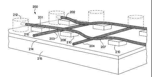
FIG. 8 shows an example of a crossbar array of the present invention. In FIG.
8,
crossbar array 200 comprises wires 201-204 supported, by various means, on a
substrate
comprising a thin dielectric layer 214 (e.g., Si02) which terminates
conducting layer 215
(e.g., highly doped silicon). Wire 203 is parallel to wire 204 and these are
crossed with
parallel wires 201 and 202. FIG. 8 shows wires 201 and 202 perpendicular to
wires 203 and
204, and typically this arrangement provides high symmetry, allowing facile
integration with
other systems. Of course, wires do not have to be crossed at 90 angles and
can be crossed at
any angle as desired.
At least two crossed wires can define a junction, e.g., wire 201 is disposed
adjacent
wire 203 at junction 206. "Disposed adjacent" does not require that wires 201
and 203 be in
contact with each other, but rather that wires 201 and 203 are positioned
relative to each other
such that they are capable of contacting each other. The wires can be free of
contact with no
other material intermediate the wires, or spacing between the wires can be
provided with the
aid of intermediary material (for example, see FIGs. 5 and 6 and accompanying
discussion).
The ability of the crossed wires to contact and release from each other
reversibly at cross
point junctions provides the basis for addressable elements, such as switches,
memory
elements and diode junctions.
In one embodiment, wires 203 and 201 are disposed adjacent each other by
positioning wire 203 directly on substrate 214. Wire 203 (and 204) is referred
herein as an
example of a "bound" wire. Wire 203 is intermediate substrate 214 and wire
201. Wire 201
is supported above wire 203, relative to substrate 214, by supports 210. Wire
201 (and 202)
is referred herein as an example of a "supported" wire. Supports 210 can be
spaced
periodically on either side of each bound wire (e.g., wires 203 and 204). This
arrangement of
supports 210 allows each junction (e.g., junctions 206 and 207) to be
addressed
independently of each other.
In another embodiment, wires 201 and 203 can be disposed adjacent each other
by
positioning wire 203 in a trench. Referring to FIG. 10B, device 230 features
parallel trenches
CA 02372707 2001-11-01
WO 01/03208 PCT/US00/18138
-10-
232. Bound wires are nested in each of trenches 232 which are of sufficient
depth to prevent
the bound wires from projecting above substrate surface 235. A parallel array
of crossed
wires 233 can be positioned across trenches 232. Again, bound and support
wires should
have sufficient spacing from each other to allow contact with each other and
release from
each other at junctions.
Referring back to FIG. 8, at least one end of each of wires 201-204 is in
electrical
contact with one of contact electrodes 212. That is, in one embodiment, at
least one wire is
attached to the contact electrode. The attachment can be provided by
covalently attaching at
least one wire to the contact electrode. The electrode can comprise any
material capable of
electrical conduction, as is known in the art.
FIG. 8 shows wires 201 and 203 not in contact, i.e., free of contact, with
each other.
"Free of contact" refers to a sufficient gap between crossed wires such that
there is no
conduction pathway between wires 201 and 203. Supported wires such as wire 201
preferably are selected to possess a stiffness to allow periodic support
above, yet free of
contact with, wire 203.
In contrast, wires 201 and 204 are in contact with each other at junction 207.
"Contact" can refer to electrical contact, in which there is a conduction
pathway between
wires 201 and 204, or in van der Waals contact with each other. Often, for
conducting wires,
van der Waals contact provides electrical contact. To achieve such contact,
wire 201 is
capable of deformation localized at a region around junction 207. Thus, the
wire of the
present invention should have a sufficient Young's modulus such that the wire
is capable of
deformable van der Waals contact with the crossed wire at junction 207. In
addition, this
deformation occurs without affecting neighboring junctions, i.e., wires at
neighboring
junctions can independently undergo deformation or remain free of contact with
a crossed
wire.
It is another feature of the array of the present invention that deformation
occurs via
application of a stimulus. Typically, the stimulus is an electrical stimulus
as provided
through the at least one electrode 212. A stimulus can comprise biasing the
two crossed
wires with opposite polarities such that electrical attraction causes wire 201
to deform
towards wire 207. In addition, wires 201 and 204 preferably are selected to
have sufficient
adhesion energy to maintain deformable van der Waals contact upon removal of
the stimulus.
Thus, no applied energy is required in preferred embodiments to maintain wires
201 and 204
CA 02372707 2001-11-01
WO 01/03208
PCT/US00/18138
-11 -
in contact with each other. The benefits of this capability are discussed
below with respect to
the potential for the crossbar array of the present invention to provide
bistable (i.e. non-
volatile) elements.
It can be seen that bound wires 203 and 204 do not require deformation of any
type.
Supported wires 201 and 202, however, should have sufficient stiffness to
remain supported
above bound wires, yet have sufficient flexibility to enable deformation to
contact the bound
wires without breaking and have sufficient adhesion energy to maintain van der
Waals
contact. Furthermore, supported wires 201 and 202 should be of sufficient
robustness to
withstand the strain of several deformation processes. Carbon nanotubes
possess all these
properties and are a preferred material for supported wires of the crossbar
array. Of course,
carbon nanotubes can be used as the bound wires. In addition, the supported
wires should
have enough friction to prevent slippage on supports, particularly during
deformation
processes. The interaction with the support could be further enhanced through
chemical
modification, if required, although this is not always necessary.
A device that is capable of maintaining at least two different states, e.g.,
contact
between crossed wires or lack of contact between crossed wires without the
need for applied
energy to maintain either state, is referred to as a "bistable" device. As an
example, bistable
device elements provided by the invention at junctions of crossbar arrays will
now be
described. Bistable elements of the invention include those in which each of
the two states is
stable or metastable. These bistable elements have, as a common feature,
nanoscopic scale
electromechanical switching between "on" and "off' states where the "on" state
involves
nanoscopic-scale wires in electrical contact at the crossbar junction and in
the "off' state the
nanoscopic-scale wires are free of electrical contact (separated). Reading the
"on" or "off'
state of any cross junction is easily accomplished by measuring the
resistance/conductance of
the junction. The two states in this device architecture can be easily
distinguished
independent of fluctuations in the "on" state resistance. The "off' state
conductance is lower
than a conductance of the "on" state to an extent limited only by detection
sensitivity, for
typical bistable structure parameters. For example, for carbon nanotubes
calculations suggest
a change in "on" to "off' state resistance by a factor of 103 to 106 for
typical device
parameters (i.e. for typical nanotube separations in the "off' state). The
device architecture
and function is thus highly robust.
CA 02372707 2001-11-01
WO 01/03208 PCT/US00/18138
- 12 -
The operation of bistable switching elements of the invention now will be
described
with reference to FIG. 2. FIG. 2 shows arrangement 26 and 28, each including a
crossbar
array junction 32. With reference to arrangement 28 of FIG. 2, the "off" state
is at
mechanical equilibrium, i.e. when the crossed nanotubes are separated as
illustrated. As a
voltage is established between wires 18 and 30 that attracts them to each
other, wire 30 is
deflected towards wire 18 and contacts wire 18, defining the "on" state,
corresponding to van
der Waals contact. The conduction between the crossing nanoscopic wires is
either high or
low in the "on" and "off" states, respectively. In the "on" state, the
conduction is defined by
the approximate constant wire/wire contact at the cross. In the "off' state,
conduction occurs
by quantum mechanical tunneling and will be much lower. The bistable device
includes
stable minima at both the "off' and "on" states by virtue of mechanical
equilibrium and van
der Waals contact, respectively, and can be switched "on" by biasing the
nanotubes with
opposite polarity. The electrostatic term lowers the potential minimum at
contact and
ultimately eliminates the barrier between "off' and "on" states to enable
switching. Removal
of the potential leaves the system in a stable "on" state. The device can be
switched to the
"off' state in a similar manner by applying the same potential to both tubes.
Switching
between the "on" and "off' states at reasonable (approximately 4-5 Volts)
potentials is
facilitated. A second general class of electromechanical switches (e.g.
arrangement 26 of
FIG. 2) are based on crossbar SWNT arrays that are initially in a contact "on"
state at rest,
but when electrostatically separated enter a second potential "off' minimum.
Nanoscopic-scale devices of the invention can exhibit switching times on the
order of
6-30 picoseconds, thus they can operate at a frequency of as high as about 200
GHz. Thus,
the invention encompasses low frequency devices also. Moreover, the energy to
switch an
individual device is extremely small. Much lower power is required than for
silicon DRAMs
at similar frequencies. Additionally, nanotubes have extremely good thermal
conductivity
along their tube axes and thus are an ideal structure for removing heat from a
highly
integrated device.
In addition, the nanoscopic-scale device of the present invention displays
stability at a
wide range of temperatures, limited only by the stability of the metal
contacts. For example,
memory elements provided from carbon nanotubes exhibit an intrinsic thermal
stability up to
or higher than 1000 C. The memory elements also exhibit radiation stability
and non-
volatility of the stored information.
CA 02372707 2001-11-01
WO 01/03208 PCT/US00/18138
- 13 -
FIG. 4 illustrates, schematically, energy curves associated with "on" and
"off' states
of a memory element 32 of a device according to one embodiment of the
invention in which a
first electronic conductor is suspended above and free of contact with a
second electrical
conductor in its lowest energy configuration (e.g. arrangement 28 of FIG. 2).
Curve 51
represents the energy states in the various conformations. The lowest energy
configuration at
mechanical equilibrium is the "off' state where the crossed conductors are
separated. The
"on" state corresponds to a Van der Waals contact. Conduction between the
crossed wires is
high in the "on" state and low in the "off' state. Switching is carried out as
follows.
Switching from the "off' state to the "on" state (following the energy plot of
curve 56) is
carried out by biasing the wires 18 and 30 with opposite polarity so that they
are attracted
toward each other until reaching a stable Van der Waals contact distance
(Zvd,,). Switching
"off', following the energy plot of curve 54, is accomplished by biasing wires
18 and 30 with
the same polarity so that they repel each other, moving toward their
mechanical equilibrium
distance (Zo). The device of the invention is highly efficient in that
switching between "off'
and "on" states can be carried out at approximately 4-5 volts, and no external
power is
required to maintain the wires in either the "on" or "off' states (i.e.
bistable, non-volatile).
The "off' and "on" states can be read easily by measuring a resistance of the
junctions. In one embodiment, a difference between the resistance between two
crossed
wires must be sufficient to differentiate between the "on" and "off' position.
One aspect of the invention involves the spatially-controlled formation of
nanoscopic-
scale wires into well-defined crossbar arrays. Two general techniques for
spatially-controlled
formation are described herein, one involving directed assembly of pre-formed
nanoscopic-
scale wires onto a surface in a desired pattern, and the second involving
growth of
nanoscopic-scale wires on a surface in a desired pattern directed, for
example, by electric
fields, highly-directional precursor flow rates ("precursor wind"), template-
directed growth
(growth within host channels; mechanically-directed growth), growth and
assembly within
host materials such as self-assembled block copolymers, inorganic host
structures, and the
like. Relatively simple (1 x 1) crossbar arrays are provided in addition to
more highly
integrated arrays, for example, 1 x 8, 8 x 8, 16 x 16 arrays, etc. The arrays
can serve as
memory devices, where junctions of the arrays can function as memory elements.
Alternatively, the junctions can serve as diodes, for overcoming problems such
as cross-talk,
as described below.
CA 02372707 2009-05-22
64371-434
- 14 -
Referring now to FIG. 1, a technique for directed assembly of a pre-formed
nanoscopic wire onto a chemically patterned surface is illustrated
schematically. In FIG. 1 a
silicon/silicon dioxide substrate 10 is provided and coated with a self-
assembled monolayer
(SAM) 12 of alkylsilane, uniformly. In one example of patterning the SAM for
directed
assembly of nanoscopic scale circuitry atomic force microscopy (AFM) then is
used to write,
at high resolution, a pattern in SAM 12 at which the SAM is removed. The
pattern can be for
example linear, or a crossed array of lines linear in embodiments for making
nanoscopic
crossed arrays. As illustrated, the pattern is linear and results in a linear
patterned SAM 14
on substrate 10 defining lines of alkylsilane separated by a linear region
free of SAM. In
another technique, microcontact printing can be used to apply patterned SAM 14
to substrate
10. Microcontact printing is described below.
Next, open areas in the patterned surface (the SAM-free linear region between
linear
SAM 14) is filled with an amino-terminated SAM that interacts in a highly
specific manner
with a nanoscopic wire such as a nanotube. The result is a patterned SAM, on
substrate 10,
including linear SAM portions 14 of methyl terminated material (methyl groups
exposed at
the surface) separated by a line 16 of amino-terminated SAM material. Of
course, any
desired pattern can be formed where regions of the amino-terminated SAM
material
corresponds to regions at which wire deposition is desired. The patterned
surface then is
dipped into a suspension of wires, e.g. nanotubes, and rinsed to create an
array in which wires
18 are located at regions 16 of the SAM. Where nanotubes are used, an organic
solvent such
as dimethyl formamide can be used to create the suspension of nanotubes.
Suspension and
deposition of other nanoscopic-scale wires is achievable with easily selected
solvents.
Any of a variety of substrates and SAM-forming material can be used along with
microcontact printing techniques, such as those described in international
patent publication
WO 96/29629 of 'Whitesides, et al., published June 26, 1996.
Patterned SAM surfaces can be used to direct a variety of nanoscopic wires or
nanoscopic-scale electronic elements. SAM-forming material can be selected,
with suitable
exposed chemical functionality, to direct assembly of a variety of electronic
elements.
Electronic elements, including nanotubes, can be chemically tailored to be
attracted
specifically to specific, predetermined areas of a patterned SAM surface.
Nanotubes are
particularly suitable for chemical functionalization on their exterior
surfaces, as is well
known.
CA 02372707 2009-05-22
= =
64371-434
- 15 -
Chemically patterned surfaces other than SAM-derivatized surfaces can be used,
and
many techniques for chemically patterning surfaces are known. Suitable
exemplary
chemistries and techniques for chemically patterning surfaces are described
in, among other
places, international patent publication serial no. WO 97/34025 of Hidber, et
al, entitled,
"Microcontact Printing of Catalytic Colloids", and U.S. patent nos. 3,873,359;
3,873,360; and
- 3,900,614, each by Lando. Another
example of a chemically patterned surface is a micro-phase separated block
copolymer
structure. These structures provide a stack of dense lamellar phases. A cut
through these
phases reveals a series of "lanes" wherein each lane represents a single
layer. The block
copolymer is typically an alternating block and can provide varying domains by
which to
dictate growth and assembly of a nanoscopic wire.
While FIG. 1 illustrates, schematically, assembly of a nanoscopic wire on a
SAM in a
pattern dictated by the SAM, and a SAM defining a delineated pattern with a
nanoscopic wire
associated with the self-assembled monolayer, FIG. 2 illustrates,
schematically, creation of a
crossed microscopic wire array using self-assembled monolayer pattern
direction. In FIG. 2 a
substrate 10 including a SAM pattern having portions 14 and 16, as described
with reference
to FIG. 1, and a microscopic wire 18 formed on portion 16 of the SAM is
illustrated. AFM or
another technique (e.g., electron-beam lithography, etc.) can be used to write
a linear pattern
orthogonal to the original wire orientation in regions 20 of sections 14 of
the SAM. Next, the
open areas in the patterned surface are filled with amino-terminated SAM of
the same length
(amino-terminated SAM sections 22) or greater length (SAM sections 24)
compared to the
original SAM pattern. This results in an arrangement 26 in which all SAM
material is of the
same height, or an arrangement 28 in which portions of the SAM arrangement
extend above
the plane of the original SAM and, optionally, above the height of the wirel8
to provide
clearance above the wire. The patterned surface then is dipped into a
suspension of
additional nanoscopic-scale wires and rinsed to create a crossbar array. In
arrangement 26 a
wire 30 is arranged in crossbar array formation across original wire 18 at
junction 32, in
contact with wire 18. Arrangement 28 defines an electrical crossbar array
comprising at least
two nanoscopic wires in crossbar array orientation, where the crossbar array
is made up of
wires that are not in contact with each other at the junction. These
arrangements can be used
directly as a bistable device memory element, as will be apparent to those of
ordinary skill in
the art with the benefit of the description below.
CA 02372707 2001-11-01
WO 01/03208 PCT/US00/18138
- 16 -
Described above are techniques for assembly of pre-formed nanoscopic-scale
electronic elements onto a surface. Another general technique included in the
invention for
creation of nanoscopic-scale electronic devices involves directed growth of
nanoscopic-scale
elements on a surface in a predetermined pattern. FIGs. 3A and 3B illustrate,
schematically,
one such technique involving formation of crossbar arrays via CVD in the
presence of
electric fields. In FIG. 3A, an array of catalytic sites 34 are arranged
opposite each other and
define desired end points of parallel nanoscopic wires of a crossbar array
(although pairs of
catalytic sites are illustrated, as described below only one catalytic site
per wire is needed).
Clusters 34 are used to direct the growth of bridging nanoscopic-scale wires
in a direction in
the presence of an electric field. An electric field is oriented in a
direction parallel to (in the
direction of) the desired direction of wire growth using electrodes 36 and 38,
connected by an
electrical circuit 40, oriented behind each array of the diametrically opposed
catalytic sites.
The underlying basis for the technique is that the energy of a polarizable,
anisotropic
structure such as a nanoscopic-scale wire formed in accordance with the
invention is lower
when its long axis is aligned with the field. Correspondingly, when an
anisotropic structure
is misaligned, there is a force exerted on the structure to bring it into
alignment. This basic
concept of electric field alignment has been used previously for the alignment
of anisotropic
molecules through micron scale fibers, and thus the technique will be
understood by and
reproducible by those of ordinary skill in the art with the benefit of the
instant disclosure.
The highly anisotropic, or one-dimensional, structure of nanotubes, especially
SWNTs, leads
to a much greater polarization anisotropy (exceeds 1,000:1 along the tube
axis) than would be
present for a three-dimensional material of similar dimensions (for example, a
copper
nanowire), thus nanotubes are particularly preferred for this technique. This
will lead to
greater energy/force terms for the nanotube aligned with the field. Any slight
misalignment
with the field during nanotube growth is corrected as the force acting to re-
orient it with the
field becomes increasingly large as the nanotube grows. An alternative
mechanism, for
aligning nanotubes growing from an electrode is the accumulation of a net
charge on a
nanotube and electrostatic attraction to an oppositely biased electrode.
According to the
technique, the array of diametrically opposed catalytic sites 34, in the
presence of an electric
field produced by circuit 40 and electrodes 36 and 38, is exposed to
conditions of chemical
vapor deposition allowing growth of a nanotubes 42 between the catalytic
sites.
CA 02372707 2001-11-01
WO 01/03208 PCT/US00/18138
- 17 -
Re-orientation of the structure such that a series of catalytic sites 44 are
diametrically
opposed in a direction perpendicular to catalytic sites 34, with creation of
an electrical field in
a direction perpendicular to nanotubes 42, and exposure to chemical vapor
deposition
conditions results in deposition of nanotubes 46 aligned in crossbar array
orientation
perpendicular to nanotubes 42.
Catalyst sites for growing nanoscopic wires can be patterned by lithographic
techniques, self-assembly with or without host phases, or patterning via
proximal probes (e.g.
dip pen lithography).
As mentioned, only one catalyst site per wire is required. With reference to
FIG. 3A,
one set of catalytic sites 34 can be provided and, in the presence of an
electric field and
exposure to conditions of CVD nanotubes can be grown from each catalytic site
extending
away from each site in the same direction to form an array of nanotubes 42 as
illustrated.
Similarly, with reference to FIG. 3B, only one set of catalytic sites 44 is
required. As
mentioned above also, other techniques for directing growth of nanoscopic-
scale wires can be
used such as highly-directional precursor flow rates, template-directed
growth, growth within
host materials, etc.
A combination of techniques to form crossbar arrays of the invention can be
used.
With reference to FIG. 2, wires 18 can be formed by any technique, including
conventional
lithographic techniques. Then, directed growth of nanoscopic-scale elements
can take place
across SAM sections 22 or 24 resulting in arrangements 26 and 28,
respectively.
Nanoscopic wires can also be formed on a surface in a pattern dictated by a
mechanically patterned surface. Mechanically patterned surfaces can be
provided by walls,
channels, trenches, capillaries or the like. Referring back to FIG. 10,
article 220 features a
plurality of parallel trenches 222 which can be provided in a substrate
surface by a variety of
means, including lithographic techniques, microcontact printing, nano-
imprinting, nano-
machining, etching, whether by chemical etching, laser etching, or by a
focused ion beam
(FIB) machine, and related techniques. Alternatively, some substrates, such as
vicinal
surfaces or lattice mis-matched hetero-epitaxial structures inherently exhibit
such trenches,
and thus can also be used as article 220. Article 220 features trenches 222
milled by an FIB.
The trenches can serve as a mechanical guide for the growth of nanowires, such
as by CVD
growth techniques. Crossed wires 233 (FIG. 10B) can be grown by providing a
plurality of
catalyst nanoparticles 224 (i.e., catalytic sites, FIG. 10A) linearly disposed
parallel to
CA 02372707 2001-11-01
WO 01/03208 PCT/US00/18138
- 18 -
trenches 222 and along an edge of article 220. FIG. 10B shows how growth of
nanowires
233 can be directed from sites 234 over trenches 232 by techniques such as
CVD. The
growth can be directed under a local electric field parallel to the surface.
The origin of
growth is defined by the patterning the catalyst nanoparticles.
Another example of wire growth along a substrate involves an article having a
plurality of indentations and protrusions. By positioning protrusions on the
substrate
surfaces, cavities are formed and defined by the substrate surface and the
plurality of
indentations. These indentations can have the shape of capillaries. The
capillary walls can
be used to mechanically direct growth originating from a catalytic site or can
be used to
chemically pattern a surface which in turn directs growth of the nanowire.
Nanoscopic wires can also be formed on a surface in a pattern dictated by gas
flow.
For example, disposing a series of catalyst nanoparticles (i.e., catalyst
sites) and subjecting
these nanoparticles to a gas flow of high pressure can direct growth of a
nanowire in the
direction of gas flow. Particularly, this method provides a novel growth
technique where the
gas comprises a reactant for the nanowire. For example, carbon precursor gases
such as
ethylene, acetylene, methane or carbon monoxide can be used to grow carbon
nanotubes
whereas silane can be used to grow silicon nanowires. Other precursors are
also well known
in the art.
Referring again to FIG. 3A and 3B, through placement of catalytic sites 34 and
44
adjacent a series of contact electrodes (not shown), or use of the catalytic
sites 34 or 44 as
contact electrodes where they are electrically conductive and provide good
electric contact
with nanotubes, each of the nanotubes can be provided in electrical contact
with a different
contact electrode. Covalent attachment between nanotubes and contact
electrodes is
preferred, and is easily facilitated by functionalizing the nanotubes, at
their ends, with a
molecule that can attach, preferably covalently, to a contact electrode.
Functionalization of
nanotubes is known, and functional groups that attach to materials that can
serve as contact
electrodes are known, thus the technique of the invention is readily
facilitated based on the
instant disclosure. In one embodiment, the ends of the nanotubes are
functionalized with
conjugated thiols, and the contact electrodes are gold. See, for example,
Wong, et al.,
"Covalently Functionalized Nanotubes as Nanometer Probes for Chemistry and
Biology"
Nature 394, 52-55 (1998); Wong, et al., "Covalently-Functionalized Single-
Walled Carbon
Nanotube Probe Tips for Chemical Force Microscopy" .1 Am. Chem. Soc. 120, 8557-
8558
CA 02372707 2009-05-22
=
64371-434
- 19 -
(1998). The end states of the nanotubes can effectively
couple to bulk conduction channels in the nanotubes as described by Kim, et
al., "Electronic
Density of States of Atomically-Resolved Single-Walled Carbon Nanotubes: Van
Hove
Singularities and End States" Phys. Rev. Lett. 82, 1225-1228 (1999) .
Using the techniques of the invention it is possible to achieve an active
element two-
dimensional density of as high as about 1012 memory elements/cm2. Thus, low or
high
density arrays are envisioned. These element can be used to construct non-
volatile random
access memory (RAM), read-only memory bits and configurable logic, among other
applications. This is facilitated where an array of nanoscopic wires 42 (FIG.
3B) are
positioned at 20-nanometer intervals. Where wires 46 are similarly arranged,
this density is
achieved. By using nanoscopic wires such as nanotubes of 10 micron length,
with a memory
element every 20 nanometers along each nanotube, an array can be formed with
at least 500
parallel wires in each direction, each wire containing at least 500 crossbar
array junctions
(memory elements). At least 250,000 memory elements can be formed in such an
array.
Three-dimensional arrays can be created as well, and can have higher
integration densities
than two-dimensional arrays. Three-dimensional arrays are produced using multi
layer
architecture extended from that described above with reference -to FIG. 2 or
from assembly
using block polymers as directing agents.
As mentioned above, the invention provides a series of memory elements in a
crossbar array that can be written and read (switched between "on" and "off'
settings)
without auxiliary circuitry addressing each element. For example, FIG. 5 shows
element 32
is a bistable element in that it is stable in both the "on" and "off' states,
and free of auxiliary
elements, such as capacitors, transistors and switches.
Referring now to FIG. 5, a stable/metastable memory element 32 according to
arrangement 26 of FIG. 2 is illustrated, schematically and graphically. As
illustrated, two
touching crossed wires 18 and 30 in the "on" state are biased against an
underlying ground.
Curve 70 represents the energy states in the various conformations. Switching
"off' (curve
74): when the wires are biased with similar polarity, they are repelled from
each other and
spatially separated. They can rapidly return to a metastable distance where
they are separated
by space or molecules 72 filling the gap between them. This metastable "off'
state slowly
relaxes back to the "on" state within a retention time. Switching "on" (curve
76): when the
CA 02372707 2001-11-01
WO 01/03208 PCT/US00/18138
- 20 -
nanotubes are biased with opposite polarity, they attract each other,
accelerate their relaxation
to a van der Waals contact distance. FIGs. 6A - 6C illustrate various
embodiments in which
oppositely charged molecules are allowed to organize within cross junctions
between
nanotubes in the "off' state according to the arrangement of FIG. 5. These
molecules can
include short charged polymers 60 (FIG. 6A), surfactant molecules 62 that can
form micellar
structures around nanotubes (FIG. 6B), polymer brushes 64 grafted to a SAM
that forms a
basis of the structure (FIG. 6C), and the like.
Another aspect of the invention provides an article comprising an electrical
crossbar
array comprising at least two crossed wires defining a diode. The device is
free of auxiliary
circuitry other than the at least two crossed wires defining the diode. For
example, if bound
wires are semiconducting and support wires are metallic conductors, contact
between the two
wires will provide a metal/semiconductor junction, which functions as a
rectifying Schottky
diode at the contact junction. Thus, an on junction provides intrinsic
rectifying behavior.
Currently, nanotubes exist as a mixture of semiconductor and metallic
conductor nanotubes.
It has not been possible to separate the mixture into purely semiconducing
nanotubes and
metallic nanotubes. Rectifying junctions can also be provided by providing
semiconductor
nanowires, preferably n-type. For metallic nanotubes, a rectifying Schottky
junction will
result in the "on" state while for semiconducting nanotubes (which are
intrinsically p-type) a
rectifying p/n diode junction will result if the semiconducting nanowire is n-
type doped.
The provision of diode junctions can eliminate the problem of cross talk in
crossbar
arrays. FIG. 9A shows an example of a 2 x 2 array in which bit [21] is off.
Thus, a direct
conducting path between bit [21] and bit [11] is not acceptable. Because there
is no
restriction on a direction for a conduction pathway, a pathway as represented
by bold line 250
can circumvent the [21]/[11] pathway. This will cause bit [21] to appear on
even though it is
off. FIG. 9B shows a result of rectifying behavior when one set of crossed
wires comprises a
semiconductor and the other set of crossed wires comprises a metallic
conductor. Conducting
is limited to one direction only and cross talk is thus prevented.
As mentioned previously, providing pure semiconductor nanotubes or metallic
nanotubes has not been possible to this point. Thus, another aspect of the
present invention
provides a method involving a mixture of metallic nanotubes and semiconducting
nanotubes.
The method involves separating the metallic nanotubes from the semiconducting
nanotubes.
It is known that metallic nanotubes have a greater polarizability than
semiconducting
CA 02372707 2001-11-01
WO 01/03208 PCT/US00/18138
- 21 -
nanotubes by about three orders of magnitude. Thus, in one embodiment, the
step of
separating the mixture involves subjecting the mixture to an electric field of
intensity
sufficient to selectively orient metallic nanotubes. Depending on the
intensity of electric
field, there is a critical length below which only metallic nanotubes will be
aligned. Thus, the
intensity can be adjusted to be in accord with a field below the critical
length. Above this
critical length, both types of nanotubes can be aligned by the field. Below
this length, the
electric field is of an intensity such that the semiconducting nanotubes
remain unoriented
with respect to the electric field. Once selective alignment is achieved,
separation is routine.
As noted above, it is a significant advantage of the invention that junction
elements
can be switched between "on" and "off' states remotely, i.e., by simply
addressing at least
one end of each of the wires that cross to form the memory element (wires 18
and 30 in FIGs.
2 and 4). Where the junction elements comprises memory elements, or diodes,
some or
preferably all of the memory elements are free of auxiliary circuitry defining
the memory or
diode elements and free of auxiliary circuitry addressing the memory or diode
elements to
switch them between states; the memory or diode element simply includes wires
18 and 30
that define the lead wires addressing the memory or diode element. Those of
ordinary skill in
the art will understand the meaning of auxiliary circuitry for switching a
memory or diode
element between "on" and "off' states, auxiliary circuitry defining memory
states
themselves, and the meaning of a device free of these components. An example
of auxiliary
circuitry defining memory states themselves includes an electrical pathway
connecting two
crossed conductors at a junction that can be switched from a conducting state
to a non-
conducting state. An example of auxiliary circuitry for switching a memory
element between
states includes circuitry connected to the electrical pathway that can be
switched to render the
pathway conducting or non-conducting.
One feature of the invention is that, with reference to FIG. 2, nanoscopic -
scale wires
18 and 30 need not each be flexible nanoscopic wires such as nanotubes. As can
be seen
from the illustration and description relating to FIGs. 4 and 5, memory
elements of the
invention each include one wire (wire 18 in FIGs. 4 and 5) that need not move
during
switching, and can be made of essentially any material having appropriate
conductivity that
can be formed in the appropriate dimensions. Although nanotubes and other
nanoscopic
wires can be used for fixed wires 18, wires formed by more conventional
techniques such as
lithography can be used as well. Wire 30 should be selected to meet the
additional
CA 02372707 2001-11-01
WO 01/03208 PCT/US00/18138
- 22 -
requirement of repeated flexure during switching between "off' and "on"
states, as
illustrated. Wire 30 should thus be selected to have elasticity and robustness
to meet this
demand. Nanotubes exhibit such robustness and are ideal for use as flexing
wires 30 in the
invention. Thus, devices of the invention can be constructed entirely by
directed assembly of
pre-formed wires onto a surface or entirely from directed growth of wires at a
surface, or a
combination, or fixed wires 18 can first be formed via a conventional
technique such as
lithography followed by placement of flexing wires 30 by directed assembly, or
directed
growth.
Referring now to FIG. 7, a cut away schematic illustration of a crossbar array
80 of
the invention is presented. Array 80 includes a series of parallel, equally-
spaced wires 82,
84, 86, 88..., and a series of parallel, equally-spaced wires 100, 102, 104,
106... that cross (are
perpendicular to) wires 82, 84.... Each of wires 82, 84, 86... is addressed by
an electrode 120,
122, 124... at one end thereof and each of wires 100, 102, 104, 106... is
addressed by an
electrode 140, 142, 144... at one end thereof It is a feature of the invention
that wires 82, 84,
86... and wires 100, 102, 104... require electrical contact with only one
electrode, i.e., one
interconnect can be used to address many individual junctions. Electrodes can
be provided at
opposite ends of the wires from those ends at which electrodes are shown
(opposite ends not
shown in FIG. 7), but this is optional. Each of wires 82, 84, 86... crosses
each of wires 100,
102, 104..., each crossed wire junction defining a memory element as
illustrated in FIGs. 2, 4,
and 5 and discussed above. For example, junction 160 is a memory element
defining the
intersection of wires 88 and 104. When device 80 is constructed of memory
elements as
illustrated in arrangement 28 of FIG. 2, and in FIG. 4, at mechanical
equilibrium wires 88 and
104 are free of contact and element 160 is "off'. Biasing electrodes 126 and
144 at opposite
polarity brings wires 88 and 104, at junction 160, into contact with each
other (stable Van der
Waals contact) and junction 160 is switched "on". Bias need not be maintained
between
electrodes 126 and 144 to maintain element 160 in the "on" state in preferred
embodiments.
To switch element 160 "off', electrodes 126 and 144 are biased with the same
polarity to
repel wires 88 and 104 from each other at junction 160. Where device 80
includes junctions
as illustrated in arrangement 26 of FIG. 2 and FIG. 5, at mechanical
equilibrium junction 160
is in the "on" state with wires 88 and 104 contacting each other, and element
160 is switched
"off' by biasing electrodes 126 and 144 at similar polarity. Switching element
160 back "on"
is accomplished by biasing electrodes 126 and 144 at opposite polarity.
CA 02372707 2001-11-01
WO 01/03208 PCT/US00/18138
- 23 -
Another aspect of the present invention provides an article comprising an
electrical
crossbar array comprising at least two crossed nanoscopic wires defining a
memory element
capable of being switched irreversibly between at least two readable states.
Thus, the device
is "read-only". In another embodiment, the article comprises an electrical
crossbar array
comprising at least two crossed nanoscopic wires defining a memory element
capable of
being switched reversibly. Thus, the devices can be used for a volatile RAM
(e.g. require a
power supply to keep the stored information) or a non-volatile RAM.
Example 1
To quantify the bistability and switching behavior of the device element a
total
energy, ET, can be calculated:
ET= Evdw Eeias + Eelec
(1)
where Ed w is the van der Waals (vdW) energy, Eelas is the elastic energy and
Eeiec is the
electrostatic energy for the device. The first two terms in (1), which define
the static
potential, can be evaluated to assess the range of parameters that yield
bistable devices. FIG.
11 shows plots of energy, ET = Evc1W Eelas , for a single 20 nm device as a
function of
separation at the junction. The series of curves correspond to initial
separations of 0.8, 1.0,
1.2, 1.4, 1.6, 1.8, 2.0, 2.2, 2.4 nm for carbon nanotubes, with two well-
defined minima
observed for initial separations of 1.0 to 2.0 nm. These minima correspond to
the crossing
nanotubes being separated (2.4 nm) and in vdW contact (0.8 nm). The vdW
interaction
between nanotubes can be calculated by pairwise summation of a Lennard-Jones
potential
that has been shown previously to provide good agreement with experiment for
fullerene and
nanotube systems. The elastic contribution to the total energy can be
determined using a
beam mechanics model:
6(k 3B)1/4
E elas = (&)2
(2)
A/2[3+ 3 i6L + 3(6L)2 + (fiL)3
where B is the product of the nanotube elastic modulus and geometric moment of
inertia, k is
the elastic modulus of the support, L is the length of the suspended nanotube,
,IA
fi = A/ ( D
i)" ", and az is the displacement of the suspended tube from its unstrained
2
CA 02372707 2001-11-01
WO 01/03208 PCT/US00/18138
- 24 -
position. These calculations show that the proposed SWNT device structure
exhibits
bistablility for a broad range of parameters (FIG. 11). For example, a 20 nm
device in FIG.
11 exhibits room temperature stable (i.e., barrier >>10kBT) on and off states
for initial
separations ranging from 1.0 to 2.2 nm. The calculated structures of the SWNT
device
element in the off state and on state for an initial separation of 2 nm (FIG.
12) highlight the
relatively minor distortion of the upper SWNT in the on state, even when the
initial
separation is near the upper limit for bistability. Si support structures
(elastic modulus of 16
GPa) are not shown for clarity. These calculations also show that the
potential is bistable for
a wide range of device sizes when the upper nanotube is supported on either
hard materials,
such as silicon (FIG. 13) or soft organic (FIG. 14) materials. FIG. 14 shows
calculations on
an organic layer having an elastic modulus of 12 GPa. In FIGs. 13 and 14, the
range of initial
separations yielding bistable devices is shown in gray. Importantly, soft
supports enable
bistability for smaller devices. Both types of materials can be used for
device fabrication. In
general, the bistable region increases with device size, and the softer
organic support yields a
larger range of bistability especially in the smallest structures. The
calculations were 15
carried out for (10,10) SWNTs with an elastic modulus of 1 TPa, and Lennard-
Jones
parameters of C6 = 32.00 x 10-60 erg cm6 and C12 = 55.77 x 10-105 erg cm12.
There are several important points that can be drawn from these calculations.
Foremost, is the wide range of parameters that yield a bistable potential for
the device
configuration. The robustness of the on/off states suggests strongly that this
architecture will
be tolerant of variations in structure that inevitably arise during
fabrication by, for example,
self assembly. Second, the differences in separation between nanotubes in the
on and off
states will produce large differences in resistance (i.e., I ¨ exp(-kd), where
I is the current, k
is a decay constant of order 2 kl and d is the tube-tube separation in
angstroms), and thus
should enable reliable reading of the on/off states independent of variations
in cross contact
resistance. Third, the range of mechanical strains required to achieve
bistability in FIG. 11,
0.22 ¨ 1.7 %, is well below the elastic limit of at least 6% determined
computationally and
experimentally for SWNTs, and the average bending angle in the on state is ca.
1/2 that
required to buckle nanotubes. Hence, these device elements can be robust as
required for a
reliable molecular scale computer. Comparison of the calculated strain
energies to values of
the nanotube-surface interaction and friction suggests that (i) the lower
nanotube remains
fixed on the substrate, and (ii) the suspended nanotubes do not lift off or
slip on supports on
CA 02372707 2001-11-01
WO 01/03208 PCT/US00/18138
- 25 -
the order of 10 nm when the suspended tube is deflected to the on state. The
interaction with
the support could also be enhanced through chemical modification.
Example 2
The effectiveness of switching the suspended nanotube devices between on and
off
states has been assessed by evaluating the voltage-dependent contribution of
the electrostatic
energy to the total energy. In this calculation, the boundary element method
was used to
numerically solve the Laplace equation for the complex three-dimensional
geometry of the
crossed nanotube device. Calculations of ET for switching a 20 nm device on
and off (FIG.
15) demonstrate that it is possible to change reversibly between the on/off
states using
moderate voltages, which do not exceed the threshold field for nanotube
failure. The
switching voltages vary depending on the specific device geometry (i.e., shape
of the static
potential), and thus can be further optimized. For example, by using a thinner
dielectric layer
(that is, 4 vs 20 nm Si02) the on and off switching thresholds can be reduced
from 4.5 and 20
V to 3 and 5 V, respectively. The calculations also show that the
electrostatic forces between
adjacent nanotubes are insufficient to distort an array of elements, even at a
10 nm device
scale, because most of the electrostatic interaction is localized in the small
crossing region of
the individual elements.
This example provides a demonstration of electrostatic switching of the
nanotube
device. FIG. 15 shows plots of the energy, ET = EvdW + Eelas + Eekctro , as a
function of
separation at the junction for switching on (FIG. 15A) and switching off (FIG.
15B). In FIG.
15A, the plots (i), (ii) and (iii) correspond to ET for V1-= V2 = 0 V, V1 =
+3; V2 = -3 V and V1
= +4.5; V2 = -4.5 V, respectively, where Vi and V2 are the potentials applied
to the two
crossing nanotubes. In FIG. 15B, (i), (ii) and (iii) correspond to V1 = V2 = 0
V, V1 V2 =
+15 V and V1 = V2 = +20 V, respectively. These potentials are applied with
respect to the
conducting ground plane (e.g., FIG. 1A). The minimum magnitudes of the
voltages required
for switching on and off are 4.5 V and 20 V, respectively. The electrostatic
energy was
calculated by numerically solving the Laplace equation using the boundary
element method
with 3600 elements for a 20 nm device supported on Si with a 1.4 nm initial
separation. The
calculated electrostatic potential satisfied the boundary conditions and
asymptotic behavior.
CA 02372707 2001-11-01
WO 01/03208 PCT/US00/18138
- 26 -
Example 3
Administration of reversible switching and the ability of the device to
function as a
non-volatile RAM is provided in this Example. Properties of suspended, crossed
nanotube
devices made from SWNT ropes were studied by mechanical manipulation (FIG.
16).
Current-voltage (I-V) measurements made on the lower and upper nanotubes of a
typical
model device show ohmic behavior with resistances of 11 and 58 Id2,
respectively (FIG.
16A). The I-V curves between the upper and lower ropes in the off state were
nonlinear,
which is consistent with tunneling, with a resistance on the order of a G.
After switching
on, the I-V curves exhibited ohmic behavior with a resistance of 112 Icf2
(FIG. 16B). This
large change in resistance is consistent with our predictions for off vs. on
states in the
suspended device architecture. Reversible switching between well-defined
on/off states has
also been observed in devices (FIG. 17). The smaller change in on/off
resistances for the
device in FIG. 17 is believed to arise from large contact resistances that are
sometimes
observed with nanotube ropes. Nevertheless, this change between on/off states
is 10-fold, and
was persistent. Lastly, it has been found that some of the devices fabricated
from ropes could
only be switched on for reasonable applied voltages. This behavior is expected
for potentials
that have deep vdW minima (e.g., FIG. 11). Irreversible switching can be
exploited to
configure logic elements for computing.
Those skilled in the art would readily appreciate that all parameters listed
herein are
meant to be exemplary and that actual parameters will depend upon the specific
application
for which the methods and apparatus of the present invention are used. It is,
therefore, to be
understood that the foregoing embodiments are presented by way of example only
and that,
within the scope of the appended claims and equivalents thereto, the invention
may be
practiced otherwise than as specifically described.
What is claimed is: