Note: Descriptions are shown in the official language in which they were submitted.
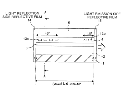
CA 02374274 2002-03-04
210428US-6029-1294-2
P-1529
TITLE OF THE INVENTION
SEMICONDUCTOR LASER DEVICE HAVING A DIFFRACTION GRATING ON
A LIGHT REFLECTION SIDE
BACKGROUND OF THE INVENTION
FIELD OF THE INVENTION
[0001) The present invention relates to a semiconductor laser device for use
in a
semiconductor laser module suitable as an excitation light source for a Raman
amplification
system, and more particularly to a semiconductor laser device having a
diffraction grating on a
light reflection side.
DISCUSSION OF THE BACKGROUND
[0002] With the proliferation of multimedia features on the Internet in the
recent years, there
has arisen a demand for larger data transmission capacity for optical
communication systems.
Conventional optical communication systems transmitted data on a single
optical fiber at a
single wavelength of 1310 nm or 1550 nm, which have reduced light absorption
properties for
optical fibers. However, in order to increase the data transmission capacity
of such single
fiber systems, it was necessary to increase the number of optical fibers laid
on a transmission
route which resulted in an undesirable increase in costs.
[0003] In view of this, there has recently been developed wavelength division
multiplexing
(WDM) optical communications systems such as the dense wavelength division
multiplexing
(DWDM) system wherein a plurality of optical signals of different wavelengths
can be
transmitted simultaneously through a single optical fiber. These systems
generally use an
Erbium Doped Fiber Amplifier (EDFA) to amplify the data light signals as
required for long
transmission distances. WDM systems using EDFA initially operated in the 1550
nm band
which is the operating band of the Erbium Doped fiber Amplifier and the band
at which gain
flattening can be easily achieved. While use of WDM communication systems
using the
EDFA has recently expanded to the small gain coefficient band of 1580 nm,
there has
1
CA 02374274 2002-03-04
nevertheless been an increasing interest in an optical amplifier that operates
outside the EDFA
band because the low loss band of an optical fiber is wider than a band that
can be amplified
by the EDFA; a Raman amplifier is one such optical amplifier.
[0004] In a Raman amplifier system, a strong pumping light beam is pumped into
an optical
transmission line carrying an optical data signal. As is known to one of
ordinary skill in the
art, a Raman scattering effect causes a gain for optical signals having a
frequency
approximately l3THz smaller than the frequency of the pumping beam. Where the
data signal
on the optical transmission line has this longer wavelength, the data signal
is amplified. Thus,
unlike an EDFA where a gain wavelength band is determined by the energy level
of an
Erbium ion, a Raman amplifier has a gain wavelength band that is determined by
a
wavelength of the pumping beam and, therefore, can amplify an arbitrary
wavelength band by
selecting a pumping light wavelength. Consequently, light signals within the
entire low loss
band of an optical fiber can be amplified with the WDM communication system
using the
Raman amplifier and the number of channels of signal light beams can be
increased as
compared with the communication system using the EDFA.
(0005] Although the Raman amplifier amplifies signals over a wide wavelength
band, the
gain of a Raman amplifier is relatively small and, therefore, it is preferable
to use a high
output laser device as a pumping source. However, merely increasing the output
power of a
single mode pumping source leads to undesirable stimulated Brillouin
scattering and increased
noises at high peak power values. Therefore, the Raman amplifier requires a
pumping source
laser beam having a plurality of oscillating longitudinal modes. As seen in
Figures 15A and
1 SB, stimulated Brillouin scattering has a threshold value P~h at which the
stimulated Brillouin
scattering is generated. For a pumping source having a single longitudinal
mode as in the
oscillation wavelength spectrum of Figure 15A, the high output requirement of
a Raman
amplifier, for example 300 mW, causes the peak output power of the single mode
to be higher
than P~, thereby generating undesirable stimulated Brillouin scattering. On
the other hand, a
pumping source having multiple longitudinal modes distributes the output power
over a
plurality of modes each having a relatively low peak value. Therefore, as seen
in Figure 1 SB,
a multiple longitudinal mode pumping source having the required 300 mW output
power can
be acquired within the threshold value P~h thereby eliminating the stimulated
Brillouin
scattering problem and providing a larger Raman gain.
[0006] In addition to the multiple longitudinal modes required for a pump
laser in a Raman
CA 02374274 2002-03-04
amplification system, the present inventors have recognized that it is
desirable that each of the
longitudinal modes has substantially the same threshold gain in order to
obtain the stable
mufti-mode oscillation.
(0007] In addition, because the amplification process in a Raman amplifier is
quick to occur,
when a pumping light intensity is unstable, a Raman gain is also unstable.
These fluctuations
in the Raman gain result in fluctuations in the intensity of an amplified
signal which is
undesirable for data communications. Therefore, in addition to providing
multiple
longitudinal modes, the pumping light source of a Raman amplifier must have
relatively
stable intensity.
[0008] Moreover, Raman amplification in the Raman amplifier occurs only for a
component
of signal light having the same polarization as a pumping light. That is, in
the Raman
amplification, since an amplification gain has dependency on a polarization,
it is necessary to
minimize an influence caused by the difference between a polarization of the
signal light
beam and that of a pumping light beam. While a backward pumping method causes
no
polarization problem because the difference in polarization state between the
signal light and
the counter-propagating pumping light is averaged during transmission, a
forward pumping
method has a strong dependency on a polarization of pumping light because the
difference in
polarization between the two co-propagating waves is preserved during
transmission.
Therefore, where a forward pumping method is used, the dependency of Raman
gain on a
polarization of pumping light must be minimized by polarization-multiplexing
of pumping
light beams, depolarization, and other techniques for minimizing the degree of
polarization
(DOP). In this regard it is known that the multiple longitudinal modes
provided by the
pumping light source help to provide this minimum degree of polarization.
[0009] Figure 16 is a block diagram illustrating a configuration of the
conventional Raman
amplifier used in a WDM communication system. In Figure 16, semiconductor
laser modules
182a through 182d, include paired Fabry-Perot type semiconductor light-
emitting elements
180a through 180d having fiber gratings 181 a through 181 d respectively. The
laser modules
182a and 182b output laser beams having the same wavelength via polarization
maintaining
fiber 71 to polarization-multiplexing coupler 61a . Similarly, the laser
modules 182c and
182d output laser beams having the same wavelength via polarization
maintaining fiber 71 to
polarization-multiplexing coupler 61b. Each polarization maintaining fiber 71
constitutes a
single thread optical fiber which has a fiber grating 181 a-181 d inscribed on
the fiber. The
3
CA 02374274 2002-03-04
polarization-multiplexing couplers 61a and 61b respectively output the
polarization-
multiplexed laser beams to a WDM coupler 62. These laser beams outputted from
the
polarization-multiplexing couplers 61a and 61b have different wavelengths.
[0010] The WDM coupler 62 multiplexes the laser beams outputted from the
polarization-
multiplexing couplers 61 a and 61b, and outputs the multiplexed light beams as
a pumping
light beam to external isolator 60, which outputs the beam to amplifying fiber
64 via WDM
coupler 65. Signal light beams to be amplified are input to amplifying fiber
64 from signal
light inputting fiber 69 via polarization-independent isolator 63, The
amplified signal light
beams are Roman-amplified by being multiplexed with the pumping light beams
and input to
a monitor light branching coupler 67 via the WDM coupler 65 and the
polarization-
independent isolator 66. The monitor light branching coupler 67 outputs a
portion of the
amplified signal light beams to a control circuit 68, and the remaining
amplified signal light
beams as an output laser beam to signal light outputting fiber 70. The control
circuit 68
performs feedback control of a light-emitting state, such as, an optical
intensity, of each of the
semiconductor light-emitting elements 180a through 180d based on the portion
of the
amplified signal light beams input to the control circuit 68 such that the
resulting Roman
amplification gain is flat over wavelength.
[0011] Figure 17 is an illustration showing a general configuration of a
conventional fiber
grating semiconductor laser module 182a -182d used in the conventional Roman
amplifier
system of Figure 16. As seen in Figure 17, semiconductor laser module 201
includes a
semiconductor light-emitting element (laser diode) 202 and an optical fiber
203. The
semiconductor light-emitting element 202 has an active layer 221 provided with
a light
reflecting surface 222 at one end thereof, and a light irradiating surface 223
at the other end.
Light beams generated inside the active layer 221 are reflected on the light
reflecting surface
222 and output from the light irradiating surface 223.
[0012] Optical fiber 203 is disposed on the light irradiating surface 223 of
the semiconductor
light-emitting element 222, and is optically coupled with the light
irradiating surface 223.
Fiber grating 233 is formed at a position of a predetermined distance from the
light irradiating
surface 223 in a core 232 of the optical fiber 203, and the fiber grating 233
selectively reflects
light beams of a specific wavelength. That is, the fiber grating 233 functions
as an external
resonator between the fiber grating 233 and the light reflecting surface 222,
and selects and
amplifies a laser beam of a specific wavelength which is then output as an
output laser beam
4
CA 02374274 2002-03-04
241.
[0013] While the conventional fiber grating semiconductor laser module 182a-
182d provides
the multiple longitudinal modes necessary for use in a Raman amplifier, the
fiber grating
module of Figure 17 is problematic in that residual reflection occurs at the
front facet 223 of
the laser diode202, and the module has a large value of relative intensity
noise (RIN) which
reflects large fluctuations in light intensity. As discussed above, this
fluctuation in the
pumping light intensity is undesirable for Raman amplification because it
could generate a
fluctuation in Raman gain which in turn causes the amplified signal to
fluctuate. The large
value RIN is especially undesirable for Raman amplifiers using a forward
pumping method,
where the signal light of weakened intensity and the pumping light of high
intensity propagate
in the same direction. Therefore, even though the conventional fiber grating
laser module
provides multiple longitudinal modes which allow a diminished degree of
polarization as
needed in a forward pumping method, the forward pumping method is not
frequently used
with the fiber grating module because of the high RIN of such module.
[0014] The mechanical structure of the fiber grating laser module also causes
instability of the
conventional pumping light source. Specifically, because the optical fiber 203
with fiber
grating 233 is laser-welded to the package, mechanical vibration of the device
or a slight shift
of the optical fiber 203 with respect to the light emitting element 202 could
cause a change in
oscillating characteristics and, consequently, an unstable light source. This
shift in the
alignment of the optical fiber 203 and light emitting element 202 is generally
caused by
changes in ambient temperature. In this regard, such changes in ambient
temperature also
cause small changes in oscillation wavelength selected by the fiber grating
233, further
contributing to instability of the pumping light source.
[0015] Yet another problem associated with the fiber grating laser module is
the high loss
caused by the need for an external isolator. In a laser module with a fiber
grating, an isolator
cannot be intervened between the semiconductor laser device and the optical
fiber because the
external cavity oscillation is governed by the reflection from the fiber
grating. That is, the
isolator would prevent the reflected light from the grating from returning to
the semiconductor
laser device. Therefore, the fiber grating laser module has a problem in that
it is susceptible to
reflection and easily influenced. Moreover, as seen in Figure 26, a Raman
amplifier system
using the fiber grating module must use external isolator 60. As is known in
the art, this
isolator presents a relatively high loss to the pumping light due to a
connection between the
CA 02374274 2002-03-04
collecting lens and output fiber of the external isolator.
SUMMARY OF THE INVENTION
(0016] Accordingly, one object of the present invention is to provide a laser
device and
method for providing a light source suitable for use as a pumping light source
in a Raman
amplification system, but which overcomes the above described problems
associated with a
fiber grating laser module.
[0017] Another aspect of the present invention is to provide a laser device
and method for
providing multiple oscillation modes having substantially the same threshold
gain.
[0018] The semiconductor device on which the method is based includes an
active layer
configured to radiate light, a light reflecting facet positioned on a first
side of the active layer,
a light emitting facet positioned on a second side of the active layer thereby
forming a
resonant cavity between the light reflecting facet and the light emitting
facet, and a partial
diffraction grating having a predetermined length and positioned on a light
reflecting side of
the resonator. The predetermined length of the partial diffraction grating is
selected such that
the semiconductor device emits a light beam having a plurality of longitudinal
modes within a
predetermined spectral width of an oscillation wavelength spectrum of the
semiconductor
device. The light reflecting facet may be configured to have a reflectivity of
no more than S%
or no less than 80%, and the light emitting facet may be configured to have a
reflectivity of no
more than S%.
[0019] According to one aspect of the invention, the predetermined length of
the partial
diffraction grating is set in relation to a length of the resonant cavity. In
this aspect, the
predetermined length of the partial diffraction grating is set to meet the
inequality:
Lgr <_ 1 /2 L,
where Lgr is the predetermined length of the partial diffraction grating and L
is the length of
the resonant cavity.
[0020] According to another aspect of the invention, the predetermined length
of the partial
diffraction grating is set in relation to a coupling coefficient of the
diffraction grating. In this
aspect, the predetermined length of the partial diffraction grating is set to
meet the inequality:
Ki~Lgr >_ 2,
CA 02374274 2002-03-04
where Ki is the coupling coefficient of the partial diffraction grating, and
Lgr is the length of
the partial diffraction grating. Also according to this aspect, the partial
diffraction grating has
a thickness tgr, a distance from the active layer dsp, and a diffraction
grating composition
Wavelength ~,gr, and at least one of the parameters tgr, dsp, and ~.gr is a
predetermined value
such that the coupling coefficient Ki is set in relation to the grating length
Lgr. The pitch of
the partial diffraction grating may be configured such that the center
wavelength is a shorter or
longer wavelength than a peak wavelength of the gain spectrum determined by
the active
layer.
[0021] The semiconductor device may also include another partial diffraction
grating
positioned on the light emitting side of the laser device. In this aspect, the
reflectivity of each
of the light reflecting and light emitting facets is no greater than 5%. In
addition, the laser
device and method of the present invention may be applied in a semiconductor
laser module,
optical fiber amplifier, Raman amplifier, or wavelength division multiplexing
system.
BRIEF DESCRIPTION OF THE DRAWINGS
[0022] A more complete appreciation of the invention and many of the attendant
advantages
thereof will be readily obtained as the same becomes better understood by
reference to the
following detailed description when considered in connection with the
accompanying
drawings, wherein:
[0023] Figure 1 is a broken perspective view showing a general configuration
of a
semiconductor laser device according to an embodiment of the present
invention;
[0024] Figure 2 is a vertical sectional view in the longitudinal direction of
the semiconductor
laser device shown in Figure 1;
[0025] Figure 3. is a cross sectional view of the semiconductor laser device,
taken along the
line A-A of the semiconductor laser device shown in Figure 2;
[0026] Figure 4 is a graph showing the multiple oscillation longitudinal mode
output
characteristics of a diffraction grating semiconductor laser device in
accordance with one
embodiment of the present invention;
[0027] Figure 5 is a diagram showing the relation of oscillation wavelength
and threshold
gain of a laser device in accordance with the present invention;
CA 02374274 2002-03-04
[0028] Figure 6 is a diagram showing the selection level characteristic
relating to the
oscillation wavelength spectrum of a device in accordance with the present
invention;
[0029] Figures 7A-7C are graphs showing the selection level characteristics of
an oscillation
wavelength spectrum under various coupling coefficients and diffraction
grating lengths;
[0030] Figure 8 is a diagram showing various physical parameters of a
semiconductor laser
device according to the present invention;
[0031) Figure 9 is a sectional view at the reflective film side of a
semiconductor laser device
according to an embodiment of the present invention;
(0032] Figure 10 is a diagram illustrating the concept of setting the
wavelength oscillation
spectrum in relation to the gain spectrum of the active layer in accordance
with an
embodiment of the present invention;
(0033) Figure 11 is a vertical sectional view illustrating a configuration of
a semiconductor
laser module in accordance with the present invention;
[0034] Figure 12 is a block diagram illustrating a configuration of a Raman
amplifier in which
polarization dependency is canceled by polarization-multiplexing of pumping
light beams
output from two semiconductor laser devices, in accordance with an embodiment
of the
present invention;
[0035] Figure 13 is a block diagram illustrating a configuration of a Raman
amplifier in which
polarization dependency is canceled by depolarizing a pumping light beam
output from a
single semiconductor laser device using polarization maintaining fibers as a
depolarizer, in
accordance with an embodiment of the present invention;
[0036) Figure 14 is a block diagram illustrating a general configuration of a
WDM
communication system in which the Raman amplifier shown in Figure 12 or 13 is
used;
(0037] Figures 15A and 15B are graphs showing the relationship of laser beam
output powers
with respect to a single oscillation longitudinal mode and a plurality of
oscillation longitudinal
modes, and a threshold value of the stimulated Brillouin scattering;
[0038] Figure 16 is a block diagram illustrating a general configuration of a
conventional
Raman amplifier; and
[0039] Figure 17 is a diagram showing a configuration of a semiconductor laser
module used
in the Raman amplifier shown in Figure 16.
CA 02374274 2002-03-04
DETAILED DESCRIPTION OF THE PREFERRED EMBODIMENTS
[0040] Refernng now to the drawings wherein like elements are represented by
the same
reference designation throughout, and more particularly to Figures 1, 2 and 3
thereof, there is
shown a semiconductor laser device for providing a light source suitable for
use as a pumping
light source in a Raman amplification system in accordance with an embodiment
of the
present invention. Figure 1 is a broken perspective view showing a general
configuration of a
semiconductor laser device according to an embodiment of the present
invention. Figure 2 is
a vertical sectional view in the longitudinal direction of the semiconductor
laser device shown
in Figure 1, and Figure 3 is a cross sectional view of the semiconductor laser
device, taken
along the line A-A in Figure 2.
[0041] The semiconductor laser device 20 of Figures 1-3 includes an n-InP
substrate 1 having
an n-InP buffer layer 2, an active layer 3, a p-InP spacer layer 4, a p-InP
cladding layer 6, and
an InGaAsP cap layer 7 sequentially stacked on a face (100) of the substrate
1. Buffer layer 2
serves both as a buffer layer by the n-InP material and an under cladding
layer, while the
active layer 3 is a graded index separate confinement multiple quantum well
(GRIN-SCH-
MQV~ and has a compression strain. A diffraction grating 13a of a p-InGaAsP
material is
periodically formed within the p-InP spacer layer 4 along a portion the entire
length of active
layer 3. The diffraction grating 13a of the embodiment of Figure 1 has a film
thickness of 20
nm, a pitch of 220 nm, and selects a laser beam having a central wavelength of
1480 nm, to be
emitted by the semiconductor laser device 20. It is to be noted however, that
the present
invention is applicable to wavelengths of 1100nm to 1550nm As best seen in
Figure 3, the p-
InP spacer layer 4 having the diffraction grating 13, the GRIN-SCH-MQW active
layer 3, and
the upper part of the n-InP buffer layer 2 are processed in a mesa strip
shape. The sides of the
mesa strip are buried by a p-InP blocking layer 8 and an n-InP blocking layer
9 formed as
current blocking layers. In addition, a p-side electrode 10 is formed on the
upper surface of
InGaAsP cap layer 7, and an n-side electrode 11 is formed on the back surface
of n-InP
substrate 1.
[0042] As seen in Figure 2, reflective film 14 having high reflectivity of,
for example, 80% or
more is formed on a light reflecting end surface that is one end surface in
the longitudinal
direction of the semiconductor laser device 20. Antireflection coating 15
having low light
reflectivity of, for example, S% or less, is formed on a light irradiating end
surface opposing
the light reflecting end surface of semiconductor laser device 20. The
reflective film 14 and
9
CA 02374274 2002-03-04
the antireflection coating 1 S form a light resonator within the active region
3 of the
semiconductor laser device 20. A light beam generated inside the GRIN-SCH-MQW
active
layer 3 of the light resonator is reflected by the reflective film 14 and
irradiated as an output
laser beam via the antireflection coating 15.
[0043] As also seen in Figure 2, the resonator length L may be 800p,m to
3200~tm as will be
further described below, but is 1200pm in the preferred embodiment. In the
embodiment of
Figure 2, the diffracting grating 13a is SOOpm and extends along only a
portion of the length
of the resonator and is placed so as to extend from the reflective coating 14.
That is, the
diffraction grating 13a is a partial grating positioned on the light
reflection side of the device
20. As used herein, the phrase "positioned on the light reflection side" means
that the distance
from the antireflective filin 15 to a grating element of grating 13a closest
to the film 15 is
larger than the distance from the reflective filin 14 to the grating element
of grating 13a
closest to the film 14. As also shown in Figure 2, the present invention may
also include a
grating 13b extending from the light emission side reflective film 15 of the
laser device. The
diffraction grating 13b is shown in phantom to indicate that it is not
necessary for the present
invention as will be discussed below. The gratings 13a and 13b distribute and
feed back the
light produced in the active layer as a laser beam that is emitted mainly from
the exit side of
the reflective film 15. In this regard, the diffraction gratings 13a and 13b
are preferably
placed so that the end grating element is in contact with its respective
reflective film 14 or 1 S.
However, due to inaccuracies in the cleaving position as will be further
described below, the
diffraction gratings 13a and 13b may be positioned apart from the reflective
film 15 as shown
in Figure 2, as long as the diffraction gratings still perform their
respective functions.
[0044] Thus, as seen in the embodiment of Figures 1-3, the present invention
provides a
partial diffraction grating positioned on a light reflection side of the
semiconductor laser
device 20. The present inventors have realized that such an integrated
diffraction grating
contained within the semiconductor laser device provides several advantages
over external
fiber grating laser modules such as the one described with respect to Figure
17.
[0045] First, the semiconductor laser module illustrated in Figure 17 provides
a light source
with high RIN which is contrary to the requirements of a Raman amplifier as
discussed above.
Refernng again to Figure 17, the present inventors have discovered that the
fiber grating
semiconductor laser module 201 ( 182a through 182d in Figure 16) has a large
RIN due to
multiple resonance. The multiple resonance is the resonance that occurs
between the external
to
CA 02374274 2002-03-04
fiber grating 233 and the light reflecting surface 222, and the resonance that
occurs between
the reflecting surface 222 and the light emitting surface 223 of the
semiconductor laser
emitting element 202. That is, due to the long interval between the fiber
grating 233 and the
semiconductor light-emitting element 202, stable Raman amplification cannot be
performed.
However, since the semiconductor laser device 20 of the present invention
provides a laser
beam irradiated from the low reflection coating 15 directly as an excitation
light source of the
Raman amplifier without using an external fiber grating, the RIN is smaller.
As a result, the
fluctuation of the Raman gain becomes smaller and a stable Raman amplification
can be
performed in systems using an integrated diffraction grating semiconductor
laser device in
accordance with the present invention. Another reason about low RIN is as
follows.
According to the iGM, an isolation can be set in a package of a LD module.
Then the
isolation can be located near the LD.
[0046] Moreover, because of the low RIN level, the integrated grating
semiconductor laser
device of the present invention is not constrained to a backward pumping
method when used
in a Raman amplification system as with fiber grating semiconductor laser
modules.
Applicants have recognized that the backward pumping method is most frequently
used in
present fiber grating Raman amplifier systems because the forward pumping
method, in which
a weak signal light beam advances in the same direction as a strong excited
light beam, has a
problem in that fluctuation-associated noises of pumping light are easy to be
modulated onto
the signal. As discussed above, the semiconductor laser device of the present
invention
provides a stable pumping light source for Raman amplification and therefore
can easily be
adapted to a forward pumping method.
(0047] The mechanical stability problems of the semiconductor laser module
illustrated in
Figure 17 are also diminished by the present invention. Since the resonator of
the diffraction
grating device is not physically separated from the semiconductor laser device
but
monolithically integrated therein, the semiconductor laser device of this
first embodiment
does not experience a variation of the oscillating characteristic of a laser
caused by mechanical
vibration or change in ambient temperature and can acquire a stable light
output and Raman
gain. Moreover, as the diffraction grating of the present invention is
internal to the
semiconductor device, the temperature of the grating is controlled by the
temperature control
unit that provides temperature control for the semiconductor device. This not
only eliminates
the affects of ambient temperature changes on the oscillation wavelength
selected by the
m
CA 02374274 2002-03-04
grating, but also provides a mechanism for controlling the oscillation
wavelength of a multiple
mode laser device in accordance with the present invention as will be further
described below.
While the integrated diffraction grating device of the present invention
provides the above-
described advantages over the fiber grating laser module, the primary use of
the present
invention is as a pumping source for a Raman amplifier. Therefore, the
integrated diffraction
grating device of the present invention must also provide multiple
longitudinal mode
operation. Despite the fact that conventional integrated grating devices
provided only single
mode operation suitable for a signal light source, the present inventors have
discovered that
multiple mode operation suitable for a pumping light source for Raman
amplification can be
provided by an integrated diffraction grating device.
[0048] Figure 4 shows the multiple oscillation longitudinal mode output
characteristics of a
diffraction grating semiconductor laser device of the present invention. As
seen in this figure,
the oscillation wavelength spectrum 30 provides multiple longitudinal modes,
for example 31,
32, and 33, separated by a wavelength interval ~~,. As the integrated
diffraction grating of the
laser device of the present invention selects a longitudinal mode by its Bragg
wavelength,
Figure 4 also shows the predetermined spectral width w of the oscillation
spectrum 30 as
defined by of half power points hp of the oscillation spectrum. The
predetermined spectral
width w is a predetermined spectral bandwidth, which defines a portion of the
wavelength
oscillation spectrum that includes the laser operating modes. Thus, while
Figure 4 shows the
predetermined spectral width w as the full width at half maximum power (FWHM),
it is to be
understood that the predetermined spectral width w may be defined by any width
on the
oscillation spectrum 30. For example, another known way to define the
predetermined
spectral width is by the l Odb down from maximum power points of the
oscillation wavelength
spectrum 30. It is clear from this description that the number of laser
operating modes may
change for a given oscillation wavelength spectrum depending on how the
predetermined
spectral width w is defined. Thus, as recognized by the present inventors, in
order to provide
the multiple oscillation longitudinal mode characteristics required to reduce
stimulated
Brillouin scattering in a Raman amplifier, an integrated diffraction grating
laser device of the
present invention must provide a plurality of oscillation longitudinal modes
within the
predetermined spectral width w of the oscillation wavelength spectrum 30.
[0049] Moreover, the present inventors have recognized that the number of
longitudinal
12
CA 02374274 2002-03-04
modes included in the predetermined spectral width w should be at least three,
as shown by
modes 31, 32, and 33 of Figure 4. As discussed above, Raman amplification
systems using a
forward pumping method presents a problem in the resulting gain is dependent
on the
polarization of the incident pumping light. This dependency is canceled by
performing
polarization-multiplexing of pumping light beams output from two of the
semiconductor laser
devices 20, or by depolarizing a pumping light beam output from a single
semiconductor laser
device using polarization maintaining fibers as a depolarizer (these
alternative embodiments
are shown in Figures 12 and 13 respectively which will be further described
below). In the
latter case, the angle of the polarization axis of the polarization
maintaining fiber against the
emitted light from semiconductor laser device is approximately 45 degrees.
With this
configuration, an output of the laser device having a single polarization can
obtain a random
polarization by propagating a minimum distance through a polarization
maintaining fiber. In
general, the more the number of the oscillation longitudinal modes is
increased, the shorter the
length of the polarization maintaining fiber can be. Particularly, when the
number of the
oscillation longitudinal modes is more than three, preferably four or five,
the coherence length
of the laser light becomes shorter and the length of polarization maintaining
fiber necessary
for depolarizing the laser light becomes markedly short. Thus, it becomes
easier to obtain a
laser light of low degree of polarization (DOP) which is spectral for reducing
the polarization
dependency of a Raman amplifier, making it more feasible to replace 2 laser
modules which
are polarization-multiplexed with a single laser module with higher power and
to thereby
reduce the cost of lasers as well as polarization maintaining fibers.
[0050] In order to achieve the desired plurality of oscillation modes within
the predetermined
spectral width of the oscillation profile, the present inventors have
recognized that the
predetermined spectral width w and/or the wavelength interval 0~, may be
manipulated.
However, a Rart~an amplification system poses limits on the values of the
wavelength interval
tl~, and predetermined spectral width w of the oscillation wavelength spectrum
30. With
regard to the wavelength interval 0~,, the present inventors have determined
that this value
should 0.1 nm or more as shown in Figure 4. This is because, in a case in
which the
semiconductor laser device 20 is used as a pumping light source of the Raman
amplifier, if the
wavelength interval 0~, is 0.1 nm or more, it is unlikely that the stimulated
Brillouin scattering
is generated. With regard to the predetermined spectral width w of the
oscillation wavelength
13
CA 02374274 2002-03-04
profile 30, if the predetermined spectral width of the oscillation wavelength
is too wide, the
coupling loss by a wavelength-multiplexing coupler becomes larger. Moreover, a
noise and a
gain variation are generated due to the fluctuation of the wavelength within
the spectrum
width of the oscillation wavelength. Therefore, the present inventors have
determined that the
predetermined spectral width w of the oscillation wavelength spectrum 30
should be 3 nm or
less as shown in Figure 4, and is preferably 2 nm or less.
[0051] In general, a wavelength interval 0~, of the longitudinal modes
generated by a
resonator of a semiconductor device can be represented by the following
equation:
0~.= ~ 2/(2~n~L),
where n is the effective refractive index, ~,o is the oscillation wavelength,
and L is a length of
the resonator defined by the reflection coating 14 and antireflection coating
15 as discussed
with respect to Figures 1-3 above. From this equation it is seen that,
neglecting refractive
index n which has only a marginal affect on 0~, , the longer the resonator
length is, the
narrower the wavelength interval 07~ becomes, and selection conditions for
oscillating a laser
beam of the signal longitudinal mode becomes stricter. However, in order to
provide the
desired plurality of longitudinal modes within a predetermined spectral width
w of 3nm or
less, the resonator length L cannot be made too short. For example, in the
diffraction grating
device of Figures 1-3 where the oscillation wavelength 7~o is 1480 nm and the
effective
refractive index is 3.5, the wavelength interval 07~ of the longitudinal mode
is approximately
0.39 nm when the resonator length is 800 p,m . When the resonator length is
800 ~,m or
more, it is easy to obtain a plurality of operating modes and higher output
power. However,
the resonator length L must not be made so long that the required wavelength
interval of 0.1
nm cannot be achieved. Returning to the example of Figures 1-3 when the
resonator length is
3200 Vim, the wavelength interval 0~, of the longitudinal mode is
approximately 0.1 nm.
(0052] Thus, for a semiconductor laser device having an oscillation wavelength
~.a of 1100
nm to 1550 nm, and in particular 1480 nm, and an effective refractive index of
3.5, the
resonator cavity length L must be approximately within the range of 800 to
3200 ~m as
indicated in Figure 2. It is noted that an integrated diffraction grating
semiconductor laser
device having such a resonator length L was not used in the conventional
semiconductor laser
14
CA 02374274 2002-03-04
devices because single longitudinal mode oscillation is difficult when the
resonator length L is
800 p,m or more. However, the semiconductor laser device 20 of the present
invention, is
intentionally made to provide a laser output with a plurality of oscillation
longitudinal modes
included within the predetermined spectral width w of the oscillation
wavelength spectrum by
actively making the resonator length L 800 pm or more. In addition, a laser
diode with such a
long resonator length is suitable to get high output power.
[0053] The objective of providing a plurality of operating modes within a
predetermined
spectral width w of the oscillation profile 30 may also be achieved by
widening the
predetermined spectral width w of the oscillation profile 30. In general, the
predetermined
spectral width w of the oscillation wavelength spectrum 30 is varied by
changing a coupling
coefficient Ki and/or a grating length Lg of the diffraction grating.
Specifically, assuming a
fixed coupling coefficient xi and a predetermined spectral width w defined by
the FWHM
points, where the grating length Lg of the resonator is decreased, the
predetermined spectral
width w is increased thereby allowing a greater number of longitudinal modes
to occupy the
predetermined spectral width w as laser operating modes. In this regard, it is
noted that
conventional integrated grating devices used only a full length grating
structure. This is
because these conventional devices provided only single mode operation in
which it was
undesirable to increase predetermined spectral width. The present inventors
have discovered
that shortening the grating is useful in providing multiple mode operation.
[0054] As described above, a laser device to be used as an excitation source
for a Raman
amplifier should contain a plurality of oscillation longitudinal modes within
a predetermined
spectral width w of the laser device's wavelength oscillation profile. Methods
and devices for
providing a plurality of oscillation longitudinal modes within a predetermined
spectral width
w of the laser device's wavelength oscillation profile are disclosed in U.S.
Patent Application
No. 09/832,885 filed on April 12, 2001, the entire contents of which are
incorporated herein
by reference. The objective of providing multiple oscillation modes within a
predetermined
width is generally achieved by adjusting the device cavity length to
manipulate the
wavelength interval and adjusting the coupling coefficient and/or grating
length to manipulate
the spectral width. However, the present inventors have discovered that where
a shortened
diffraction grating is placed on the reflective coating side of the laser
device as shown in
Figures 1-3, the relationship between the diffraction grating length Lgr and
the coupling
CA 02374274 2002-03-04
coefficient xi has particular importance in obtaining a plurality of stable
oscillation modes.
(0055) First, the present inventors recognized that a plurality of stable
oscillation modes can
be obtained where a nearly flat oscillation threshold gain is achieved by the
laser device. The
threshold gain is a gain necessary for oscillating; the lower the threshold
gain is, the easier it is
for oscillation, and the higher the threshold gain, the less easier is the
oscillation. Figure 5 is a
diagram showing the relation of oscillation wavelength and threshold gain of
the
semiconductor laser device shown in Figure 1 to Figure 3. Each plot in Figure
5 represents a
wavelength mode of the laser device. Where the corresponding threshold gain
for a
wavelength mode is relatively low, the possibility of oscillation for that
mode is high. Thus,
Figure 5 includes plots P 1 to P4 of four wavelength modes that are lower in
the threshold gain
as compared with other plots, and therefore produce four oscillation
longitudinal modes.
Where the corresponding threshold gain for a wavelength mode is relatively
high, the
possibility of oscillation for that mode is low. Thus, the wavelength modes
other than P1, P2,
P3, and P4 in Figure 5 each have a relatively high threshold gain and
therefore result in non-
oscillation modes. It is noted that the term "non-oscillation modes" is
intended to indictae
that the wavelength modes do not have large gain in order to oscillate.
[0056] As shown in Figure S, plots P 1 to P4 of the oscillation modes are
formed near the
Bragg wavelength 1480 nm corresponding to period 220 nm of the diffraction
grating 13a. As
seen in the figure, the value ~b represents the threshold gain difference
between the oscillation
mode P2 having the least threshold gain and the oscillation mode P4 having the
greatest
threshold gain. That is, each oscillation mode plot P1-P4 has a threshold gain
difference from
other oscillation mode plots of less than 0b. On the other hand, the value Da
represents the
threshold gain difference between the oscillation mode P4 having the greatest
threshold gain
of the oscillation modes P1-P4, and the non-oscillation mode having the least
threshold gain
among the non-oscillation modes.
(0057] The present inventors have recognized that in order to provide a
plurality of stable
oscillation modes the threshold gain difference 0a between oscillation
longitudinal mode and
non-oscillation longitudinal mode is preferred to be larger. That is, if the
threshold gain
difference ~a between oscillation longitudinal mode and non-oscillation
longitudinal mode is
small, as the injection current increases, oscillation begins and the
oscillation spectrum width
becomes broader, and the optical output characteristic may kink due to a mode
hopping
16
CA 02374274 2002-03-04
caused by generation of a new mode. On the other hand, the threshold gain
difference 0b
between oscillation longitudinal modes is preferred to be smaller. That is,
when the threshold
gain difference Ob is small, each oscillation longitudinal mode oscillates
always in the same
condition.
[0058] More specifically, the present inventors have discovered that a 0a
value 1.5 cm' or
more, and a 0b value of 1 cm'' or less will ensure that the plurality of
oscillation longitudinal
modes oscillate at nearly the same level and a stable output is provided.
Moreover, these
values will ensure a high level of selectivity among oscillation and non-
oscillation modes.
Figure 6 is a diagram showing the selection level characteristic relating to
the oscillation
wavelength spectrum by the diffraction grating 13a. Characteristic 40 shown in
Figure 6
shows the characteristic of the selection level relating to the oscillation
wavelength in the case
of setting of characteristic of threshold gain relating to the oscillation
wavelength as shown in
Figure 5. The characteristic selection level of the oscillation wavelength is
a flat and high
selection level in a band of 2 nm, centered at 1480 nm. The present inventors
have conducted
several experiments to determine the impact of coupling coefficient xi and the
diffraction
grating length Lgr on obtaining the high and flat selection level curve of
Figure 6.
[0059] Specifically, Figures 7A - 7C are graphs showing the selection level
characteristics of
an oscillation wavelength spectrum under various coupling coefficients Ki and
diffraction
grating lengths Lgr. Figure 7A is a graph showing the changes in wavelength
oscillation
profile where the coupling coefficient Ki is held constant and the diffraction
grating Lgr is
changed from a small value to a large value. As seen in this figure, the
oscillation wavelength
spectrum showing the selection level relating to the oscillation wavelength
shows a steep hill
profile of a relatively narrow spectrum width when the diffraction grating
length Lgr is small.
However, as the grating length Lgr is increased, the wavelength oscillation
profile is swollen
until the final selection level is a high and flat characteristic as also
shown.
[0060] Figure 7B is a graph showing the changes in wavelength oscillation
profile where the
diffraction grating length Lgr is held to a relatively short length of about
100 Vim, for example,
while the coupling coefficient Ki is changed from a small value to a large
value. As seen in the
figure, where the coupling coefficient xi is a small value, a steep hill
profile of a relatively
narrow spectrum width is achieved. However, as the coupling coefficient Ki is
increased, the
entire hill profile is swollen without formation of high selection level. In
contrast, Figure 7C is
17
CA 02374274 2002-03-04
a graph showing the changes in wavelength oscillation profile where the
diffraction grating
Lgr is held to a relatively long length of about 500 pm, for example, while
the coupling
coefficient of is changed from a small value to a large value. Where Ki is a
small value in
Figure 7C, the spectrum width is relatively narrow with a high and flat
selection level.
Moreover, as the coupling coefficient Ki is increased, spectrum width is
broadened while
maintaining its high flat selectivity characteristic.
[0061 ] Based on the results represented in Figures 7A-7C, the present
inventors determined
that by setting the diffraction grating length Lgr to 500 ~m and the coupling
coefficient Ki to
40 cm ', a flat and high selectivity characteristic oscillation wavelength
selection curve having
a width of 2 nm is achieved. That is, where the the product of the diffraction
grating length
Lgr and the coupling coefficient Ki is Ki *Lg=2, the desired selectivity of
the oscillation curve
can be achieved. Moreover, by setting the product of the diffraction grating
length Lgr and
the coupling coefficient Ki at of*Lg>_2, two or more oscillation longitudinal
modes can be
maintained at nearly the same oscillation level.
[0062] Figure 8 shows various physical parameters of a semiconductor laser
device according
to the present invention. The figure shows a layout relationship between the
GRIN-SCH-
MQW active layer 3 and the diffraction grating 13, with the GRIN-SCH-MQW
active layer 3
having a construction in which the MQW layer 3b is sandwiched by the GRIN-SCH
layers 3a
and 3c. As seen in Figure 8, the length of the diffraction grating 13 is
represented by "Lg"
(p,m), the thickness of the diffraction grating is represented by "tgr" (nm),
and the distance
between the diffraction grating 13 and the GRIN-SCH layer 3a is represented by
"dsp" (nm).
In addition, "~,gr" (gym) represents the diffraction grating composition
wavelength, which
corresponds to the band gap energy of a material forming the diffraction
grating 13. The
present inventors have recognized that the parameters tgr, ~,gr, and dsp
affect the coupling
coefficient value Ki of a device according to the present invention. Thus, by
changing these
physical parameters and the length Lg, a Ki*Lg value of 2 or more can be
achieved.
[0063] Aside from the diffraction grating length Lgr being an important factor
in providing a
flat and highly selective oscillation wavelength spectrum, the present
inventors have also
realized that the parameter Ki is important to determining the output level of
the laser.
Specifically, the present inventors have discovered that despite the improved
selectivity of a
relatively large Lgr value as discussed with respect to Figure 7C, where the
diffraction grating
is
CA 02374274 2002-03-04
13a extends into the light emitting side of the laser device, the reflectivity
of the grating
decreases thereby decreasing the light output at the light emission side of
the laser device.
That is, to improve reflective properties of the diffraction grating 13a
placed on the light
reflecting side, the diffraction grating should be kept to no more than 1/2 of
the resonator
length L. Thus, the present inventors have discovered that, to optimize
selectivity of the
wavelength oscillation spectrum while also maintaining output efficiency, the
diffraction
grating 13a should be approximately equal to 1/2 the resonator length L.
[0064] In addition to controlling the grating length Lgr of the grating 13a to
improve light
output efficiency of the device, the present inventors have determined that
placing a
diffraction grating 13b on the side of the light emission facet of the laser
device even further
improves the light output of the laser device 20. Specifically, where the exit
side reflective
film 15 has the reflectivity of 5% as mentioned above, the diffraction grating
13b is not
needed. However, the diffraction grating 13b may be provided in order to
guarantee that at
least part of the laser beam may be returned to the resonator at the exit
side. In this regard, the
length Lgf of the diffraction grating 13b is enough as far as the diffraction
grating 13b is
present, and it is provided at the exit side as far as possible so that the
reflectivity due to the
diffraction grating 13b may be lower. The present inventors have discovered
that in a device
having diffraction gratings 13a and 13b, the output of the laser beam emitted
from the
reflective film 15 side has a value of 20 or more as compared with the output
of the laser beam
emitted from the rear reflective film 14. Thus, a semiconductor laser device
of high laser
beam output efficiency is realized.
[0065] As yet another means of improving light output efficiency, the present
inventors have
realized that the reflective value of the reflective film 14 affects the light
output efficiency of a
laser device having a partial diffraction grating on the light reflecting side
of the device.
Figure 9 is a sectional view at the reflective film side of a semiconductor
laser device
according to an embodiment of the present invention. The laser device includes
a partial
diffraction grating 13a on the light reflecting side as described with respect
to Figures 1-3, and
a reflective film 24 similar to the reflective film 14 of Figures 1-3. As
discussed above, the
grating 13a and the film 24 provide reflection of the laser light generated by
the active layer of
the device. Thus, as shown in Figure 9, a portion of the light within the
resonator of the laser
device 20 is reflected by the grating 13a as "L1," with the remaining portion
of the light
reaching the film 24. Of the light reaching the film 24, a portion "L2" is
reflected back into
19
CA 02374274 2002-03-04
the resonator by the film 24, and a portion "LO" exits the film 24 to the
exterior of the laser
device.
(0066] Where the reflecting film is 80% or more as described in Figures 1-3
above, most of
the light reaching the reflective film will be reflected back into the cavity
of the laser device as
light portion L2. This light L2 may be either in phase or out of phase with
the light L1
reflected by the grating 13a. Where the light L2 is in phase with the light
L1, no problem
occurs; however, where L1 and L2 are out of phase, the laser beam L1 is
attenuated by the
light L2 to an extent depending on the phase deviation between these signals.
For example,
where the lights L1 and L2 are exactly opposite phase, the light L2 will
cancel a portion of the
light L1.
[00b7] Whether the light portions L1 and L2 are in phase is determined by a
cleaving position
of the laser device. The cleavage is formed when a plurality of semiconductor
laser devices
formed in a matrix shape on a semiconductor substrate such as a wafer are cut
into individual
laser devices. The wafer is first cut into strips, or laser bars, which form a
series of
semiconductor devices that have their sides in the length direction aligned
adjacent to each
other. The cleavage occurs when the laser bar is cut into individual laser
devices. When the
cleavage is made at accurate cleavage positions, the light L2 is caused to be
in phase with the
light L1. However, when the cleavage position is shifted from the accurate
cleavage position,
the light L2 will be out of phase with the light L 1. However, the cleavage
position cannot be
easily controlled with the result that the cutting position often causes out
of phase reduction in
the light to be emitted by the laser device. This results in inferior laser
devices which may be
scrapped. Thus, in order to provide high yield in the manufacture of such
devices,
complicated high precision cleaving must be performed.
[0068) The present inventors have recognized that with a device having the
diffraction grating
on the reflective side of the device, most of the light within the resonator
is reflected by the
grating 13a. This is particularly true where the grating 13a is not more than
1/2 L as described
above. Therefore, in reflective side grating devices, the reflective
properties of the reflective
film 24 is not needed to keep most of the light within the resonator. Thus, it
is desirable to
lower the reflectivity property of the film 24 so that light L2 which may
result in out of phase
losses is allowed to escape the device as light LO. Specifically, according to
the present
invention, the reflectivity of film 24 is preferably 5% or less. That is, of
the light reaching the
film 24, 95% of the light is allowed to escape as light LO and only 5% of the
light is reflected
CA 02374274 2002-03-04
as light L2. Thus, if a reflected light of reverse phase is caused due to
cleavage position, a
drop of laser beam output is negligible and a stable laser output can be
obtained. In this
regard, it may be contemplated that the reflective film 24 is not necessary at
all. However, the
reflectivity of an uncoated cleavage side is generally high. Therefore, the
output from the
reflective film 24 to outside is securely realized by coating with the
reflective film 24 at a low
reflectivity of 5% or less.
[0069] In the embodiments of the invention previously described, a static
characteristic of the
gain spectrum of the active layer has been assumed. In the case of actual
laser oscillation,
however, the gain spectrum of the active layer 3 generally moves to a longer
wavelength with
an increase in driving current. The present inventors have determined that
this dynamic
characteristic of the gain spectrum of the active layer may be used to provide
a laser device
having specific characteristics for a given device application. Figure 10 is a
diagram
illustrating the concept of setting the wavelength oscillation spectrum in
relation to the gain
spectrum of the active layer in order to obtain a laser device having
characteristics for a
specific device application. As seen in this figure, the graph includes an
oscillation
wavelength spectrum 40, a gain spectrum 41 having a peak gain wavelength 41 a,
and a gain
spectrum 42 having a peak gain wavelength 42a. The gain spectrums 41 and 42
represent the
gain spectrum of an active layer in two different semiconductor devices.
[0070] In the case of the gain spectrum active layer 41, as indicated above,
this gain spectrum
41 is shifted to the longer wavelength side, by about several nanometers,
along with an
increase of the driving current. However, the oscillation wavelength spectrum
40 of the
diffraction grating 13a is set at the longer wavelength side as compared with
the peak
wavelength 41 a of the gain spectrum 41. Therefore, as the driving current
increases, the peak
wavelength 41 a is taken into the oscillation wavelength spectrum 40, so that
a stable laser
output of high output is obtained.
(0071 ] When the gain spectrum determined by the active layer 3 itself is gain
spectrum 42,
this gain spectrum 42 is also shifted to the longer wavelength side, by about
several
nanometers along with the increase of the driving current. However, in this
case, the
oscillation wavelength spectrum 40 of the diffraction grating 13a is set at
the shorter
wavelength side as compared with the peak wavelength 42a of the gain spectrum
42.
Therefore, as the driving current is increased, peak wavelength 42a is moved
outside of the
oscillation wavelength spectrum 40 thereby increasing the differential gain of
the laser device.
21
CA 02374274 2002-03-04
This increase in differential gain decreases the relative intensity noise
(RIN) so that a laser
beam of low noise level can be produced. . Another reason about low RIN is as
follows.
According to the iGM, an isolation can be set in a package of a LD module.
Then the isolation
can be located near the LD.
[0072] Therefore, where a stabilized high output laser beam is needed, the
oscillation
wavelength spectrum 40 should be set at the longer wavelength side of the gain
spectrum of
the active layer itself, and where laser beam of low noise level is required,
the oscillation
wavelength spectrum 40 should be set at the shorter wavelength side of the
gain spectrum of
the active layer itself. This process of setting the oscillation wavelength
spectrum 40 in
relation to the peak wavelength of the gain spectrum of the active layer is
achieved by
adjusting the pitch of the partial grating. That is, by adjusting the pitch of
the grating
elements of the diffraction grating 13a, the center wavelength of the
oscillation wavelength
spectrum 40 can be set to a desired wavelength.
[0073] Figure 11 is a vertical sectional view illustrating the configuration
of a semiconductor
laser module having a semiconductor laser device according to the present
invention. The
semiconductor laser module 50 includes a semiconductor laser device 51, a
first lens 52, an
internal isolator 53, a second lens 54 and an optical fiber 55. Semiconductor
laser device 51 is
an integrated grating device configured in accordance with any of the above-
described
semiconductor laser devices and a laser beam irradiated from the semiconductor
laser device
51 is guided to optical fiber 55 via first lens 52, internal isolator 53, and
second lens 54. The
second lens 54 is provided on the optical axis of the laser beam and is
optically coupled with
the optical fiber 55.
[0074] The present inventors have recognized that, in the semiconductor laser
module 50
having the semiconductor laser device 51 of the present invention, since the
diffraction grating
is formed inside the semiconductor laser device 51, internal isolator 53 can
be intervened
between the semiconductor laser device 51 and the optical fiber 55. This
provides an
advantage in that reflected return light beams by other optical parts or from
the external of the
semiconductor laser nodule 50 are not re-inputted in the resonator of the
laser device 51. Thus,
the oscillation of the semiconductor laser device 51 can be stable even in the
presence of
reflection from outside. Moreover, placing the internal isolator 53 between
the laser device 51
and optical fiber 55 does not introduce loss to the laser module. As is known
in the art, the
loss of an isolator is primarily in the area of a collecting lens which
focuses the light beam
22
CA 02374274 2002-03-04
onto a fiber at the output of the isolator material. The loss is caused by the
coupling between
this output lens and an output optical fiber. However, by using an internal
isolator 53, the
second lens 54 of the laser module 50 provides the function of the output lens
of the isolator.
Since the second lens 54 is necessary to the laser module SO even without the
internal isolator,
the internal isolator 53 does not introduce any power lass into the laser
module 50. In fact,
use of the internal isolator reduces the loss of Raman amplifier system as
will be fiwther
described below. Another advantage provided by the Internal isolator 53 is
that it provides
stable isolation characteristics. More specifically, since internal isolator
53 is in contact with
the Pettier module 58, the internal isolator 53 is held at a constant
temperature and therefore
does not have the fluctuating isolation characteristics of an external
isolator which is typically
at ambient temperature.
[0075] A back face monitor photo diode 56 is disposed on a base 57 which
functions as a heat
sink and is attached to a temperature control device 58 mounted on the metal
package 59 of
the laser module 50. The back face monitor photo diode 56 detects a light
leakage from the
reflection coating side of the semiconductor laser device 51. The temperature
control device
58 is a Pettier module. Although current (not shown) is given to the Pettier
module 58 to
perform cooling and heating by its polarity, the Pettier module 58 functions
mainly as a cooler
in order to prevent an oscillation wavelength shift by the increase of
temperature of the
semiconductor laser device 51. That is, if a laser beam has a longer
wavelength compared
with a desired wavelength, the Pettier element 58 cools the semiconductor
laser device 51 and
controls it at a low temperature, and if a laser beam has a shorter wavelength
compared with a
desired wavelength, the Pettier element 58 heats the semiconductor laser
device 51 and
controls it at a high temperature. By performing such a temperature control,
the wavelength
stability of the semiconductor laser device can be improved. Alternatively, a
thermistor 58a
can be used to control the characteristics of the laser device. If the
temperature of the laser
device measured by a thermistor 58a located in the vicinity of the laser
device 51 is higher, the
Pettier module 58 cools the semiconductor laser device 51, and if the
temperature is lower, the
Pettier module 58 heats the semiconductor laser device S 1. By performing such
a temperature
control, the wavelength and the output power intensity of the semiconductor
laser device are
stabilized.
[0076] Yet another advantage of the laser module 50 using the integrated laser
device
according to the present invention 15 that the Pettier module can be used to
control the
23
CA 02374274 2002-03-04
oscillation wavelength of the laser device. As described above, the wavelength
selection
characteristic of a diffraction grating is dependant on temperature, with the
diffraction grating
integrated in the semiconductor laser device in accordance with the present
invention, the
Pettier module 58 can be used to actively control the temperature of the
grating and,
therefore, the oscillation wavelength of the laser device.
[0077] Figure 12 is a block diagram illustrating a configuration of a Raman
amplifier used in
a WDM communication system in accordance with the present invention. In Figure
12,
semiconductor laser modules 60a through 60d are of the type described in the
embodiment of
Figure 11. The laser modules 60a and 60b output laser beams having the same
wavelength
via polarization maintaining fiber 71 to polarization-multiplexing coupler.
Similarly, laser
beams outputted by each of the semiconductor laser modules 60c and 60d have
the same
wavelength, and they are polarization-multiplexed by the polarization-
multiplexing coupler
61b. Each of the laser modules 60a through 60d outputs a laser beam having a
plurality of
oscillation longitudinal modes in accordance with the present invention to a
respective
polarization-multiplexing coupler 61a and 61b via a polarization maintaining
fiber 71.
[0078] Polarization-multiplexing couplers 61a and 61b output polarization-
multiplexed laser
beams having different wavelengths to a WDM coupler 62. The WDM coupler 62
multiplexes
the laser beams outputted from the polarization multiplexing couplers 61 a and
61b, and
outputs the multiplexed light beams as a pumping light beam to amplifying
fiber 64 via WDM
coupler 65. Thus, as seen in Figure 12, a Raman amplifier using a laser module
in accordance
with the present invention does not include an external isolator such as
isolator 60 of Figure
16. Therefore, the loss associated with the external isolator, as discussed
above, is eliminated
from the Raman amplifier system of Figure 12. Signal light beams to be
amplified are input
to amplifying fiber 64 from signal light inputting fiber 69 via polarization-
independent
isolator 63. The amplified signal light beams are Raman-amplified by being
multiplexed with
the pumping light beams and input to a monitor light branching coupler 67 via
the WDM
coupler 65 and the polarization-independent isolator 66. The monitor light
branching coupler
67 outputs a portion of the amplified signal light beams to a control circuit
68, and the
remaining amplified signal light beams as an output laser beam to signal light
outputting fiber
70.
[0079] The control circuit 68 controls a light-emitting state, for example, an
optical intensity,
of each of the semiconductor light-emitting elements 180a through 180d based
on the portion
24
CA 02374274 2002-03-04
of the amplified signal light beams input to the control circuit 68. Moreover,
control circuit
68 performs feedback control of a gain band of the Raman amplification such
that the gain
band will be flat over wavelength.
[0080] The Raman amplifier described in Figure 12 realizes all of the
advantages of the
semiconductor laser device as previously described. For example, although the
Raman
amplifier illustrated in Figure 12 is the backward pumping method, since the
semiconductor
laser modules 60a through 60d output stable pumping light beams, a stable
Raman
amplification can be performed whether the Raman amplifier is the forward
pumping method
or the bi-directional pumping method.
[0081] The Raman amplifier can be constructed by wavelength-multiplexing of a
plurality of
pumping light which are not polarization-multiplexed. That is, the
semiconductor laser
module of the present invention can be used in a Raman amplifier where the
polarization-
multiplexing of pumping light is not performed. Figure 13 is a block diagram
illustrating a
configuration of a Raman amplifier in which polarization dependency is
canceled by
depolarizing a pumping light beam output from a single semiconductor laser
device using
polarization maintaining fibers as a depolarizes, in accordance with an
embodiment of the
present invention. As seen in this figure, laser modules 60a and 60c are
directly connected to
WDM coupler 62 via a polarization maintaining fiber 71. In this configuration,
the angle of
the polarization axis of the polarization maintaining fiber against the
emitted light from
semiconductor laser device is approximately 45 degrees. As mentioned above,
since at least 3
longitudinal modes are included in the predetermined spectral width of the
output spectrum of
the laser light, the coherence length of the laser light becomes shorter and
the length of
polarization maintaining fiber necessary for depolarizing the laser light
becomes markedly
short. Thus, it becomes easier to obtain a laser light of low degree of
polarization (DOP)
which is spectral for reducing the polarization dependency of a Raman
amplifier. Therefore,
the laser device of the present invention provides a further advantage in that
it is possible to
substitute 2 units of laser modules which are polarization-multiplexed (as
shown in Figure 12)
for one unit of depolarized laser module of greater power (as shown in Figure
13), without
deteriorating DOP and while obtaining a corresponding reduction in costs.
[0082] The Raman amplifier illustrated in Figures 12 and 13 can be applied to
the WDM
communication system as described above. Figure 14 is a block diagram
illustrating a general
configuration of the WDM communication system to which the Raman amplifier
shown in
CA 02374274 2002-03-04
either Figure 12 or Figure 13 is applied.
[0083] In Figure 14, optical signals of wavelengths ~,, through ~,~ are
forwarded from a
plurality of transmitter Tx, through Tx ~ to multiplexing coupler 80 where
they are wavelength-
multiplexed and output to optical fiber 85 line for transmission to a remote
communications
unit. On a transmission route of the optical fiber 85, a plurality of Raman
amplifiers 81 and
83 corresponding to the Raman amplifier illustrated in Figure 11 are disposed
amplifying an
attenuated optical signal. A signal transmitted on the optical fiber 85 is
divided by an optical
demultiplexer 84 into optical signals of a plurality of wavelengths ~,,
through ~, ", which are
received by a plurality of receivers Rx, through Rx n. Further, an ADM
(AddlDrop
Multiplexer) may be inserted on the optical fiber 85 for inserting and
removing an optical
signal of an arbitrary wavelength.
[0084] Obviously, numerous modifications and variations of the present
invention are
possible in light of the above teachings. It is therefore to be understood
that within the scope
of the appended claims, the invention may be practiced otherwise than as
specifically
described herein. For example, the present invention has been described as a
pumping light
source for the Raman amplification, it is evident that the configuration is
not limited to this
usage and may be used as an EDFA pumping light source of the oscillation
wavelength of
980nm and 1480nm. Moreover, while the identity of coupling coefficient of the
diffraction
gratings 13a, 13b has not been mentioned, it may be either same or different.
When the
coupling coefficients are same, the manufacturing process of semiconductor
laser device is
easier, and when the coupling coefficients are different, the degree of
freedom of design is
increased.
26