Note: Descriptions are shown in the official language in which they were submitted.
CA 02374337 2002-01-17
WO 01/07689 PCT/US00/20357
TELLURIUM-CONTAINING NANOCRYSTALLINE MATERIALS
TECHNICAL FIELD
The invention relates to tellurium-containing nanocrystalline materials, and
to
methods for making such materials.
BACKGROUND
Semiconductor nanocrystallites having radii smaller than the bulk exciton Bohr
radius constitute a class of materials intermediate between molecular and bulk
forms of
matter. Quantum confinement of both the electron and hole in all three
dimensions leads
to an increase in the effective band gap of the material with decreasing
crystallite size.
Consequently, both the optical absorption and emission of nanocrystallites
shift to the
blue (i.e., to higher energies) as the size of the crystallite gets smaller.
Bawendi and co-workers have described a method of preparing monodisperse
semiconductor nanocrystallites by pyrolysis of organometallic reagents
injected into a hot
coordinating solvent (J. Am. Chem. Soc., 115:8706 (1993)). This permits
temporally
discrete nucleation and results in the controlled growth of macroscopic
quantities of
nanocrystallites. The particle size distribution can be refined by size
selective
precipitation. The narrow size distribution of nanocrystallites can allow the
particles to
have narrow spectral width emissions. These techniques can yield excellent
results in the
production of selenium-containing II-VI semiconductor nanocrystallites.
SUMMARY
The invention provides methods of synthesizing telluride semiconductor
nanocrystallites. The nanocrystallites can have high quantum efficiencies and
can have
narrow size distributions. The telluride semiconductors have relatively
smaller band gaps
than their selenide and sulfide analogs, and can expand the range of colors
available using
II-VI photoluminescent nanocrystallites further into the far red range of the
spectrum. In
particular, cadmium telluride nanocrystallites can emit in wavelengths
sufficiently long to
make them suitable for use in multicolor detection schemes for whole blood
diagnostics,
where emission wavelengths of at least 630 nm can be preferred.
In one aspect, the invention features a nanocrystallite including a core of
MTe,
where M is cadmium, zinc, magnesium, mercury, or mixtures thereof. The core
can have
-1-
CA 02374337 2002-01-17
WO 01/07689 PCT/US00/20357
an overcoating on a surface of the core. The overcoating can be a
semiconductor having
a composition different from the core.
In another aspect, the invention features a nanocrystallite including MTe that
can
photoluminesce with a quantum efficiency of at least 20%.
In another aspect, the invention features a method of manufacturing
nanocrystallites by injection of an M-containing compound, M being cadmium,
zinc,
magnesium, mercury, or mixtures thereof, and a Te-containing compound of the
form
z
~
Te P Z'
Z"
where at least one of Z, Z', and Z" is an amide. Preferably, two of Z, Z', and
Z" are,
independently, amides, and more preferably three of Z, Z', and Z" are,
independently,
amides. The mixture is heated to grow the nanocrystallites. The heating can be
controlled in such a way that the growth is controlled. The M-containing
compound and
a Te-containing compound can be premixed, or M and Te can be incorporated into
different positions of a single molecule. The M-containing compound and the Te-
containing compound can be injected sequentially or simultaneously. Additional
M-
containing compound, additional Te-containing compound, or a mixture thereof,
can be
added to the mixture during heating. An overcoating can be grown on a surface
of the
nanocrystallite. The nanocrystallites can be separated by size selective
precipitation. An
amine can be added to the mixture during size selective precipitation. The Te-
containing
compound can include a tris(dialkylamino)phosphine telluride. The Te-
containing
compound can have a boiling point of at least 200 C, preferably 250 C, and
more
preferably 280 C, at one atmosphere.
In another aspect, the invention features a Te-containing compound of the form
z
~
Te P\ Z'
Z"
where at least one of Z, Z', and Z" is an amide, and a method of preparing a
Te-
containing compound including contacting P(Z)(Z')(Z") with Te.
The nanocrystallite can have a quantum efficiency of emission of at least 30%,
40%, 50%, 60%, or 70%. The quantum efficiency can be as high as 75%, 80%, 90%,
95% or 99%. The quantum efficiency can be between 20 and 99%, preferably
between
-2-
CA 02374337 2002-01-17
WO 01/07689 PCT/US00/20357
30 and 99%, more preferably between 40 and 95%, and most preferably between 70
and
95%. The nanocrystallite can be a member of a size-selected population having
no more
than a 15% RMS deviation from mean diameter, preferably 10% RMS deviation or
less,
and more preferably 5% RMS deviation or less. CdTe nanocrystallites can
photoluminesce and can have emission wavelengths in the range of 580 to 770
nm,
preferably 550 to 780 nm, and more preferably 435 to 800 nm. The
nanocrystallite can
photoluminesce with a full-width at half maximum (FWHM) of 70 nm or less,
preferably
45 nm or less, more preferably 20 nm or less, and most preferably 15 nm or
less for a
single nanocrystallite.
The details of one or more embodiments of the invention are set forth in the
accompanying drawings and the description below. Other features, objects, and
advantages of the invention will be apparent from the description and
drawings, and from
the claims.
DESCRIPTION OF DRAWINGS
FIG. 1(a) is a diagram depicting a method according to the invention.
FIG. 1(b) is a drawing depicting structures of two precursors for synthesis of
CdTe nanocrystals.
FIGS. 2(a)-2(c) are graphs depicting the UV/vis absorption spectra and the x-
ray
diffraction spectra of CdTe nanocrystals prepared with TOPTe and HPPTTe.
FIGS. 3(a) and 3(b) are graphs depicting the development of the UV/vis
absorption spectra during nanocrystallite synthesis.
FIG. 4 is a graph depicting the evolution of photoluminescence during
nanocrystallite synthesis.
FIG. 5 is a graph depicting shows the accessible absorption spectra for CdTe
nanocrystallites.
FIG. 6 is a graph depicting the evolution of the photoluminescence of a dilute
solution of nanocrystallites exposed to air.
FIG. 7 is a graph depicting the evolution of the photoluminescence of a dilute
solution of nanocrystallites in an air-free environment.
FIG. 8 is a graph depicting the intensity lifetimes of CdTe nanocrystallites
stored
under air and under nitrogen.
-3-
CA 02374337 2008-01-22
FIG. 9 is a graph depicting the evolution of the photoluminescence as a
function
of temperature.
FIG. 10 is a TEM image of telluride semiconductor nanocrystallites.
FIG. 11 is a series of graphs depicting size histograms for several
nanocrystallite
syntheses.
FIG. 12 is a graph depicting the dependence of the photoluminescence on
diameter for CdTe nanocrystallites.
FIG. 13 is a graph depicting x-ray diffraction spectra for three sizes of CdTe
nanocrystallites.
FIG. 14 is a graph depicting the band gaps of several bulk II-VI
semiconductors.
FIG. 15 is a graph depicting the emission spectra of a series of sizes of CdTe
nanocrystallites.
DETAILED DESCRIPTION
Tellurium-containing nanocrystallites can be produced by injection of an M-
containing compound and a Te-containing compound into a hot coordinating
solvent,
followed by growth and annealing of the nanocrystallites. The nanocrystallites
can
include CdTe, ZnTe, MgTe, HgTe, or alloys thereof. By proper selection of
precursor
composition and stoichiometry, telluride semiconductor photoluminescent
nanocrystallites having quantum efficiencies as high as 70% can be produced.
Improved telluride nanocrystallites can be produced by varying the precursor
compounds and the precursor stoichiometry from that described in U.S. Patent
U.S. Patent No. 6,322,901.
Cadmium telluride nanocrystallites made by the methods
described in U.S. Patent No. 6,322,901 using dimethyl cadmium (Me2Cd) and
trioctylphosphine telluride (TOPTe) as precursors exhibit inefficient
photoluminescence,
having quantum efficiencies of less than 1%. The telluride-containing
nanocrystallites
produced using a Te-containing compound including an amino group can be
prepared
having quantum efficiencies as high as 70%, more than threefold higher than
the quantum
efficiency of 20% reported for colloidal CdTe nanocrystallites (J. Phys. Chem.
1993(97):11999-12003). The quantum efficiency of nanocrystallites can be
further
enhanced by overcoating a core nanocrystallite with a layer of a second
semiconductor
material (e.g., ZnS or ZnSe overcoated CdTe cores).
-4-
CA 02374337 2002-01-17
WO 01/07689 PCT/USOO/20357
Tellurium-containing nanocrystallites are obtained using a high temperature
colloidal growth process, preferably followed by size selective precipitation.
The high
temperature colloidal growth process can be accomplished by rapidly injecting
an
appropriate combination of an M-containing compound and Te-containing compound
into
a hot coordinating solvent to produce a temporally discrete homogeneous
nucleation and
controlling the growth of the nuclei into nanocrystallites. Injection of
reagents into the
hot reaction solvent results in a short burst of homogeneous nucleation. This
temporally
discrete nucleation is attained by a rapid increase in the reagent
concentration upon
injection, resulting in an abrupt supersaturation, which is relieved by the
formation of
nuclei and followed by growth on the initially formed nuclei. The partial
depletion of
reagents through nucleation and the sudden temperature drop associated with
the
introduction of room temperature reagents prevents further nucleation.
The solution then may be gently heated to reestablish the solution
temperature.
Gentle reheating allows for growth and annealing of the nanocrystallites. The
higher
surface free energy of the small crystallites makes them less stable with
respect to
dissolution in the solvent than larger crystallites. The net result of this
stability gradient is
the slow diffusion of material from small particles to the surface of large
particles
("Ostwald ripening"). In addition, the reagents remaining in the coordinating
solvent may
contribute to growth; this effect may be encouraged by feeding additional
reagents to the
solution during growth. Growth and ripening of this kind result in a highly
monodisperse
colloidal suspension from systems which may initially be highly polydisperse.
The
process of slow growth and annealing of the nanocrystallites in the
coordinating solvent
that follows nucleation results in uniform surface derivatization and regular
core
structures. Both the average size and the size distribution of the
crystallites in a sample
are dependent on the growth temperature. The growth temperature necessary to
maintain
steady growth increases with increasing average crystal size. As the size
distribution
sharpens, the temperature may be raised to maintain steady growth. The growth
period
may be shortened significantly by using a higher temperature or by adding
additional
precursor materials. The overall process is shown schematically in FIG. 1(a).
Size distribution during the growth stage of the reaction can be estimated by
monitoring the absorption line widths of the particles. Modification of the
reaction
temperature in response to changes in the absorption spectrum of the particles
allows the
maintenance of a sharp particle size distribution during growth. Reactants can
be added
-5-
CA 02374337 2002-01-17
WO 01/07689 PCT/USOO/20357
to the nucleation solution during crystal growth to grow larger crystals. The
photoluminescence (PL) spectra of the nanocrystallites can be tuned
continuously over
maximum emission wavelengths from 550 to 780 nm, complementing the available
wavelengths for nanocrystallites having CdSe cores. The wavelength of maximum
emission can be tuned by stopping the growth a particular average size of
nanocrystallite.
The particle size distribution may be further refined by size selective
precipitation.
The M-containing compound can be an organometallic compound, such as an
alkyl-M compound. For example, the M-containing compound can be MRQ wherein M
is Cd, Zn, Hg or Mg, and R and Q are, independently, alkyl, alkenyl, aryl,
cycloalkyl, or
cycloalkenyl. Preferred examples include dialkyl Cd, dialkyl Zn, dialkyl Hg or
dialkyl
Mg.
The Te-containing compound can be a stable phosphine telluride, preferably a
tris
amido phosphine telluride. The Te-containing compound can have formula
z
~
Te P` Z'
z"
At least one of Z, Z', and Z" can be an amide. Preferably, two of Z, Z', and
Z" are
amides. The remaining groups of Z, Z', and Z" can be alkyl, alkenyl, aryl,
cycloalkyl, or
cycloalkenyl, or derivatives thereof. More preferably, each of Z, Z', and Z"
is an amide.
Each of Z, Z', and Z" can have the formula -N(A)(A'), where each of A and A',
independently, is alkyl, alkenyl, aryl, cycloalkyl, or cycloalkenyl, or a
derivative thereof.
Preferably, each of Z, Z', and Z" is a dialkyl amide. Each alkyl can be a
lower alkyl. The
Te-containing compound has a boiling point of at least 200 C. One suitable Te-
containing compound is hexapropyiphosphorustriamide telluride (HPPTTe). HPPTTe
produces unexpectedly high quantum efficiency nanocrystallites as compared
nanocrystallites prepared from trioctylphosphine telluride (TOPTe). The
structures of
HPPTTe and TOPTe are shown in FIG. 1(b).
Alternatively, a single compound containing M and Te can be used as both the M-
containing compound and the Te-containing compound. An example of such a
compound is a Te-containing compound in which one of Z, Z', and Z" includes a
dialkyl
M moiety.
Alkyl is a branched or unbranched saturated hydrocarbon group of 1 to 100
carbon atoms, preferably 1 to 30 carbon atoms, such as methyl, ethyl, n-
propyl, isopropyl,
-6-
CA 02374337 2002-01-17
WO 01/07689 PCT/US00/20357
n-butyl, isobutyl, t-butyl, octyl, decyl, tetradecyl, hexadecyl, eicosyl,
tetracosyl and the
like, as well as cycloalkyl groups such as cyclopentyl, cyclohexyl and the
like. The term
"lower alkyl" includes an alkyl group of 1 to 20 carbon atoms, preferably 2 to
8 carbon
atoms.
Alkenyl is a branched or unbranched hydrocarbon group of 2 to 100 carbon atoms
containing at least one carbon-carbon double bond, such as ethenyl, n-
propenyl,
isopropenyl, n-butenyl, isobutenyl, t-butenyl, octenyl, decenyl, tetradecenyl,
hexadecenyl,
eicosenyl, tetracosenyl and the like. The term "lower alkenyl" includes an
alkenyl group
of 2 to 20 carbon atoms, preferably 2 to 8 carbon atoms, containing one -C=C-
bond.
Optionally, an alkyl, or alkenyl chain can contain 1 to 6 linkages selected
from the
group consisting of -0-, -S-, -M- and -NR- where R is hydrogen, lower alkyl or
lower
alkenyl.
Aryl is a monovalent aromatic hydrocarbon radical consisting of one or more
fused rings in which at least one ring is aromatic in nature, which can
optionally be
substituted with one or more of the following substituents: hydroxy, cyano,
alkyl, alkoxy,
thioalkyl, halo, haloalkyl, hydroxyalkyl, nitro, amino, alkylamino, and
dialkylamino,
unless otherwise indicated.
Cycloalkyl is reference to a monovalent saturated carbocyclic radical
consisting of
one or more rings, which can optionally be substituted with one or more of the
following
substituents: hydroxy, cyano, alkyl, alkoxy, thioalkyl, halo, haloalkyl,
hydroxyalkyl,
nitro, amino, alkylamino, and dialkylamino, unless otherwise indicated.
Cycloalkenyl includes reference to a monovalent unsaturated carbocyclic
radical
consisting of one or more rings and containing one or more carbon-carbon
double bonds,
which can optionally be substituted with one or more of the following
substituents:
hydroxy, cyano, alkyl, alkoxy, thioalkyl, halo, haloalkyl, hydroxyalkyl,
nitro, amino,
alkylamino and dialkylamino, unless otherwise indicated.
The absolute quantum efficiency of the nanocrystallites was as high as 70%.
The
average quantum efficiency of a group of 15 nanocrystallite samples was 60 5%,
attesting to the reproducibility of the method. FIG. 2 displays UV/vis
absorption spectra
from CdTe preparations using (a) TOPTe and (b) HPPTTe. Initial absorption
spectra
from each reaction show similar qualitative features. Nucleation produces a
bimodal
distribution of sizes, with the smaller species quickly dissolving into
feedstock for the
larger nanocrystallites. After three hours of stirring at 290 C, each reaction
has
-7-
CA 02374337 2008-01-22
01997-276W01
effectively the same absorption spectrum. As monitored by absorption
spectroscopy,
both reactions appear the same. However, the quantum efficiency of the CdTe
synthesized with TOPTe is only 1%, whereas the quantum efficiency of CdTe
produced
with HPPTTe is 55%.
Without wishing to be bound by any particular explanation, it is believed that
the
strong electron-donating properties of the amide groups in the HPPTTe are at
least
partially responsible for the improvement in nanocrystal quality. Te-
containing
compounds having one or two amide groups can produce significantly improved
quantum
efficiencies for telluride nanocrystallites compared to trialkyl phosphine
telluride
compounds. A suitable Te-containing compound should be stable at reaction
temperature
(e.g., having a boiling point of at least 200 C).
The interchangeability of the spectra of FIGS. 2(a) and 2(b) suggests that
UV/vis
absorption spectroscopy is not sensitive to the differences which would
explain the PL
intensities. TEM and XRD analysis also did not reveal any substantial
differences
between the two species, as shown by the XRD spectra in FIG. 2(c).
The nanocrystallites can be overcoated with a coating of a semiconductor
material. For example, ZnS, ZnSe or CdSe overcoatings can be grown on CdTe
nanocrystallites.
The telluride nanocrystallites can be suitable for a variety of applications,
including those disclosed in co-pending and commonly owned U.S. Patent No.
6,251,303
filed September 18, 1998, U.S. Patent No. 6,326,144 filed September 24, 1998,
U.S. Patent No. 6,617,583 filed September 24, 1998 and U.S. Patent No.
6,803,719 filed
July 9, 1999. In particular, a light-emitting device as described in Example 3
of U.S.
Patent 6,803,719 constructed using CdTe nanocrystallites produces a very
intense red
light
EXAMPLES
Synthesis of CdTe nanocrystallites
Unless otherwise noted, all reactions were carried out in a dry nitrogen
atmosphere using a glovebox or standard Schlenk techniques. HPLC grade
solvents used
for size selective precipitation were purged of dissolved oxygen by bubbling
with
nitrogen for 5 minutes. Trioctylphosphine (TOP, 95%) was used as received from
Fluka.
-8-
CA 02374337 2002-01-17
WO 01/07689 PCT/US00/20357
Tellurium shot (99.999%, low oxide) was used as received from Alfa/Aesar. Hexa-
n-
propyl phosphorous triamide (HPPT, 97%, Lancaster) was vacuum distilled,
collecting
the fraction boiling between 83-103 C at 0.55 Torr. Trioctylphosphine oxide
(TOPO,
90%, Strem) was dried under vacuum (-0.5 Torr) for 1 hour. Dimethyl cadmium
(99+%,
Strem) was purified by vacuum transfer.
A stock solution of hexapropylphosphorustriamide telluride (HPPTTe) was
prepared by adding 6.38 g tellurium shot to 45.00 g HPPT and stirring until
dissolved (1-
2 days). 20g TOPO was dried under vacuum (-0.5 Torr) at 180 C for 1 hour,
then filled
with N2 and heated to 350 C. In a N2 atmosphere glovebox a solution
containing 50 L
CdMe2 (0.69 mmol), 0.35 mL HPPTTe stock (0.35 mmol), and 12 mL TOP was mixed
very well and loaded into a syringe. This solution was smoothly injected (-0.5
sec) into
the vigorously stirring TOPO, which immediately turned red and cooled to 270
C. When
the reaction solution was sampled within 20 seconds of injection, the initial
UV/vis
spectrum displayed a bimodal distribution of sizes, with absorption features
at 435 and
560 nm. Subsequent absorption spectra showed no evidence of a high energy
peak, with
the first absorption feature now peaked at 580 nm. The temperature was raised
to 290 C
and the sample was grown to the desired wavelength. The flask was then cooled
to - 60
C and mixed with 10 mL butanol. This solution can be stored (under nitrogen)
for at
least 6 months without noticeable decrease in quantum efficiency.
Nanocrystallites were isolated in air by a modified size selective
precipitation with
acetonitrile. The reaction solution prepared above was mixed with an
additional 10 mL
butanol. Acetonitrile was added until the mixture became turbid. Upon sitting
for a few
minutes the solution separated into two layers. The colorless hydrophilic
phase was then
removed and discarded. The clear red hydrophobic phase was mixed with
approximately
one third its original volume of butanol. The process of adding acetonitrile
until turbidity
and separating layers was repeated until a powder or very thick oil was
obtained. Freshly
prepared CdTe nanocrystallites isolated in this fashion are moderately soluble
in hexane
and extremely soluble in tetrahydrofuran (THF). Addition of a small amount of
TOP
(-1% vol) helped preserve the luminescence intensity of the size selected
material.
Yields of crude CdTe ranged from 50 mg (small sizes) to 75 mg (large sizes) of
dry
powder.
-9-
CA 02374337 2002-01-17
WO 01/07689 PCT/US00/20357
CdTe nanocrystallites were synthesized using a method that employed a 1M
hexapropyl phosphorous triamide telluride (HPPTTe) solution as the
chalcogenide-
containing compound. Distillation of the HPPT before use was found to
significantly
increase the quantum efficiency of the samples. Purification of CdMe2 by
vacuum
transfer gave more consistent results than filtration through 0.2 m PTFE
membrane.
Also, a cadmium rich preparation was found to give better results. The optimum
Cd:Te
injection solution ratio for the conditions of this example was determined
empirically to
be 2:1. FIG. 3 displays UV/vis absorption spectra at various times during CdTe
synthesis. FIG. 3(a) highlights the early stages of the synthesis. The bottom
spectrum of
FIG. 3(a), taken 10 seconds after injection when the temperature had fallen to
280 C,
shows that the reaction solution contained a bimodal distribution of sizes.
Well defined
features at 2.23 eV (566 nm) and 2.84 eV (437 nm) are clearly visible. A
species
absorbing at or near 435 nm can be synthesized by performing the injection at
200 C or
below. These are the smallest nanocrystallites to display a nanocrystallite-
like absorption
and appear to be the 435 nm-absorbing CdTe species equivalent to 410 nm
absorption
CdSe. Two minutes into the reaction the concentration of this 435 nm-absorbing
CdTe
species was greatly reduced, and at 7 minutes there was no trace of this
species. These
435 nm-absorbing CdTe species did not appear to be growing. No spectral
feature has
been observed between 435 and 550 nm during reactions performed under similar
initial
conditions. Instead, the 435 nm-absorbing CdTe species appeared to be
dissolving as the
absorption of the larger nanocrystallites grew and sharpened. Growth of the
larger
particles at the expense of the smaller ones is an Ostwald ripening mechanism
and is to be
expected given the difference in size (-35 A versus - 15 A). The observation
of this
mechanism would not be noteworthy, except for the fact that in this case the
dissolving
species is the 435 nm-absorbing CdTe species . The other semiconductor
materials in this
family, CdS and CdSe, do not show similar behavior in their growth pattern.
Characterization of Nanocrystallites
UV/visible absorption spectroscopy of CdTe nanocrystallites in hexane was
performed on an HP 8453 diode array spectrometer with 1 nm resolution.
Fluorescence
measurements were made using a SPEX Fluorolog-2 spectrofluorometer which
consisted
of two double monochromators with 2400 grooves/inch gratings blazed at 500 nm
and
photomultiplier tube (R928) detector. CdTe samples were dissolved in either
hexane or
- 10-
CA 02374337 2002-01-17
WO 01/07689 PCTIUSOO/20357
THF with -1% TOP in a 1 cm quartz cuvette and diluted until the absorbance of
the first
feature was below 9.3. Spectra were obtained in front face geometry and were
corrected
for the wavelength dependence of the optics and detector by multiplication
with a suitable
correction factor file (MCOR1097.SPT).
FIG. 3(b) displays absorption spectra of aliquots taken from a single
synthesis of
CdTe. A well defined first absorbing state is visible in all spectra,
indicating that the
growth is controlled. FIG. 4 shows the corresponding photoluminescence (PL)
emission
spectra for the same reaction. Spectra have been standardized relative to a
methanol
solution of rhodamine 640 (quantum efficiency = 100%) so as to accurately
reflect the
emission intensity at various points during the reaction, a relationship which
is plotted in
the inset FIG. 4(b). Three features stand out in FIG. 4. First, the quantum
efficiency
improved over time. This result suggests the importance of an annealing
effect. For
small nanocrystallites it can be experimentally difficult to separate thermal
annealing
from particle growth. Second, all emission occurred at the band edge. There
was no low
energy (or deep trap) light detected for this size range. The spectral window
was
examined down to 1.18 eV (1050 nm) using a CCD detector without observing deep
trap
emission. More importantly, CdTe samples as small as - 35 A diameter displayed
no
deep trap emission, whereas similarly sized CdS and CdSe luminescence spectra
generally contain at least 20% deep trap emission. The third aspect of the
emission is
simply the sheer magnitude of the quantum efficiency. The nanocrystals used to
generate
FIG. 4 reaches 55%, but samples as high as 70% have been prepared.
FIG. 5 presents absorption spectra illustrating the range of CdTe sizes that
have
been produced by this method. Any size/energy between the two extremes can be
produced. Slight adjustments in starting material concentration and/or
reaction
temperature should enable the lower diameter limit to be reduced below its
present value
of - 44 A.
The stability with respect to flocculation and PL intensity of dilute
solutions of
CdTe nanocrystallites were qualitatively less than those of CdSe because the
CdTe
nanocrystallites are air sensitive. FIG. 6 shows the PL of a dilute hexane
solution of 53 A
diameter CdTe as the emission decreases over time in air. The insert of FIG. 6
plots
intensity versus time over the entire experiment. The emission intensity is
effectively
zero after 2.5 hours. At this point the solution is also quite turbid. A
comparative
experiment was conducted under nitrogen and the results are shown in FIG. 7.
Even after
-11-
CA 02374337 2002-01-17
WO 01/07689 PCT/US00/20357
39 hours the fluorescence intensity has only fallen to just under half the
initial value.
Also, after 12 hours the air-free solution becomes very turbid. The solution
phase
"lifetimes" of the PL intensities are compared in FIG. 8. Results presented
here show that
the useable lifetime of CdTe nanocrystallites, particularly in dilute
solutions, can be
greatly extended by keeping the nanocrystallites in an inert atmosphere. While
manipulating more concentrated solutions in air, for example, during size
selective
precipitation, PL does not appear to be greatly diminished. Long term storage
of the
nanocrystallites under nitrogen, or another inert gas, can help maintain the
quantum
efficiency.
The PL of the CdTe nanocrystallites is temperature dependant. A reaction
apparatus containing already synthesized 50 A diameter CdTe nanocrystal growth
solution was assembled in the fluorometer sample chamber and attached to a
nitrogen
source. The temperature of the system was equilibrated for ten minutes and
then a
spectrum was obtained. FIG. 9 displays the PL spectrum of the nanocrystallites
at a range
of temperatures. The hysteresis in FIG. 9 is believed to be due to growth
and/or
decomposition that occurred during the latter half of the experiment.
Transmission electron microscopy (TEM) provides valuable information about the
size, shape, and distribution of the CdTe nanocrystal samples. Collecting a
large
population of measurements ensured statistically meaningful data. A JEOL
2000FX
transmission electron microscope operating at 200 kV was used to obtain high
resolution
images of the CdTe nanocrystallites. 400 mesh copper grids with an ultralight
coating of
amorphous carbon (Ladd) served as substrates. Solutions of CdTe
nanocrystallites were
prepared by size selecting once with acetonitrile, washing the powder once
with
methanol, dissolving in THF, and diluting until the absorbance at the first
state was
between 0.3-0.6 in a lcm cuvette. One drop of this solution was placed onto a
carbon
grid and, after 10 seconds had elapsed, the excess solution was wicked away
with a tissue.
An objective aperture was used to improve contrast while still being able to
image the
(111) lattice spacing, the most intense ring in the diffraction pattern.
Measurements were
performed on images taken between 210,000-410,000X magnification. Microscope
magnification readings were calibrated using the d-spacing of the (111) planes
measured
by X-ray diffraction (3.742 A). The instrumental magnification reading was
found to be
systematically low in this range; all measurements given herein are multiplied
by 1.15 to
reflect accurate values.
-12-
CA 02374337 2008-01-22
CdTe samples were carefully size selected once with acetonitrile as described
in
U.S. Patent No. 6,322,901. The powder was
washed once with methanol and then dissolved in THF. Solution concentration
was
adjusted to deposit a submonolayer coverage of nanocrystallites on the carbon
substrate.
TEM samples prepared from THF contain few regions of closely aggregated
particles and
are superior to those laid out from hexane or pyridine. FIG. 10 shows a bright
field TEM
image of CdTe nanocrystallites from a sample with an average size of 110 12
A. This
figure is representative of the entire sample. Most of the nanocrystallites
were
approximately the same size and the same spherical shape. However, there was a
size
distribution, and some nanocrystallites had a distinctly prolate shape. As in
the case of
CdSe, the population of prolate nanocrystallites was found to increase with
size. The
inset of FIG. 10 shows neighboring nanocrystallites which were oriented so
that the
lattice fringes representing (111) planes are visible.
For each examined CdTe size at least 250 nanocrystallites - in most cases
approximately 500 - were measured in order to determine the average diameter.
FIG. 11
shows the histograms obtained for 8 different sizes. The standard deviations
(10-14%) of
nanocrystallites prepared by these methods are large in comparison to the best
CdSe
samples (<5%). FIG. 12 plots the relationship between diameter and wavelength
of the
first absorbing state. The line graphs the third order polynomial which best
fits the data.
Powder X-ray diffraction (XRD) pattems provided the most complete information
regarding the type and quality of the CdTe crystal structure. The random
orientation of
nanocrystallites in a powder sample ensured that all possible crystal
directions were
probed. Estimates of size were also possible since particle diameter is
inversely related,
via the X-ray coherence length, to the peak width.
A Rigaku 300 Rotaflex diffractometer with a Cu anode operating at 60 kV with a
300 milliamp flux was used to obtain powder XRD patterns. Samples were
prepared by
size selecting CdTe once with acetonitrile, washing the powder three times
with
methanol, dissolving in the minimum amount of THF to produce a very
concentrated
solution, casting that solution onto a silicon (001) substrate, and allowing
the solvent to
evaporate. Powders which would not dissolve in THF were dried under vacuum and
stuck onto silicon substrates using RTV silicon adhesive.
FIG. 13 shows the experimental XRD pattems of three different size CdTe
samples produced using HPPTTe. The peak positions match those of bulk cubic
CdTe,
- 13-
CA 02374337 2002-01-17
WO 01/07689 PCT/US00/20357
which is represented by the stick spectrum at the bottom of FIG. 13. Cubic
CdTe is the
thermodynamically stable bulk phase achieved because of high temperature
nucleation
and growth. Previous lower temperature syntheses produced the less stable
wurtzite
phase of CdTe. The unassigned peak at 34 is believed to be due to a stacking
fault
which enhances the equivalent of the (103) direction in the wurtzite
structure.
Particle diameters were estimated using the Scherrer equation:
0. 888(A)
L=
0(20) cos(O)
where L is the coherence length (also known as the Scherrer length) of the X-
rays, a, is the
wavelength of the X-rays, A(20) is the FWHM in radians, and O is the angle of
incidence. The coherence length L is a mathematical construction that is
related to real
dimensions through the volume average of the particle. For a sphere of
diameter D the
relationship works out to
D=(~)L
Using these equations and the FWHM of the (111) reflections gives sizes (45,
54,
81 A) which are only slightly smaller than those obtained by TEM (47, 56, 92
A). Since
the Scherrer method actually measures the coherence length of the X-rays, any
crystal
imperfections will cause the calculated size to be smaller than the true size.
The fact that
the XRD sizes are close to the TEM size implies that the samples were very
crystalline, at
least in the <111> directions.
Overcoating CdTe nanocrystallites
While high quantum efficiency from non-overcoated or "bare" CdTe
nanocrystallites is very important in and of itself, it also affects the
outcome of
subsequent protective shell growth attempts. Empirical observations from
(CdSe)ZnS
and (CdSe)CdS studies show that this overcoating process generally has a
multiplicative
effect on the quantum efficiency of the starting material: the brightest
(core)shell samples
generally come from the brightest nanocrystal cores. Semiconductor band
offsets must be
compared to determine which potential shell materials provide energy barriers
for both
the electron and hole. Since reliable values have not been published for
nanocrystallites,
bulk values can be used as a general guide. FIG. 14 shows the positions of the
bands
relative to the vacuum level for the II-VI zinc and cadmium semiconductors.
ZnS and
- 14-
CA 02374337 2002-01-17
WO 01/07689 PCTIUSOO/20357
ZnSe appear to be suitable shell material candidates. Growth of ZnS or ZnSe
shells onto
a CdTe core produces a composite material which is much more robust during
processing
and manipulation. (CdTe)ZnS and (CdTe)ZnSe overcoated nanocrystallites have
been
synthesized using both a one-step and a two-step synthesis process.
One-step synthesis of overcoated nanocrystallites
CdTe nanocrystallites were synthesized as described above. Once the cores had
reached the desired size, the temperature was lowered to 200 C. The amounts of
Zn and
S precursors needed to grow a ZnS shell of desired thickness for each CdTe
sample were
determined as follows. First, the average radius of the CdTe nanocrystallites
was
estimated from TEM or SAXS measurements. Next, the ratio of ZnS to CdTe
necessary
to form a shell of desired thickness was calculated based on the ratio of the
shell volume
to that of the core volume, assuming a spherical core and shell and using the
bulk lattice
parameters of CdTe and ZnS. Equimolar amounts of diethyl zinc (ZnEt2) and
hexamethyldisilathiane ((TMS)ZS) were added to 5-10 mL trioctylphosphine
(TOP). The
Zn and S precursor solution was added dropwise to the stirring CdTe reaction
mixture
over a period of 5-10 minutes. After the addition was complete the mixture was
cooled to
90 C and left stirring for several hours. 10 mL butanol were added to the
mixture to
prevent the TOPO from solidifying upon cooling to room temperature. The
overcoated
particles were stored in their growth solution to ensure that the surface of
the
nanocrystallites remained passivated with TOPO. (CdTe)ZnSe was synthesized in
the
same fashion, with bis(trimethylsilyl) selenide ((TMS)2Se) serving as the
selenium
source. For both ZnS and ZnSe overcoats, the quantum efficiency of the PL was
increased by 0-20%.
Two-step synthesis of overcoated nanocrystallites
CdTe nanocrystallites were synthesized as described above. The amount of
nanocrystallites was determined by weight and/or optical absorbance. 20 g TOPO
was
dried under vacuum ( 0.5 Torr) for 1 hour, then cooled to 60 C under nitrogen.
The CdTe
nanocrystallites were dispersed in hexane or THF, mixed with the TOPO, and the
solvent
subsequently removed under vacuum. The amounts of Zn and S precursors needed
to
grow a ZnS shell of desired thickness were determined as follows. First, the
average
radius of the CdTe nanocrystallites was estimated from TEM or SAXS
measurements.
- 15-
CA 02374337 2002-01-17
WO 01/07689 PCT/US00/20357
Next, the ratio of ZnS to CdTe necessary to form the shell was calculated
based on the
ratio of the shell volume to that of the core volume, assuming a spherical
core and shell
and using the bulk lattice parameters of CdTe and ZnS. Equimolar amounts of
diethyl
zinc (ZnEt2) and hexamethyldisilathiane ((TMS)ZS) were added to 5-10 mL
trioctylphosphine (TOP). The Zn and S precursor solution was added dropwise to
the
stirring CdTe reaction mixture over a period of 5-10 minutes. After the
addition was
complete the mixture was cooled to 90 C and left stirring for several hours.
10 mL
butanol was added to the mixture to prevent the TOPO from solidifying upon
cooling to
room temperature. The overcoated particles were stored in their growth
solution to
ensure that the surface of the nanocrystallites remained passivated with TOPO.
(CdTe)ZnSe was synthesized in the same fashion, with bis(trimethylsilyl)
selenide
((TMS)ZSe) serving as the selenium source. For both ZnS and ZnSe overcoats,
the
quantum efficiency of the PL was increased by 0-20%.
Alternative size selection procedure for CdTe nanocrystallites
A second size selective precipitation method allows narrower size
distributions to
be obtained. For example, size distributions of less than 10% RMS deviation
can be
prepared. CdTe nanocrystals are isolated in air by a modified size selective
precipitation.
After synthesis of CdTe nanocrystals described elsewhere, the flask is cooled
to -60 C
and mixed with 10 mL of trioctylamine and 10 mL of tetrahydrofuran (THF).
Methanol
or acetonitrile is added to the mixed solution until the mixture becomes
turbid. Size
selected CdTe nanocrystals can be obtained as a precipitated powder after
centrifugation.
Size selected CdTe nanocrystals are moderately soluble to hexanes and
extremely soluble
to THF. Trioctylamine is added to maintain high quantum efficiency of PL
during the
size selection procedure as well as to suppress phase separations. It should
be used
immediately before the size selection procedure to avoid etching of the
nanocrystal
surface. After size selection, typical FWHM of PL spectrum is 35 nm. Spectra
with
FWHM as low as 20 nm can be obtained.
- 16-
CA 02374337 2002-01-17
WO 01/07689 PCT/US00/20357
Photoluminescence of CdTe nanocrystals
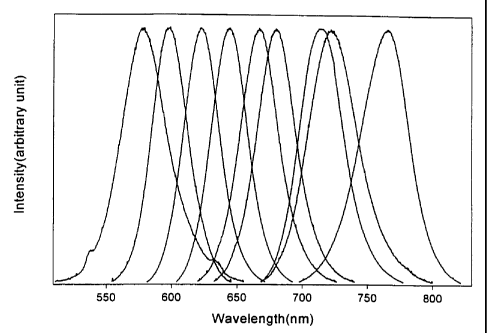
FIG. 15 shows the typical room temperature photoluminescence (PL) spectra of
CdTe nanocrystallites, which span the optical spectrum ranging from 580 nm to
770 nm.
The PL quantum efficiency of these samples range from 40% to 65% with CdTe
nanocrystallites emitting around 640 nm having the highest quantum efficiency.
The
quantum efficiency becomes lower as the size of CdTe nanocrystallites gets
smaller or
larger from the medium size. Full width half maximum (FWHM) of each spectrum
falls
in the range of 45 nm to 70 nm before the size selection procedure. After size
selection,
the FWHM of each emission spectrum drops to 35 nm. The spectra shown in FIG.
15
were obtained using CdTe nanocrystallites having diameters of 4.0 nm, 4.5 nm,
4.8 nm,
5.2nm,5.8nm,6.2nm,7.7nm,9.1 nm, 11.9nm.
A number of embodiments of the invention have been described. Nevertheless, it
will be understood that various modifications may be made without departing
from the
spirit and scope of the invention. For example, the methods and products
described
herein primarily related to CdTe nanocrystallites. However, it will be
apparent to those
skilled in the art that these methods and products can be extended to form
ZnTe, MgTe,
HgTe, and alloys of all of these tellurides. Accordingly, other embodiments
are within
the scope of the following claims.
What is claimed is:
- 17-