Note: Descriptions are shown in the official language in which they were submitted.
CA 02374397 2001-11-19
WO 00/72064 _ 1 _ PCT/US00/13833
NANOPHOTONIC DIRECTIONAL COUPLER DEVICE
FIELD OF THE INVENTION
The present invention is directed to nanophotonic devices and, more
particularly, to
nanophotonic directional coupler devices.
BACKGROUND OF INVENTION
Directional couplers transfer light signals from one waveguide to a second
waveguide,
without any direct contact of the two waveguides. The waveguides can be either
photonic wire
waveguides, such as that disclosed in U. S. Patent No. 5,878,070, or photonic
well waveguides,
such as that disclosed in U. S. Patent No. 5,790,583. U. S. Patent Nos.
5,790,583 and 5,878,070
are incorporated by reference herein in their respective entireties.
Specifically, energy is
transferred from one waveguide to the other waveguide by optical tunneling - a
process of
coherent coupling between the overlapping evanescent tails of the modes guided
in each
waveguide. Directional coupling is utilizable in wave division multiplexing
(WDM) and dense
wave division multiplexing (DWDM) applications, where light signals are
selectively
multiplexed and demultiplexed as needed.
Directional couplers are known in the prior art, such as lithium niobate
couplers.
Lithium niobate couplers, however, have a difference between the index of
refraction inside of
the waveguide and the index of refraction of the medium outside of the
waveguide that is on the
order of .01. As a result, a lithium niobate coupler must be formed to be at
least several
millimeters in length to achieve an acceptable level of signal transfer (i.e.,
transmission of the
light signal from one waveguide to the other).
Semiconductor directional couplers have also been developed in the prior art
which have
lengths on the order of several hundred microns. The decrease in length from
the lithium
CA 02374397 2001-11-19
WO 00/72064 _ 2 _ PCT/US00/13833
niobate designs is achieved due to the use of an index difference of up to .1
between the index of
refraction of a medium inside the waveguide as compared to the index of
refraction of a medium
outside of the waveguide. In particular, directional couplers are used in
connection with a
microcavity resonator, such as that described in copending U. S. Patent Appl.
Ser. No.
which consists of a oval shaped waveguide with arcuate ends, having small
circumferences (typically 5 to 20 pm), and two very small straight lengths.
The straight sections
of the oval waveguide are coupled to input and output waveguides,
respectively, via essentially
directional couplers with variable coupling factors. (The "coupling factor" is
the percentage of
power that is coupled from the input waveguide into the resonator, and is
determined by the
length of the straight section and the gap separation.) Furthermore, in
applications of resonators,
it is desirable to be able to control the polarization content of the light
that is coupled from the
waveguide into the resonator, and vice versa. Hence, a very compact and
polarization-
controllable directional coupler is an important and integral part of the
microcavity resonator
device.
Thus there exists a need in the art for an optical device that overcomes the
above-
described shortcomings of the prior art.
SUMMARY OF THE INVENTION
A nanophotonic directional coupler device is provided which has a first
waveguide and a
second waveguide. Each waveguide has a respective input port and output port
and coupling
portion disposed therebetween. The coupling portion of the first waveguide is
separated from the
coupling portion of the second waveguide.
Preferably, the directional coupler is formed within the following parameters:
a gap is
defined between the waveguides that has a width which is less than .5 ~.m; the
width of the
waveguides is less than 1 pm; the length of the coupler (referred to as
"coupler length") is less
than 50 pm; and a ratio of the index of refraction inside the waveguides to
the index of refraction
CA 02374397 2001-11-19
WO 00/72064 _ 3 _ PCT/US00/13833
of the medium (e.g. air) in the gap between the waveguides is greater than
1.5. Additionally, the
polarization of the light signal must be taken into consideration to ensure
there is the desired
level of transfer of the light signal between the waveguides.
It is preferred that symmetry be achieved in the directional coupler design.
Specifically,
the waveguides are to be identically or substantially identically formed
(materials; dimensioning)
to enable efficient transfer of the light signal. In a preferred embodiment,
the waveguides are
photonic well waveguides. On the other hand, if photonic wire waveguides are
used, the same
height in the core (the active medium through which the light propagates), in
addition to the
same width, is preferably used for both waveguides to enable efficient
transfer of the light signal.
Additionally, it is preferred that the height and width dimensions of the core
be equal.
The operation of the directional coupler is affected by the polarization of
the light signal.
For transverse electric (TE) signals, it is preferred that the width of the
waveguides be less than
.25 q.m. As for transverse magnetic (TM) signals, it is preferred that the
width of the waveguides
be greater than .35 p.m. If a directional coupler is designed to accommodate a
light signal of a
certain polarization, it will not operate efficiently with a signal of a
different polarization. For
example, if a directional coupler is designed specifically to accommodate a TE
light signal (be
less than .25 Vim), a TM signal will pass through the directional coupler with
little or no transfer
of signal.
It is possible to form the directional coupler to be polarization independent -
i.e., able to
transfer light signal of either polarization. To form a "universal"
directional coupler which is
partly insensitive to polarization, the width of the waveguides may be formed
greater than .25
qm and less than .35 Vim. However, it should be noted that this "universal"
design will not
perform as well for each polarization as if the directional coupler was
designed specifically for
each polarization as described above. Moreover, a true polarization-
independent directional
coupler can be designed for certain specific parameters wherein the device is
formed to transfer
CA 02374397 2001-11-19
WO 00/72064 - 4 - PCT/US00/13833
light with a transverse electric polarization at substantially the same power
factor as light with
transverse magnetic polarization. Although this design is limited to the
design parameters, it is
equally effective for both polarizations.
The above-described parameters affect the performance characteristics of the
directional
coupler. Theoretically, all of a light signal (100%) can transfer from one
waveguide to the other
in a directional coupler. Under actual conditions, there are losses and
perfect "complete" transfer
of signal cannot be achieved. However, the various parameters described above
can be adjusted
to obtain different degrees of signal transfer.
Accordingly, it is an object of the subject invention to provide an improved
directional
coupler for transferring a light signal between two waveguides.
An additional object of the subject invention is provide a nanophotonic
directional
coupler which can be adapted to favor a polarization or be formed
substantially polarization
independent.
The invention accordingly comprises the features of construction, combination
of
elements, and arrangement of parts which will be exemplified in the disclosure
herein, and the
scope of the invention will be indicated in the claims.
BRIEF DESCRIPTION OF THE DRAWINGS
In the drawing figures, which are not to scale, and which are merely
illustrative, and
wherein like reference numerals depict like elements throughout the several
views:
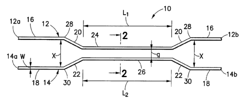
FIG. 1 is a top plan view of a directional coupler formed in accordance with
the subject
W vention;
FIG. 2 is a schematic cross-sectional view taken along line 2-2 of FIG. l;
FIG. 3 is a graph showing the relationship of coupling length and gap size at
various
waveguide widths and with both TE and TM polarizations;
CA 02374397 2001-11-19
WO 00/72064 _ 5 - PCT/US00/13833
FIG. 4 is a graph showing the relationship between the difference in
theoretical coupling
lengths for TE and TM signals at a given set of parameters and the refractive
index of the gap;
FIG. 5 is a graph showing the relationship between coupling length and gap at
various
waveguide widths for a directional coupler formed to accommodate a TM light
signal; and,
FIG. 6 is a graph showing theoretical and experimental relationships of
coupler length
and power factor for a directional coupler comprising waveguides having a
width of .4 ~m and a
gap of .2 ~,m being defined therein.
DETAILED DESCRIPTION OF THE PRESENTLY PREFERRED EMBODIMENTS
Referring to FIG. l, a nanophotonic directional coupler device 10 is generally
shown
which is defined by two waveguides: an input waveguide 12 and an output
waveguide 14. Both
waveguides 12, 14 are elongated and formed with input ports 12a, 14a,
respectively, and output
ports 12b, 14b, respectively. The waveguides 12, 14 are formed to propagate
light from one
respective port to the other.
Although not shown, the directional coupler device 10 may be formed as part of
a semi-
conductor device that can be used for light signal management, such as
multiplexing and de-
multiplexing. The directional coupler device 10 functions to transfer a light
signal from one of
the waveguides 12, 14 to the other. To illustrate the operation of the
invention, by way of non-
limiting example, it is assumed herein that a light signal is input through
the input port 12a of
the input waveguide 12 to be propagated towards the output port 12b, and
transferred to the
output waveguide 14. Once the light signal is transferred, it will continue to
propagate in the
same direction as prior to transfer. Thus, in the given example, a transferred
light signal will
propagate towards the output port 14b of the output waveguide 14. As is
readily appreciated,
light signals can enter and exit the directional coupler device 10 in various
directions, and the
terms "input" and "output" are used for convenience.
CA 02374397 2001-11-19
WO 00/72064 _ 6 _ PCT/US00/13833
The waveguides 12, 14 are each formed with transmitting portions 16, 18,
respectively,
transition portions 20, 22, respectively, and coupling portions 24, 26,
respectively. For each of
the waveguides 12, 14, the various portions extend continuously to form a
unitary waveguide
structure.
The coupling portions 24, 26 are disposed to define a gap therebetween having
a width g,
which is discussed further below. It is preferred that the coupling portions
24, 26 be both
substantially straight and that the portions 24, 26 be substantially parallel.
Also, the coupling
portions 24, 26 have coupler lengths L1, L2, respectively. It is preferred
that the coupling lengths
L 1, L2 be equal.
The transmitting portions 16, 18 are wholly at least spaced apart a distance
x, which is
greater than the width of the gap g. The transmitting portions 16, 18 carry
light signals to and
from the directional coupler device 10 and may be formed with various lengths.
Additionally, the
transmitting portions 16, 18 need not be straight. The key aspect of the
transmitting portions 16,
18 is that they be spaced apart a greater distance than the coupling portions
24, 26.
The transition portions 20, 22 extend between and connect the coupling
portions 24, 26
with the transmitting portions 16, 18. Specifically, the transition portions
20, 22 extend away
from the coupling portions 24, 26 to have respective ends 28, 30 spaced apart
by the distance x.
By way of non-limiting example, the transition portions 20, 22 and the
transmitting portions 16,
18 may be formed straight, with the transmitting portions 16, 18 of the
waveguides 12, 14 being
parallel. Also, for each of the waveguides 12, 14, the transmitting portions
16, 18 may be
collinearly aligned.
The directional coupler device 10 may be formed with various combinations of
dimensions. The following is a list of critical parameters for the directional
coupler device 10
and their acceptable values.
CA 02374397 2001-11-19
WO 00/72064 _ ~ _ PCTNS00/13833
GAP WIDTH (~)
It is preferred that the gap width g between the coupling portions 24, 26 be
less than .5
Vim. The gap width g required for a specific application is calculated as
follows:
g = 2 - z , Eq. 1
where,
~, is the wavelength of the light signal in free space;
nwg is the index of refraction inside the waveguide; and,
ng is the index of refraction of a medium disposed in the gap.
The light signal that is propagated through the waveguides 12, 14 will often
cover a range of
wavelengths. In particular, the light signal is generated by a lasing device
that pumps the signal
at a desired wavelength (typically 1550 nm) or over a range of wavelengths.
Referring to FIG. 2, each waveguide 12, 14 includes a core 11 preferably
disposed
between cladding layers 13. The index of refraction inside the waveguide nwg
is the index of
refraction of core 11 of the waveguides. The core 11 is the active medium
through which the
light signal actually propagates. The core 11 may be surrounded by cladding
layers 13 and/or
substrate 15 and may be formed from Gallium Arsenide or Indium Phosphide; both
these
materials have an index of refraction that is approximately 3.5. Moreover, it
is preferred that
deep etching be used to form the waveguides 12, 14. Additionally, the index of
refraction ng
refers to the index of refraction of a medium that is disposed in the gap g.
Most typically, the
medium will be air, having an index of refraction of 1Ø However, other
insulative mediums can
be used.
CA 02374397 2001-11-19
WO 00/72064 _ g _ PCT/US00/13833
WAVEGUIDE WIDTH (w)
The waveguides 12, 14 are each formed with a width w that is preferably less
than 1 Vim.
The specific width w is calculated by the following equation,
w = ~,/ nwg Eq. 2.
Preferably, the two waveguides 12, 14 have the same width w. Additionally, if
the waveguides
12, 14 are photonic wire waveguides, then the height h of the core 11 (as
shown in FIG. 2) is
also preferably made equal between the two waveguides 12, 14. It is also
preferred that for
photonic wire waveguides, the width w be equal to the height h.
COUPLER LENGTH (L 1, L2)
As discussed above, the coupler portions 24, 26 of the waveguides 12, 14 are
each
formed with a respective coupler length L1, L2. Preferably, the coupler
lengths L1, L2 are made
equal. Additionally, in a preferred embodiment, the coupler lengths L1, L2 are
to be less than 50
Vim.
RATIO OF INDICES OF REFRACTION
The ratio of the index of refraction inside the waveguide nwg to the index of
refraction of
the medium inside the gap ng is preferably greater than 1.5. Stated simply,
nwg/ng > 1.5 Eq. 3.
The large difference in the indices of refraction provides strong confinement
of a light signal
inside the respective waveguides 12, 14 and provides for a more efficient
light signal transfer
between the waveguides 12, 14 than that found in the prior art.
POWER FACTOR
CA 02374397 2001-11-19
WO 00/72064 _ 9 _ PCT/US00/13833
The power factor is the indicator of the performance of the directional
coupler device 10.
The parameters discussed herein have an impact on the power factor. With
directional couplers,
the term "power factor" is used to indicate what percentage of a signal,
assuming no losses, will
transfer in a directional coupler. Thus, by varying one or more parameters, a
desired power factor
can be obtained. Specifically, power factor is calculated by finding a
theoretical coupling length
(Lc) for a specific design at which 100% of the light signal theoretically
passes from one
waveguide to the other, assuming no losses. The theoretical coupling length
may be calculated as
follows:
L . = Eq. 4.
where,
Ns is an effective index of refraction for the symmetric mode of the coupled
waveguides; and,
NA is an effective index of refraction for the asymmetric mode of the coupled
waveguides.
To achieve a theoretical complete transfer in the directional coupling device
10, the
theoretical coupling length Lc is solved for, and the coupler lengths L1, L2
are set equal thereto.
The power factor (Fc) can be calculated as follows,
F'. = sine [~cL l (2L~)] , Eq. 5.
where,
L is the actual coupler length for which the power factor is being calculated.
Thus, the power factor is a function of the actual coupler length and the
theoretical coupling
length. Theoretically, the power factor equals 1.0 where L = Lc - however, a
power factor of 1.0
cannot be actually achieved because of losses. It should also be noted that
the power factor can
be less than one, both at lengths greater than and less than the theoretical
coupling length.
CA 02374397 2001-11-19
WO 00/72064 _ 1 ~ _ PCT/US00/13833
POLARIZATION
As discussed above, light signals have either a TM polarization or a TE
polarization. As
a result, signals of different polarizations behave differently and have
different transfer
characteristics when used with a directional coupler. For example, the
effective indices of
refraction NS and NA are respectively generally different for TE and TM
signals. To take
polarization into consideration, a TM specific directional coupler is
preferably designed with the
additional limitation that the waveguide width w is greater than .35 pm. In
contrast, a TE
specific directional coupler is preferably designed with the additional
limitation that the
waveguide width w is less than .25 p.m. It should be noted that a light signal
with a TM
polarization will not transfer in a TE specific directional coupler, whereas,
a light signal with a
TE polarization may partially transfer in a TM specific directional coupler.
In either case, there is
very inefficient or no transfer of signal. Furthermore, the TM specific
directional couplers
generally have larger coupling lengths that TE specific directional couplers.
This means that in
order to design a directional coupler that favors a particular polarization,
the directional coupler
must satisfy a certain combination of waveguide width, gap size and length
simultaneously.
However, under certain limited circumstances, polarization dependency can be
limited or
even eliminated. Operationally, a polarization independent directional coupler
is one in which
both TE and TM polarized lights will transfer equally from one waveguide to
the other. In other
words, the coupling length for the TE signal (LcTE) is equal to the coupling
length for the TM
signal (LcTM). Therefore OLc, which is equal to LcTE _ LcTM is equal to zero
for a polarization
independent waveguide.
Referring to FIG. 3, two families of curves representing both TE and TM values
for
different waveguide widths w are plotted as a function of gap size (g). FIG. 3
was prepared with
ng = 1Ø A shaded band S represents the range of waveguide widths w of .25
p.m to .35 ~,m. In
CA 02374397 2001-11-19
WO 00/72064 - 1 1 _ PCT/US00/13833
this range of w, the coupler lengths are approximately the same for both TE
and TM light
polarized signals for all gap sizes. In particular, FIG. 3 shows that TE and
TM curves for w =
0.3 pm cross at a point where the gap size is approximately 0.2 p.m. This
means that a
directional coupler design with the parameters w = 0.3 p,m and g = 0.2 ~m will
be polarization
independent.
For true polarization independence the theoretical coupling length for a TE
signal (LcTE)
and the theoretical coupling length for a TM signal (LcTM) will be equal for a
given set of
parameters. Thus, OLc, which is equal to LcTE _ LcTM~ is equal to zero for a
polarization-
independent design.
As an illustrative example, set forth below is Table 1 that includes
calculations of OLc
for various indices of refraction inside the gap ng
TABLE 1
llg Ns NA Lc (Nm) Ns Nn Lc (Nm) OLc (N~m)
(TE) (TE) (TE) (TM) (TM) (TM)
1.8 2.8504762.82424529.545 3.0105442.98356228.723 0.822
1.82 2.8542332.82738928.871 3.0116012.98429828.385 0.486
1.84 2.8580202.83055728.220 3.0126792.98504628.046 0.174
1.85 2.8599272.83214827.899 3.0132282.98542427.874 0.025
1.86 2.8618402.83374727.587 3.0137812.98580527.702 -0.115
1.88 2.8656982.83696326.971 3.0149052.98658827.369 -0.398
1.9 2.8695852.84020626.379 3.0160562.98738027.026 -0.647
CA 02374397 2001-11-19
WO 00/72064 _ 12 _ PCT/US00/13833
Table 1 was prepared with the following parameters: gap width g = .25 Vim;
waveguide width w
_ .4 Vim; optical wavelength ~,= 1.55 pm; and the index of refraction inside
the waveguide nwg =
3.4.
As shown in Table 1, the values for OLc switch from positive values to
negative values
between the ng values 1.85 and 1.86. Specifically, it has been calculated that
OLc equals zero at
ng = 1.8516. Thus, true polarization independence is achieved at that point,
and Table 2 sets
forth the values associated with the point:
TABLE 2
llg Ns NA Lc (gym)Ns Na Lc (Nm) OLc (gym)
(TE) (TE) (TE) (TM) (TM) (TM)
1.8516 2.8602332.832403 27.8476 3.0133162.985486 27.8476 0.0000
Additionally, FIG. 4 is a graph plotting OLD versus the refractive index of
the gap ng. For ng =
1.8516, OLD equals zero.
As those skilled in the art will recognize, the example set forth above is for
illustration,
and other points of polarization independence can be achieved by varying the
parameters,
calculating NA and Ns for the parameters for both TE and TM signals, and
determining ~L~. The
four primary parameters that effect polarization independence are: the
refractive index inside the
gap n g; the refractive index inside the waveguide nwg; the gap width g; and
the waveguide width
w. By way of example, Table 3 indicates a second point of polarization
independence for
different parameters (unless indicated otherwise the same parameters apply as
indicated with
respect to Table 1 ).
TABLE 3
CA 02374397 2001-11-19
WO 00/72064 - 13 - PCT/US00/13833
ng Gap Width Waveguide widthLo (gym) Lo (gym) OLD (gym)
(g) (TE) (TM)
1.65 0.6 0.45 1655.986 1655.986 0.00
With the foregoing information, the directional coupler device 10 may be
designed with
numerous dimensional combinations and performance characteristics, even those
outside of the
range of the preferred embodiment. By way of non-limiting example, reference
is made to FIG.
5, which shows gap width g being plotted versus theoretical coupling length
(Lc) for a
waveguide having a width w of .4 Vim. The plot assumes ~,=1.55 ~.m, and the
ratio of the indices
of refraction nwg, ng to be greater than 1.5. As indicated on the plot, a TM
polarization is also
assumed.
To verify the accuracy of the theoretical coupling length, and determine
actual losses, a
directional coupler was built with waveguide width w of .4 pm and a gap of .2
pm.
Additionally, the directional coupler was built with ~, = 1.55, ng = 1.5, and
nwg = 3.4. The
coupling length was varied and the intensity of the output signal from both
the input waveguide
and the output waveguide were measured. The measured intensity of the signal
outputted from
the output waveguide was divided by the intensity of the input signal to
calculate the actual
power fraction. Referring to FIG. 6, the experimental points indicate test
points of the actual
power fraction versus the length of the coupler used at that point (actual
physical length of
directional coupler). The plot of FIG. 6 also includes a curve indicating the
theoretical power
fraction values over the disclosed range of coupler lengths. As will be noted,
the experimental
values track the theoretical values fairly well. Note that theoretically the
coupling length is the
length where the maximum power fraction occurs.
CA 02374397 2001-11-19
WO 00/72064 - 14 - PCT/US00/13833
Referring to FIG. 5, the theoretical coupling length for a gap g of
approximately .2 ~.m is
approximately 25 pm. Experimentally the maximum power fraction (0.9) occurs at
the coupler
length of 25 ~,m, which agrees with the theoretical coupler length. As shown
in FIG. 6, with an
actual coupling length of 25 Vim, the actual power fraction is approximately
.9 and located at the
highest point of the plotted experimental points. Therefore, an actual
coupling length of 25 ~m
for the given parameters provides a substantially complete transfer of energy,
wherein a much
higher rate of signal transfer is achieved than with other coupling lengths.
Accordingly, with the
parameters disclosed herein, a directional coupler can be formed having a
length less than 50 ~m
which is capable of achieving substantially complete signal transfer - the
range of coupling
lengths of the subject invention are much lower than that found in the prior
art and defines a
substantial improvement thereover.
Thus, while there have been shown and described and pointed out fundamental
novel
features of the invention as applied to preferred embodiments thereof, it will
be understood that
various omissions and substitutions and changes in the form and details of the
disclosed
invention may be made by those skilled in the art without departing from the
spirit of the
invention. It is the intention, therefore, to be limited only as indicated by
the scope of the claims
appended hereto.
It is also to be understood that the following claims are intended to cover
all of the
generic and specific features of the invention herein described and all
statements of the scope of
the invention which, as a matter of language, might be said to fall
therebetween.