Note: Descriptions are shown in the official language in which they were submitted.
CA 02374401 2001-11-19
WO 00/72065 _ 1 _ PCT/US00/13856
OVAL RESONATOR DEVICE
FIELD OF THE INVENTION
This invention relates to nanophotonic devices, and, more particularly, to
optical
resonator devices.
BACKGROUND OF INVENTION
Optical elliptical resonators, including circular resonators, are known in the
prior art. For
example, U. S. Patent No. 5,926,496 entitled "SEMICONDUCTOR MICRO-RESONATOR
DEVICE" which issued on July 20, 1999 to the inventors herein, discloses a
micro-resonator
device having a circular disk shape, an annular ring shape, or a distorted
disk shape or ring that
partially follows the outline of a circular diameter. Although this device is
very effective in
causing light transference of a light signal on resonance with the resonator,
the use of an
elliptical resonator causes phase mismatch with the light travelling in an
adjoining input/output
waveguide. In particular, reference is made to FIG. 1, which was taken from
FIG. 8 of U. S.
Patent No. 5,926,496. As shown therein, light propagating in the waveguide
1050 that is on
resonance with the resonator 1052 is coupled over an optical path length Os2
of the waveguide
1050 with an optical path length Osi of the resonator 1052. Over the arc angle
0, the coupled
light may go out of phase due to the difference in optical path length (~s2 -
Os~). U. S. Patent
No. 5,926,496 is concerned with limiting the phase mismatch to less than ~/2.
To achieve this
objective, it is indicated that the coupling length should not exceed
approximately 1/lOt~' the
resonator circumference. As is readily appreciated, the same phase mismatch
problem is present
in non-circular, elliptical resonator devices, and where straight waveguides
are in an elliptical
resonator device.
CA 02374401 2001-11-19
WO 00/72065 _ 2 _ PCT/US00/13856
Additionally, the gap size (the distance between the resonator and the
input/output
waveguide) is generally very small with elliptical resonator devices. The
small size ensures that
acceptable coupling efficiency (the percentage of optical power coupled from
the input to the
resonator and from the resonator to the output) is achieved. For example, as
shown in FIG. 1 A,
which was taken from U. S. Patent No. 5,926,496, an exemplary gap width gw of
.1 ~m is
disclosed between the resonator 1052 and the straight waveguide 1050B with an
effective
coupling length of 1.0 pm. The coupling length is relatively short due to the
short interaction
distance between the resonator and the coupled straight waveguide. As is
readily appreciated,
the interaction distance is kept to a minimum with a circular resonator being
used.
Thus, there exists a need in the art for an optical device that overcomes the
above-
described shortcomings of the prior art.
SUMMARY OF THE INVENTION
The aforementioned objects are met by an optical resonator device which
includes an
oval resonator, an input waveguide, and an output waveguide. The oval
resonator operates to
transfer signals from the input waveguide to the output waveguide. As used
herein, the term
"oval" refers to a continuous form having two arcuate ends and two straight
sides extending
therebetween. It is preferred that the straight sides of the oval resonator be
generally parallel.
The input waveguide and the output waveguide, each respectively have an input
port, an
output port, and portions that are respectively spaced from the straight sides
of the oval resonator
to define gaps therebetween. As described below the device is usable in
various applications.
The oval shape of the resonator of the subject invention overcomes the phase
mismatch
problem found in the prior art. In particular the input and output waveguides
preferably have
portions thereof aligned substantially parallel to the straight sides of the
resonator so as to define
elongated, constant-width input and output gaps between the waveguides and the
resonator. The
CA 02374401 2001-11-19
WO 00/72065 _ 3 _ PCT/US00/13856
elongation and constant width of the respective gaps define longer coupling
lengths across which
signals may couple. (The coupling length is the length of optical path along
which coupling
occurs.) In prior art elliptical resonator devices, such as the circular
resonator device discussed
above, the coupling length is difficult to determine due to the differences in
optical path lengths.
With the straight sides of the oval resonator, the same length optical paths
are defined in the
input and the output waveguides as in the resonator. As a result, not only is
the coupling length
more clearly defined, but also the efficacy of the resonator device is
increased.
The oval resonator device preferably is formed within the following
dimensional
parameters: gaps between the resonator and the input waveguide and the output
waveguide,
respectively, have a width of less than .5 pm; a width of less than 1.0 ~.m is
preferably defined in
the resonator, the input waveguide, and the output waveguide; coupling lengths
of less than 10.0
~m are preferably utilized; and, the ratio of the index of refraction of the
core of the waveguides
and the oval resonator to the index of refraction of a medium in the gaps is
preferably greater
than 1.5.
With the specified parameters, the oval resonator device preferably operates
at a coupling
factor of approximately 0.01 - 0.1. The coupling factor is a decimal
representation of the
percentage of optical power of a signal that is transferred between the
resonator and the adjacent
waveguides. The portion of the signal in the input waveguide whose wavelength
is on resonance
with the resonator passes through the resonator to the output waveguide,
whereas portions of the
signal in the input waveguide which are off resonance with the resonator by-
pass the resonator
and exit from the input waveguide. Thus, the oval resonator serves as a
wavelength filter that
separates out the resonance wavelengths from the remainder of the signal. The
resonance
condition is satisfied when the round-trip length of the resonator is equal to
an integer multiple
of the optical wavelength in the waveguide medium.
CA 02374401 2001-11-19
WO 00/72065 _ 4 _ PCT/US00/13856
The coupling factor is dependent on several factors including the gap widths,
the
coupling lengths, the waveguide widths, the indices of refraction, the
polarization of the light
being transferred, and the wavelength of the light. With the subject
invention, the gap widths
can be made larger than that disclosed in the prior art circular resonator
device, with longer
coupling lengths being used to achieve the same coupling factor as the
circular resonator device.
The increase in gap widths causes a drop in coupling factor, wherein, an
increase in coupling
length causes an increase in coupling factor. With the subject invention, by
increasing the
coupling length, an increase in coupling factor is achieved that is at least
commensurate with the
drop in the coupling factor caused by the increase in the gap width. The net
effect is to produce
a resonator device that is easier to manufacture, because of the more generous
gap width than
that in the prior art, without any sacrifice in performance. Additionally, the
coupling lengths can
be easily changed in the resonator device, since the length of the side
portions can be increased
as needed to achieve the desired coupling factor, without requiring the
arcuate ends to be altered.
In this manner, oval resonators with generally the same overall width (as
measured between the
straight portions) can operate with different coupling factors. In contrast,
the elliptical resonators
of the prior art, including circular resonators, require changes in curvature,
gap widths, etc., to
achieve changes in coupling factor - which is difficult to realize.
The oval resonator is preferably defined by a single, uninterrupted waveguide
element
that is formed to define the oval shape. It is preferred that symmetry be
achieved in the oval
resonator device. Specifically, the input waveguide, the output waveguide, and
the waveguide
element of the resonator are preferably identically or substantially
identically formed (materials;
dimensioning) to enable efficient transfer of the light signal. The waveguides
and waveguide
element can be either photonic wire waveguides, such as that disclosed in U.
S. Patent No.
5,878,070, or photonic well waveguides, such as that disclosed in U. S. Patent
No. 5,790,583. It
is preferred that photonic well waveguides be used with the subject invention.
If photonic wire
CA 02374401 2001-11-19
WO 00/72065 _ 5 _ PCT/US00/13856
waveguides are used, the same height in the core of the waveguides and the
waveguide elements,
in addition to the same width, is preferably used to enable efficient transfer
of the light signal.
Additionally, it is preferred that the height and width dimensions of the core
be equal. U. S.
Patent Nos. 5,790,583 and 5,878,070 are incorporated by reference herein in
their respective
entireties.
The oval resonator device can be used to form various devices, including, but
not limited
to, channel-dropping filters, switches, tunable filters, phase modulators, and
1 x N
multiplexers/demultiplexers. Additionally, multiple oval resonators can be
arranged in an array,
either in parallel or in series, to manipulate the frequency spectrum of the
output signal.
The invention accordingly comprises the features of construction, combination
of
elements, and arrangement of parts which will be exemplified in the disclosure
herein, and the
scope of the invention will be indicated in the claims.
BRIEF DESCRIPTION OF THE DRAWINGS
In the drawing figures, which are not to scale, and which are merely
illustrative, and
wherein like reference numerals depict like elements throughout the several
views:
FIG. 1 is a top plan view of a prior art circular resonator device;
FIG. 1 A is a top plan view of a prior art circular resonator device with a
straight
waveguide;
FIG. 2 is a top plan view of an oval resonator device formed in accordance
with the
subject invention;
FIG. 3 is a partial cross-sectional view taken along line 3-3 of FIG. 2;
FIG.4 is a top plan view of a channel-dropping filter device formed in
accordance with
the subject invention;
FIG. 5 is a graph indicating the output of the input waveguide (reflection) of
the channel-
dropping filter device shown in FIG. 4;
CA 02374401 2001-11-19
WO 00/72065 _ 6 _ PCT/US00/13856
FIG. 6 is a graph indicating the output of the output waveguide (transmission)
of the
channel-dropping filter device shown in FIG. 4;
FIG. 7 is a top plan view of a 1 x 4 multiplexer/demultiplexer device formed
in
accordance with the subject invention;
FIG. 8 is a top plan view of a device having a cascaded array of oval
resonators arranged
in parallel;
FIG. 9 is a top plan view of a device having a cascaded array of oval
resonators arranged
in series; and,
FIG. 10 is a top plan of a phase modulator device formed in accordance with
the subject
invention.
DETAILED DESCRIPTION OF THE PREFERRED EMBODIMENTS
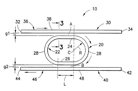
Referring to FIG. 2, an oval resonator device is depicted and generally
designated with
the reference numeral 10. The device 10 includes an oval resonator 20, an
input waveguide 30,
and an output waveguide 40.
The oval resonator 20 is preferably defined by a single, uninterrupted
waveguide element
22. The element 22 has two generally straight portions: a first straight
portion 24 and a second
straight portion 26. Also, two arcuate ends 28 extend between and connect the
straight portions
24 and 26. It is preferred that the oval resonator 20 have a symmetrical
appearance with the
straight portions 24 and 26 being substantially parallel and having generally
the same length L.
Also, the arcuate ends 28 are preferably formed with the same degree of
curvature. For example,
the arcuate ends 28 may respectively be each defined about a center C and
formed by a radius R.
The center C is preferably aligned with ends of the straight portions 24, 26
such that the arcuate
ends 28 are each semi-circular in shape.
CA 02374401 2001-11-19
WO 00/72065 _ ~ _ PCT/US00/13856
The input waveguide 30 has an input port 32, an output port 34, and a signal
transmitting
portion 36 extending therebetween. A length 38 of the signal transmitting
portion 36 is located
in proximity to the first straight portion 24 so as to define a gap A
therebetween having a width
g1. It is preferred that the length 38 be substantially parallel to the
straight portion 24, so as to
define a substantially constant gap width g1 along the complete length L of
the first straight
portion 24.
The output waveguide 40 has an input port 42, an output port 44, and a signal
transmitting portion 46 extending therebetween. A length 48 of the signal
transmitting portion
46 is located in proximity to the second straight portion 26 so as to define a
gap B therebetween
having a width g2. It is preferred that the length 48 be substantially
parallel to the second straight
portion 26, so as to define a substantially constant gap width g2 along the
complete length of the
second straight portion 26. It is also preferred that the width g1 be equal to
the width g2.
With the oval resonator 20 being tuned to a predetermined resonance frequency,
a
portion of a signal travelling from the input port 32 towards the output port
34 of the input
waveguide 30 that is on resonance with the oval resonator 20, interferes
constructively, resonates
and passes through the oval 20 resonator to the output waveguide 40, whereas
portions of the
signal that are off resonance with the oval resonator 20 continue to the
output port 34 and are
emitted as a reflection signal. The resonated signal passes to the output
waveguide 40. Because
of the shape of the oval resonator 20, the resonated signal will pass into the
output waveguide 40
in an opposite direction from the signal travelling in the input waveguide 30,
as indicated by the
arrows. Specifically, the resonated signal will pass into the output waveguide
40 travelling in a
direction towards the output port 44 and be emitted therefrom as a
transmission signal. To direct
the resonated signal in the output waveguide 40 in the same direction as the
input waveguide 20,
the output waveguide 40 can be curved as shown in FIG. 4, to have an arcuate
bend 50,
preferably of 180°. It is to be understood that the references to
"input" and "output" herein are
CA 02374401 2001-11-19
WO 00/72065 _ g _ PCT/US00/13856
only for convenience; the oval resonator device 10 can be used with a signal
passing through the
waveguides in any direction consistent with the disclosure herein.
It is preferred that symmetry be achieved in the oval resonator device 10.
Specifically,
the input waveguide 20, the output waveguide 30, and the waveguide element 22
of the oval
resonator 20 are preferably identically or substantially identically formed
(materials;
dimensioning) to enable efficient transfer of the light signal. The waveguides
20, 30 and the
waveguide element 22 can be either photonic wire waveguides or photonic well
waveguides that
extend from a substrate 52. Etching techniques knovm in the prior art can be
used to form the
waveguides 20, 30 and the waveguide element 22. It is preferred that photonic
well waveguides
be used with the subject invention.
FIG. 3 depicts a representative cross-section of the input waveguide 30, along
with the
waveguide element 22. The output waveguide 40 preferably has the same cross-
section that is
shown. As shown representatively, a core 54 is provided surrounded by layers
of cladding 56.
The core 54 is the active light carrying medium, and the core 54 of each of
the respective
waveguides 30, 40 and the waveguide element 22 is preferably formed with a
width w. If
photonic wire waveguides are used, the same height h is preferably used with
each of the cores
54, in addition to the same width w, to enable efficient transfer of the light
signal. Additionally,
it is preferred that the height h and width w dimensions of the cores 54 be
equal.
FIGS. 5 and 6 depict performance characteristics of the oval resonator device
10 as
shown in FIG. 4. FIG. 5 is a graph that shows the intensity of the reflection
signal emitted from
the output port 34 of the input waveguide 30, whereas, FIG. 6 shows the
intensity of the
transmission signal emitted from the output port 44 of the output waveguide
40. The lowest
values on the graph in FIG. 5 correspond to approximately 1522.5 nm and 1542.5
nm
wavelengths, respectively. As a corollary, the highest values on the graph in
FIG. 6 also
correspond to 1522.5 nm and 1542.5 nm, respectively. The graphs represent a
spectrum
CA 02374401 2001-11-19
WO 00/72065 _ 9 _ PCT/US00/13856
resonating about 1542.5 nm with portions of the signal at this wavelength
being passed from the
input waveguide 30 to the output waveguide 40. The portions of the signal that
do not resonate
by-pass the oval resonator 20 and are emitted from the output port 34 of the
input waveguide 30
as the transmission signal. The wavelength at which the oval resonator 20 is
set to resonate is
adjustable using techniques known to those skilled in the art, such as by
applying different
electric voltages to the resonator.
DESIGN PARAMETERS
It is preferred that the oval resonator device 10 be formed within the ranges
of certain
parameters. First, it is preferred that the widths g1 and g2 be less than .5
Vim. More specifically,
it is preferred that the widths g1 and g2 be selected so as to conform with
the following
relationship,
gap width (g1 or g2) <- 2 2 , Eq. (1)
nW6 - n~
where,
7~ is the wavelength of the signal in vacuum;
nwg is the index of refraction inside the core of the waveguide; and,
ng is the index of refraction of a medium disposed in the respective gap.
Second, it is preferred that the waveguides 30; 40 and the waveguide element
22 be each
formed with a width w that is less than .5 ~.m. The preferred width w enables
the waveguides
30, 40 and the waveguide element 22 to fulfill a single-mode requirement
(i.e., the respective
waveguide/waveguide element supports only one fundamental transverse electric
(TE) and one
fundamental transverse magnetic (TM) mode.
CA 02374401 2001-11-19
WO 00/72065 _ 1 p _ PCT/tTS00/13856
Third, it is preferred that the length L of both the straight portions 24 and
26 be less than
Vim. The length L is limited by the round-trip length of the oval resonator
20, as described
below.
Fourth, it is preferred that the ratio of the index of refraction inside the
core of the
waveguide nwg to the index of refraction of the medium inside the respective
gap ng be greater
than 1.5. Stated algebraically,
nwg/ng> 1.5. Eq. (2)
Fifth, round-trip loss must be taken into consideration. With the specified
parameters,
the oval resonator device 10 preferably operates at a coupling factor of
approximately 0.01 - 0.1.
The coupling factor is a function of the gap widths (g1, g2), the coupling
length (L), the indices
of refraction (nwg, ng), the polarization of the light being transferred, and
the wavelengths of the
light (~,). Within the preferred ranges, the gap widths g1, g2 can be made
larger than that
disclosed with the elliptical and circular resonator devices of the prior art.
To compensate for
loss in coupling factor due to increases in the gap widths, the coupling
lengths L are increased so
as to achieve at least the same coupling factor as the circular resonator
device.
The oval resonator device 10, as with all closed loop devices, is susceptible
to "round trip
loss" with a certain portion of the signal being lost upon traversing the oval
resonator 20. It is
preferred that the coupling factor of the oval resonator device 10 be greater
than the round trip
loss, and more preferably, several times greater than the round trip loss. In
an exemplary
embodiment, with a round trip loss of 0.03 (i.e., 3%), the coupling factor may
be 0.13 (i.e.,
13%), i.e., more than four times greater than the round trip loss. In this
manner, the detrimental
effects of round trip loss can be kept to a minimum. Admittedly, a coupling
factor of 0.13
exceeds the preferred range of 0.01 - 0.1. The range of 0.01 - 0.1 is more
applicable where
minimal round trip losses are present.
CA 02374401 2001-11-19
WO 00/72065 _ 1 1 _ PCT/US00/13856
A sixth design parameter which needs to be considered in the design of the
oval
resonator device 10 is the resonance wavelengths and free spectral range
(FSR). Resonance
wavelengths occur periodically with uniform spacing therebetween. The
resonance wavelengths
(~,m) are given by
m7~", = rleffL~ E~l~ (3)
where m is an integer.
The term "m" is known as the order of the resonance, "new" is the effective
refractive
index of the resonator, and "neffL" is the optical length of the resonator.
The spacing between
successive resonances is known as the free spectral range (FSR). Hence, it can
be seen that the
smaller the resonator is, the larger the FSR will be.
Advantageously, the oval resonator device 10 can be used in various devices
and
configurations. The resonance wavelength of the resonator, being determined by
the optical
length of the resonator, can be tuned or modulated by modulating the effective
index of the
resonator. This can be achieved using the electro-optic effect in the
semiconductor material
comprising the waveguide, whereby an electric field (or voltage) is applied
directly to the
resonator to modify the refractive index of the material therein. For example,
FIG. 4 depicts a
channel-dropping filter or a wavelength switch. As a channel-dropping filter,
the device simply
drops a particular wavelength (or channel) from the input signal that
corresponds to the
resonance wavelength of the resonator. As a wavelength switch, the device is
operated as a
tunable filter that is being tuned between being on and being off resonance
for the particular
wavelength to be switched.
Additionally, the device 10 can be used in a 1 x N multiplexer/demultiplexer
device,
such as the 1 x 4 multiplexer/demultiplexer device 100 shown in FIG. 7.
Herein, four oval
resonators 120A, 120B, 120C, and 120D are arranged along a common input
waveguide 130,
although any number of the oval resonators may be used in conjunction with the
device. The
CA 02374401 2001-11-19
WO 00/72065 _ 12 _ PCT/US00/13856
oval resonators 120A-D are each tuned to resonate at a different wavelength so
that different
portions of the signal travelling through the input waveguide 130 are caused
to be resonated by
the various oval resonators 120A-120D and passed along to the respective
output waveguides
140A-D, thereby demultiplexing the signal. The device 100 can also be used in
"reverse" to
multiplex signals travelling through the output waveguides 140A-D and cause a
composite
signal to be generated in the input waveguide 130.
Furthermore, the device 10 can be used in a cascaded array, such as the arrays
shown in
FIGS. 8 and 9 to obtain a desired frequency spectrum. In many applications it
is desired that the
spectral characteristics of the filter exhibit a flat top shape at the peak of
a response, so as to
accommodate drift in the wavelength of the source caused by temperature or
source wavelength
fluctuations, such as shown in FIG. 6. One realization of this desired result
is depicted in FIG. 8
by a parallel array of identical resonators coupled to each other. A filter
with arbitrary
characteristics can be realized by judiciously choosing the coupling
coefficients between
individual resonators and between the resonators and the parallel straight
waveguides. In the
simplest case, one may assume these coupling coefficients to be identical. In
this case, the
overall behavior of the filter is such that the resonance wavelengths of the
individual resonators
become split into a multitude of resonances equal to the number of resonators.
The spacing
between the resonances is determined by the strength of the coupling
coefficient between the
resonators (the stronger the coupling, the larger the separation between these
resonances).
Therefore, by judiciously choosing the coupling coefficient, one can
advantageously shift the
resonances close enough so that they essentially merge together to form a
single resonance with
a flat top.
FIG. 8 specifically depicts a parallel array 200 which includes a plurality of
oval
resonators 220A, 220B, and 220C coupled to one another between input waveguide
230 and
output waveguide 240. Three oval resonators 220A-C are shown in FIG. 8 by way
of non-
CA 02374401 2001-11-19
WO 00/72065 _ 13 _ PCT/US00/13856
limiting example, and any number of resonators can be used. The oval resonator
220A is
coupled to the input waveguide 230 and to the oval resonator 220B, whereas,
the oval resonator
220C is coupled to the output waveguide 240 and to the oval resonator 220B. As
such, this
arrangement results in a frequency response in the output signal transmitted
to the output
waveguide 240 that is centered about a single resonance wavelength.
Another desirable characteristic of a filter response is that the roll-off on
the sides of the
response be sufficiently rapid so as to minimize the crosstalk between one
channel and all the
other channels (as depicted in FIG. 6). A single resonator is effectively a
first-order Fabry-Perot
filter with a Lorentzian response that has a relatively slow roll-off. To
improve the roll-off, one
can essentially cascade multiple identical resonators in series so as to
realize a higher-order filter
that by definition has a faster roll-off. This realization is depicted in FIG.
9. It is essential that
the resonators be lined up exactly in their resonance frequencies, otherwise
the output signal will
have a broader frequency spectrum. FIG. 9 depicts a series array 300 which
includes a plurality
of oval resonators 320A, 320B and 320C which are each coupled to an input
waveguide 330 and
an output waveguide 340, but not coupled to each other. Again, any number of
the oval
resonators can be used. As a result, an output signal is generated in the
output waveguide 340
that has a broader frequency spectrum with "steeper" side slope
characteristics than that
generated by a single oval resonator formed in accordance with the subject
invention.
As yet a further application, the oval resonator of the subject invention can
be used with a
single waveguide as shown in FIG. 10. Here, an all-pass filter 400 is shown,
which may be used
as a phase modulator. The all-pass filter 400 includes an oval resonator 410
disposed adjacent to
an input waveguide 420. The oval resonator 410 "reflects" light of all
frequencies passing
through the input waveguide 420 with a phase response that depends on the
coupling strength
between the oval resonator 410 and the input waveguide 420. Thus, light
passing through such a
filter undergoes no change in amplitude but a change in phase. This phase
shift can be
CA 02374401 2001-11-19
WO 00/72065 _ 14 _ PCT/US00/13856
modulated, again using the electro-optic effect applied to the resonator. This
phase modulator
can be incorporated into a Mach-Zehnder interferometer to realize amplitude
modulation. The
advantage of this phase modulator is that the required modulation voltage for
a given phase shift
(say, ~) can be very small because the resonant effect of the resonator
effectively increases the
optical length of the device. Alternatively, for a given modulation voltage,
the phase modulator
can be much smaller and yet is capable of achieving a ~-phase shift. By
applying and varying a
voltage to the oval resonator 410, the phase of the light can be altered. The
all-pass filter 400 of
the subject invention is considerably smaller than phase modulators formed in
the prior art.
Thus, while there have been shown and described and pointed out fundamental
novel
features of the invention as applied to preferred embodiments thereof, it will
be understood that
various omissions and substitutions and changes in the form and details of the
disclosed
invention may be made by those skilled in the art without departing from the
spirit of the
invention. It is the intention, therefore, to be limited only as indicated by
the scope of the claims
appended hereto.