Note: Descriptions are shown in the official language in which they were submitted.
CA 02374468 2001-11-27
1
DESCRIPTION
SURFACE ACOUSTIC WAVE DEVICE
Technical Field
The present invention relates to a surface acoustic wave (SAW) device incor-
porating diamond, particularly a SAW device that has excellent operational
performance even at frequency ranges such as gigahertz and higher-frequency
bands.
Background Art
As stated in the published Japanese patent application Zbkulraihei 10-
276061, a typical SAW device, which incorporates diamond, is known to be pro-
duced by forming a Zn0 layer on a diamond layer, forming on the Zn0 layer
interdigital electrodes (IDTs), which excite and receive a SAW, and finally
forming an SiOz layer on the Zn0 layer to enable the SiOa layer to cover the
IDTs.
The SAW device is intended to achieve not only excellent propagation, elec-
tromechanical coupling, and frequency-temperature properties but also low
propagation loss by obtaining an optimum combination of-the thicknesses of
the IDTs, Zn0 layer, and SiOa layer. The SAW device realizes a frequency-
temperature property of -15 to +15 ppmhC and an electromechanical coupling
coe~cient of 0.1 to 1.3% at a propagation velocity of 8,000 to 12,000 m/s.
However, when the conventional SAW device is planned for use at a frequen-
CA 02374468 2001-11-27
2
cy band as high as LO GHz or so, even if the propagation velocity is increased
to
10,000 m/s, it is necessary to reduce the combined value of the width of the
digit electrodes and the distance between the neighboring digit electrodes of
the IDTs to 0.5 a m or so and the width of the digit electrodes to 0.25 ~c m
or so.
This requirement is disadvantageous for mass production of the SAW device.
Moreover, a conventional material such as quartz has a limitation of propa-
gation velocity at 3,150 m/s, so it cannot be used for a SAW device for the su-
perhigh-frequency band.
Another drawback is that a SAW device reduces its electromechanical cou-
pling coe~cient at the superhigh-frequency band. For example, a SAW device
made with quartz, which has an electromechanical coupling coe~cient of 0.1%
at the fundamental wave, reduces the coe~cient to 0.025% at the fifth har-
monic. A low-loss filter cannot be achieved with a small electromechanical cou-
pling coefficient.
The present invention aims to solve the foregoing problems, and its object is
to offer a SAW device that is suitable for mass production and that has excel-
lent operational performance at the superhigh-frequency range.
Disclosure of the Invention
A SAW device of the present invention comprises:
(a) a diamond layer;
(b) a Zn0 layer, with a thickness of tz, formed on the diamond layer;
(c) IDTs, which excite and receive a SAW, formed on the Zn0 layer; and
{d) an SiO, layer, with a thiclmess of ts, formed on the Zn0 layer so that the
CA 02374468 2001-11-27
3
SiOa layer can cover the IDTs.
In order to determine the structure of the SAW device, a two-dimensional or-
thogonal-coordinate system is provided, in which the axis of abscissa repre-
sents Irh1 and the axis of ordinate represents kh2. In the above description,
kh1
and Irh2 are given in the following equations:
Irh1=5~2~c ~(ta~~,); and
kh2=5~2~ ~(tsl~,),
where ~, signifies the wavelength of the fundamental wave of the second
mode of the SAW.
In the orthogonal-coordinate system, the range of
ABCDEFGHIJKLItBIIOPQRS~2JVWA is provided by connecting the following
23 points with 23 lengths of lines in this order:
point A given by the coordinates "kh1= 4.4 and kh2= 7.4";
point B given by the coordinates "khl = 5.0 and kh2= 6.9' ;
point Cgiven by the coordinates "kh1= 5.2 and kh2= 6.2";
point D given by the coordinates "khl = 5.0 and kh2= 5.6' ;
point Egiven by the coordinates "kh1= 4.5 and kh2= 5.1";
point Fgiven by the coordinates "kh1= 4.0 and Irh2= 4.6";
point G given by the coordinates "Irhl = 3.5 and kh2= 4.4' ;
point Hgiven by the coordinates "khl = 3.0 and kh2= 4.1";
point Igiven by the coordinates "kh1= 2.8 and kh2= 4.0";
point Jgiven by the coordinates "kh1= 2.6 and kh2= 3.4";
point Kgiven by the coordinates "Irhl = 3.0 and kb2= 3.0";
CA 02374468 2001-11-27
4
point L given by the coordinates "kh1= 3.5 and kh2= 2.9' ;
point Mgiven by the coordinates "khl = 3.5 and kh2= 2.0' ;
point Ngiven by the coordinates "Irhl = 3.0 and Irh2= 2.0' ;
point O given by the coordinates "kh1= 2.5 and kh2= 2.0";
point Pgiven by the coordinates "Irh1= 2.0 and kh2= 2.0' ;
point Q given by the coordinates "kh1= 1.8 and Irh2= 2.6";
point R given by the coordinates "Irhl = 1.7 and Irh2= 4.0' ;
point Sgiven by the coordinates "kh1= 2.0 and kh2= 4.5' ;
point Tgiven by the coordinates "kh1= 2.5 and kh2= 5.2";
point Ugiven by the coordinates "Irhl = 3.0 and kh2= 5.T ;
point Vgiven by the coordinates "khl = 3.5 and kh2= 6.1' ;
point Wgiven by the coordinates "khl = 4.0 and kh2= 6.8' ; and
point A.
The combination of Irhl and kh2is determined so that it can fall in the range
of
ABCDEFGHIJIff~ITOPQRSTUYWA including the surrounding 23 lengths of
lines. The SAW device uses the fifth harmonic of the second mode of the SAW.
Another SAW device of the present invention, also, comprises:
(a) a diamond layer;
(b) a Zn0 layer, with a thiclmess of tz, formed on the diamond layer;
(c) IDTs, which excite and receive a SAW, formed on the Zn0 layer; and
(d) an SiOa layer, with a thiclmess of ts, formed on the Zn0 layer so that the
SiO~ layer can cover the IDTs.
In order to determine the structure of the SAW device, a two-dimensional or-
CA 02374468 2001-11-27
thogonal-coordinate system is provided, in which the axis of abscissa repre-
sents khl and the axis of ordinate represents kh2. In the above description,
kh1
and kh2 are given in the following equations:
kh1=5~2~c~(t~~,);and
5 kh2=5~2n ~(tsl~.),
where ~, signifies the wavelength of the fundamental wave of the second
mode of the SAW.
In the orthogonal-coordinate system, the range of
ABCDEFGHIJIfLlIBVOPQXSTA is provided by connecting the following 20
points with 20 lengths of lines in this order:
point A given by the coordinates "lrhl = 4.4 and kh2= 6.9' ;
point B given by the coordinates "khl = 5.0 and kh2= 6.4' ;
point Cgiven by the coordinates "kh1= 5.2 and kh2= 6.2';
point D given by the coordinates "kh1= 5.0 and kh2= 5.6' ;
point E given by the coordinates "kh l = 4.6 and kh2 = 5.2";
point Fgiven by the coordinates "ghl = 4.4 and kh2= 5.0";
point G given by the coordinates "khl = 4.0 and kh2= 4.6";
point Hgiven by the coordinates "kh1= 3.5 and kh2= 4.4";
point Igiven by the coordinates "khl = 3.0 and Irh2= 4.1";
point Jgiven by the coordinates "kh1= 2.8 and kb2= 4.0' ;
point Kgiven by the coordinates "kh1= 2.6 and kh2= 3.4";
point L given by the coordinates "kh1= 2.8 and kh2= 3.0";
point Mgiven by the coordinates "kh1= 3.2 and kh2= 2.4";
CA 02374468 2001-11-27
s
point Ngiven by the coordinates "Irh1= 2.7 and lrh2= 2.4' ;
point O given by the coordinates "kh1= 2.2 and kh2= 3.0' ;
point Pgiven by the coordinates "khl = 2.2 and kh2= 3.5' ;
point Q given by the coordinates "Irh1= 2.5 and kh2= 4.T ;
point R given by the coordinates "Irh1= 3.0 and kh2= 5.2";
point Sgiven by the coordinates "kh1= 3.5 and kh2= 5.7";
point Tgiven by the coordinates "kh1= 4.0 and kh2= 6.3"; and
point A.
The combination of kh1 and kh2is determined so that it can fall in the range
of
ABCDEFGHIJKLIIINOPQRS'TA including the surrounding 20 lengths of lines.
The SAW device uses the fifth harmonic of the second mode of the SAW.
A SAW device of the present invention uses the fifth harmonic of the second
mode of the SAW at a propagation velocity, v, of 4,500 to 6,500 m/s. In the
SAW
device, the IDTs have a plurality of comb-tooth-shaped digit electrodes. When
the width of the digit electrodes is expressed as dm, the distance between the
neighboring digit electrodes is expressed as df, and the center frequency of
the
fifth harmonic of the second mode of the SAW is expressed as f~, the digit
elec-
trode's pitch, dm + df, is expressed in the' equation dm + df= (5 ~ v)/(2 ~
f~. (See
Fig. 2.)
A SAW device of the present invention has the B?Ts of which the width of the
digit electrode is 0.5 a m or more. In the SAW device, the center frequency of
the fifth harmonic of the second mode of the SAW is 5.0 to 11.3 GHz.
Another SAW device of the present invention, also, has the IDTs of which the
CA 02374468 2001-11-27
7
width of the digit electrode is 0.5 a m or more. In the SAW device, however,
the
center frequency of the fifth harmonic of the second mode of the SAW is 9.5 to
10.5 GHz.
As mentioned above, the present invention uses the fifth harmonic of the
second mode of the SAW excited by the IDTs. This enables the SAW device to
obtain an excellent propagation property, electromechanical coupling coeffi-
dent, and frequency-temperature property at the superhigh-frequency range.
Moreover, the present invention allows the use of wider digit electrodes in
the
IDTs, so that mass production of the SAW device can be easily achieved.
Brief Description of the Drawings
In the drawings:
Figure 1 is a schematic sectional view showing an embodiment of the SAW
device of the present invention;
Figure 2 is a schematic plan view showing the IDTS of the SAW device shown
in Fig. 1;
Figure 3 is a graph showing the electromechanical coupling coe~cient of the
SAW device in the First Example;
Figure 4 is a graph showing the propagation property of the SAW device in
the First Example;
Figure 5 is a graph showing the frequency-temperature property of the SAW
device in the First Example;
Figure 6 is a graph showing the parameters kh1 and kh2for the SAW device
in the First Example; and
CA 02374468 2001-11-27
8
Figure 7 is a graph showing the parameters khl and kh2for the SAW device
in the Second Example.
Best Mode for Carrying Out the Invention
The embodiment of the present invention is explained below by referring to
the accompanying drawings. In the drawings, the same element bears the same
sign in order to eliminate duplicated explanations. The ratio of the
dimensions
in the drawings does not necessarily coincide with the explanaiaon.
Figure 1 shows a sectional view of a SAW device of the embodiment. As can
be seen from the drawing, a SAW device 1 of the embodiment has a diamond
layer 3 on a silicon substrate 2. The diamond constituting the diamond layer 3
may be either natural diamond or synthetic diamond. Furthermore, the dia-
mond may be a single-crystalline diamond, a polycrystalline diamond, or an
amorphous diamond. Although the diamond layer 3 shown in Fig. 1 is formed
as a thin film on the silicon substrate 2, a single diamond body may be used
without relying on a silicon substrate. In the case of synthetic diamond, the
diamond layer may be formed by any method such as the CVD, ion-plating,
PVD, or hot-filament method.
A Zn0 layer 4 is formed on the diamond layer 3. It is desirable that the Zn0
layer 4 be composed of Zn0 having a c-axis orientation property. The term "~
axis orientation" is used to mean that the Zn0 layer is formed in order for
its
(001) plane to be parallel to the substrate. When the formed Zn0 layer has a
c~-
axis orientation property and is composed of polycrystalline ZnO, a SAW device
can be materialized that fully exploits the piezoelectric property Zn0
innately
CA 02374468 2001-11-27
9
has.
IDTs 5 are formed on the Zn0 layer 4. The IDTs excite and receive SAWS. As
shown in Fig. 2, the IDTs 5 sometimes take the form of single-digit electrode
type. The IDTs are provided with electrodes 51 and 52, which are placed so
that
they can face each other. They are provided with a number of comb tooth-
shaped digit electrodes 53, which protrude toward the opposite electrode. The
digit electrodes 53's pitch, denoted in dm + df, is expressed in equation (1)
be-
low
dm+ df=(5~~I(2~f~ ... (1),
where dir. the width of the digit electrodes;
df the distance between the neighboring digit electrodes;
Y the propagation velocity of the fifth harmonic of the second mode
of the SAW; and
fo- the center frequency of the fifth harmonic of the second mode of
the SAW.
When the propagation velocity vis 4,500 to 6,500 m/s, the digit electrodes 53
are formed with a width, dm, of 0.5 a m or more. This relatively wide width of
the digit electrodes facilitates the production of the IDTs 5, which then
facali-
tates mass production of the SAW device 1.
Although the single-digit electrode type is shown in Fig. 2, the IDTs 5 may be
a dual-digit electrode type, in which two digit electrodes 53 protruding from
the
same electrode are coupled.
As another alternative, reflecting electrodes, such as grating reflectors, may
CA 02374468 2001-11-27
be provided at the outside of the IDTs so that the IDTs may be placed between
them. This configuration is referred to as a SAW resonator, in which the SAWS
propagating between the input and output IDTs are subjected to multiple re-
flection between the IDTs and the reflecting electrodes to generate standing
5 waves.
The IDTs 5 and other electrodes may be made of any conductive material,
desirably aluminum in terms of processibility. When aluminum is used, a
SAW's propagation velocity in the diamond layer 3 and the Zn0 layer 4 de-
creases with increasing temperature and the velocity in the SiOa layer 6 in-
10 creases with increasing temperature.
An SiOalayer 6 is formed on the Zn0 layer 4 so that the SiOalayer 6 can cover
the IDTs 5. The SiO2layer 6 improves the temperature property of the SAW
device 1. It also acts as a protection layer for the piezoelectric body and
the
IDTs 5, notably reducing the effects of moisture and impurities from the envi-
ronment.
It is desirable that the SiOa layer 6 be composed of SiOa that is amorphous.
The temperature dependence of the SAW's propagation velocity in the SiO~
layer 6 is opposite to that in the diamond layer 3 and the Zn0 layer 4. In
other
words, when the temperature of the SAW device 1 rises, for example, the SAW's
propagation velocity in the Si0$layer 6 increases and that in the diamond
layer
3 and the Zn0 layer 4 decreases. As a result, the Si0$ layer. 6 compensates
the
temperature variation of a SAW's propagation velocity in the diamond layer 3
and the Zn0 layer 4. Consequently, the temperature variation of the SAW's
CA 02374468 2001-11-27
11
propagation velocity in the SAW device 1 is stabilized.
Examples of the SAW device 1 of the present invention are explained below
In these examples, SAW devices were produced by changing the thickness tz of
the Zn0 layer 4 as a piezoelectric body and the thiclmess is of the Si021ayer
6
as a protective layer in order to obtain an optimum combination of the propaga-
tion velocity v, electromechanical coupling coefficient ~, and frequency-
temperature property TCF.
(first Example)
The SAW device in this example was produced as explained below
A polycrystalline diamond layer having a thickness of 50 a m was formed on
a silicon substrate with a size of 10 X '10 X 1 mm by using the microwave
plasma CVD method. The surface of the diamond was polished with a diamond
wheel to obtain a thickness of 20 a m. The polycrystalline diamond was pro-
duced by using a gas comprising CH4 diluted by 100 times its volume of H2.
A Zn0 layer was formed by sputtering polycrystalline Zn0 with a mixed gas
of argon and oxygen, on the polished surface of the diamond layer. The sput-
tering was carried out under the conditions of a substrate temperature of
400 °~C, an R,F power of 160 W, and a pressure of 2.7 Pa. The thickness
tz of the
Zn0 layer was varied in the range of 1.6 to 6.0 in kh1 by adjusting the sput-
tering time.
In the above description, khl is a parameter to express the thickness of the
Zn0 layer in relation to the wavelength ~, of the fundamental wave of the
second mode of the SAW. Equation (2) below expresses this relationship.
CA 02374468 2001-11-27
12
kh1= 2 ~ ~ (tzl ~, i,,~
= 5 ~ 2 ~ ~ (t2/ ~, ) ... (2),
where ~, M: the wavelength of the fifth harmonic; ~. M = ~. /5.
IDTs were formed on the Zn0 layer by vapor-depositing aluminum by the
resistance-heating method. The mTs were of a single-digit electrode structure
formed by a photolithographic procedure followed by etching. The width of the
digit electrodes of the IDTs was varied.
An amorphous-SiOa layer was formed on the Zn0 layer so that the SiOa layer
can cover the IDTs. The amorphous-Si0$ layer was formed by sputtering SiOa
with a mixed gas of argon and oxygen at a ratio of 1:1. The sputtering was car-
ried out under the conditions of a substrate temperature of 150 °~C, an
R.F pow-
er of 200 W, and a pressure of 0.01 torn. The thickness is of the SiO~ layer
was
varied in the range of 2.0 to 5.0 in kh2by adjusting the sputtering time.
In the above description, kh2is a parameter to express the thickness of the
SiOa layer in relation to the wavelength ~, of the fundamental wave of the
second mode of the SAW. Equation (3) below expresses this relationship.
kh2= 2 ~c ~ (ts~ ~,,,,~
=5~2~ ~(ts~~,) ... (3).
Thus, SAW devices having the structure shown in Fig. 1 were produced with
various thicknesses of the Zn0 layer 4 and the Si0$ layer 6. The SAW devices
were subjected to the measurements below
The propagation velocity v of the fifth harmonic of the second mode of the
SAW was measured by feeding superhigh-frequency power into the input elec-
CA 02374468 2001-11-27
13
trodes, 51 and 52, to excite the SAW. The propagation velocity was obtained by
using the relationship v= fo~ ~, M, where fosignifies the center frequency.
The electromechanical coupling coe~cient I~ a~f the SAW devices was ob-
tained by measuring the radiation conductance, G, of the .mT at the second
mode of the SAW. The measurement was carried out by using a network ana-
lyzer (type: 8791A; Yokogawa Hewlett-Packard make). The coe~cient I~was
calculated by using equation (4) below
I~= Gl(8 ~ fa C lVf ..: (4),
where fP the center frequency;
C'. the total electrostatic cap achy of the mT; and
N'. the number of pairs of digit electrodes of the IDT.
The frequency-temperature property TCF of the SAW devices was obtained
by the relationship between the center frequency and temperature. A SAW de-
vice was heated by a heater from room temperature to 80 °rC to measure
the
I5 ~ center frequency at 10 °~C intervals. The relationship between the
two was
shown in a straight line, and the frequency-temperature property was calculat-
ed from the gradient of the line.
Acxurate values of the thickness of the Zn0 layer, tz, and that of the SiOa
layer, ts, of the SAW device were measured after measuring the foregoing pa-
rameters. The SAW device was cut to measure the thicknesses by observing the
sections under a scanning electron microscope (SENT). The parameters khl and
kh2 were obtained by using the thicknesses tz and is to evaluate the effects
of
kh1 and kh2on the properties of the SAW device.
CA 02374468 2001-11-27
14
Figure 3 is a graph showing the relationship of the electromechanical cou-
pling coefficient I~of the SAW device of this example to the thicknesses of
the
Zn0 and SiOa layers. In the two-dimensional orthogonal-coordinate system of
Fig. 3, the axis of abscissa represents the parameter Irhl, which corresponds
to
the thickness of the Zn0 layer (see equation (2) above), and the axis of
ordinate
represents kh2, which corresponds to the thickness of the SiO2layer (see equa-
tion (3) above). The numeral accompanying each curve signifies the value of
the
electromechanical coupling coefficient If , in the unit of percent,
represented by
the curve.
Figure 4 is a graph showing the relationship of the propagation velocity v of
the SAW device of this example to the thicknesses of the Zn0 and SiO2layers.
In the two-dimensional orthogonal-coordinate system of Fig. 4, the axis of ab-
scissa represents the parameter khl, which corresponds to the thickness of the
Zn0 layer, and the axis of ordinate represents kh2, which corresponds to the
thickness of the SiOalayer. The numeral accompanying each curve signifies the
value of the propagation velocity v, in the unit of m/s, represented by the
curve.
Figure 5 is a graph showing the relationship of the frequency-temperature
property TCFof the SAW device of this example to the thiclrnesses of the Zn0
and SiOalayers. In the two-dimensional orthogonal-coordinate system of Fig. 5,
the axis of abscissa represents the parameter khl, which corresponds to the
thickness of the Zn0 layer, and the axis of ordinate represents kh2, which cor-
responds to the thickness of the SiOa layer. The numeral accompanying each
curve signifies the value of the frequency-temperature property TCF, in the
CA 02374468 2001-11-27
unit of ppm /°C, represented by the curve.
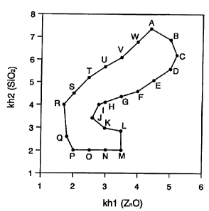
Figure 6 shows the numerical ranges of lrhl and kh2in which the electrome-
chanical coupling coe~cient I~falls in the range of 0.2 to 0.56% in Fig. 3,
the
propagation velocity v is 4,500 m/s or more in Fig. 4, and the frequency-
5 temperature property TCF falls in the range of -20 to +20 ppm/°C in
Fig. 5.
As is the case with Figs. 3 to 5, Fig. 6 shows a graph in a two-dimensional
orthogonal-coordinate system in which the axis of abscissa represents kh1 and
the axis of ordinate represents kb2. In Fig. 6, the numerical ranges of kh1
and
kh2 in which the electromechanical coupling coefficient I~falls in the range
of
10 0.2 to 0:56%, the propagation velocity v is 4,500 m/s or more, and the fre-
quency-temperature property TCFfalls in the range of -20 to +20 ppm/°C
are
given by a range produced by connecting points A, B, C, D, E, F, G, H, I, J,
I~ L,
M, N, O, P, Q, R, S, T, U, Y, W, and A in this order, the range of which
includes
the surrounding lengths of lines.
15 In the above description:
point A is given by the coordinates "kh1= 4.4 and kh2= 7.4";
point Bis given by the coordinates "khl = 5.0 and kh2= 6.9' ;
point Cis given by the coordinates "kh1= 5.2 and kh2= 6.2'
point Dis given by the coordinates "khl = 5.0 and kh2= 5.6';
point Eis given by the coordinates "kh1= 4.5 and kh2= 5.1' ;
point Fis given by the coordinates "kh1= 4.0 and kh2= 4.6' ;
point Gis given by the coordinates "khl = 3.5 and lrh2= 4.4";
point His given by the coordinates "khl = 3.0 and ~b2= 4.1";
CA 02374468 2001-11-27
16
point Iis given by the coordinates "khl = 2.8 and kh2= 4.0";
point Jis given by the coordinates "khl = 2.6 and kh2= 3.4";
point Kis given by the coordinates "kh1= 3.0 and kh2= 3.0' ;
point Lis given by the coordinates "kh1= 3.5 and Irh2= 2.9' ;
point Mis given by the coordinates "Irhl = 3.5 and kh2= 2.0' ;
point Nis given by the coordinates "khl = 3.0 and Irh2= 2.0' ;
point Ois given by the coordinates "kh1= 2.5 and kh2= 2.0' ;
point Pis given by the coordinates "kh1= 2.0 and kh2= 2.0' ;
point Qis given by the coordinates "kh1= 1.8 and kh2= 2.6";
point Ris given by the coordinates "khl = 1.7 and kh2= 4.0' ;
point Sis given by the coordinates "kh1= 2.0 and kh2= 4.5' ;
point Tis given by the coordinates "khl = 2.5 and kh2= 5.2";
point Uis given by the coordinates "Irh1= 3.0 and kh2= 5.T ;
point Vis given by the coordinates "kh1= 3.5 and kh2= 6.1"; and
point YYis given by the coordinates "khl = 4.0 and kh2= 6.8".
In other words, a SAW device having an electromechanical coupling coed-
dent, I~, of 0.2 to 0.56%, a propagation velocity, v, of 4,500 m/s or more,
and a
frequency-temperature property, TCF, of -20 to +20 ppm/°~C can be
obtained
when the SAW device is operated by using the fifth harmonic of the second mo-
de of the SAW and when the SAW device is constituted so that the numerical
ranges of kh1 and kh2can fall in a range produced by connecting points A, B,
C,
D, E, F, G,H,I,J,I~I~M,N, O, P, Q,IiyS, T, U, Y, W,andAasshowninFig.6
in this order, the range of which includes the surrounding lengths of lines.
CA 02374468 2001-11-27
17
When the SAW device is operated at a propagation velocity, v, of 4,500 to
6,500m/s, the digit electrodes of the IDTs can be formed with a width of 0.5
~c
m or more as can be derived from equation (1) above. This relatively wide
width
of the digit electrodes facilitates the production of the mTs, which then
facili-
tates mass production of the SAW device.
When the digit electrodes of the IDTs have a width of 0.5 ~ m or more and
the fifth harmonic of the second mode of the SAW has a center frequency of 5.0
to 11.3 GHz, more desirably 9.5 to 10.5 GHz, the above-described property
ranges of the electromechanical coupling coeff.cient .F~, the propagation
veloc-
ity v, and the frequency-temperature property TCFcan be obtained.
(Second Example)
The SAW device in this example was produced by procedures similar to those
in the First Example, with some conditions modified. It was intended that the
SAW device be operated at a center frequency of about 10 GHz.
In producing the SAW device, the thickness tz of the Zn0 layer was varied so
that the parameter khl could vary from 2.0 to 6.0, and the thicl~ess is of the
SiOalayer was varied so that the parameter kh2coul.d vary from 2.0 to 8Ø
As with the First Example, graphs showing the relationship of the electrome-
chanical coupling coe~cient I~, propagation velocity v, and frequency-
temperature property TCFto the thicknesses of the Zn0 and SiOa layers were
provided in a two-dimensional orthogonal-coordinate system. According to the-
se graphs, the numerical ranges of khl and kh2in which the electromechanical
coupling coe~cient I~falls in the range of 0.4 to 0.56%, the propagation veloc-
CA 02374468 2001-11-27
18
ity vis 4,500 m/s or more, and the frequency-temperature property TCFfalls in
the range of -20 to +20 ppm/°C are expressed in a graph plotted in a
two-
dimensional orthogonal-coordinate system as shown in Fig. 7.
In Fig. 7, the axis of abscissa represents khl and the axis of ordinate repre-
sents kh2. In Fig. 7, the numerical ranges of kh1 and kh2in which the electro-
mechanical coupling coe~cient XBfalls in the range of 0.4 to 0.56%, the propa-
gation velocity vis 4,500 mls or more, and the frequency-temperature property
TCFfalls in the range of -20 to +20 ppm/°C are given by a range
produced by
connecting points A, B, C, D, E, F, G, H, I, J, K, L, M, N, O, P, Q, B, S, T,
and A
in this order, the range of which includes the surrounding lengths of lines.
In the above description:
point A is given by the coordinates "khl = 4.4 and ~rh2= 6.9' ;
point Bis given by the.coordinates "kh1= 5.0 and kh2= 6.4' ;
point Cis given by the coordinates "Irh1= 5.2 and kh2= 6.2' ;
point Dis given by the coordinates "kh1= 5.0 and kb2= 5.6";
point Eis given by the coordinates "kh1= 4.6 and kh2= 5.2' ;
p oint Fis given by the coordinates "kh 1= 4.4 and kh2 = 5.0' ;
point G is given by the coordinates "kh 1= 4.0 and kb2 = 4.6' ;
point His given by the coordinates "Irhl = 3.5 and kh2= 4.4' ;
point Iis given by the coordinates "kh1= 3.0 and kh2= 4.1' ;
point Jis given by the coordinates "kh1= 2.8 and kh2= 4.0";
point Kis given by the coordinates "kh1= 2.6 and kh2= 3.4' ;
point Lis given by the coordinates "Irh1= 2.8 and kh2= 3.0";
CA 02374468 2001-11-27
19
point Mis given by the coordinates "khl = 3.2 and kh2= 2.4' ;
point Nis given by the coordinates "khl = 2.7 and kh2= 2.4' ;
point O is given by the coordinates "lrhl = 2.2 and kh2= 3.0' ;
point Pis given by the coordinates "kh1= 2.2 and Ich2= 3.5' ;
point Qis given by the coordinates "kh1= 2.5 and kh2= 4.7";
point Ris given by the coordinates "khl = 3.0 and kh2= 5.2";
point Sis given by the coordinates "kh1= 3.5 and kh2= 5.7"; and
p oint T is given by the coordinates "kh 1= 4.0 and kh2 = 6.3".
In other words, a SAW device having an electromechanical coupling coeffi-
dent, .I~, of 0.4 to 0.56%, a propagation velocity, v, of 4,500 m/s or more,
and a
frequency-temperature property, TCF, of -20 to +20 ppml°C can be
obtained
when the SAW device is constituted so that the numerical ranges of kh1 and
kh2can fall in a range produced by connecting points A, B, C, D, E, F, G, H,
I, J,
F~ L~ M, N, O, P, Q, R, S, T, and A as shown in Wig. 7 in this order, the
range of
which includes the surrounding lengths of lines.
When the SAW device is operated at a propagation velocity, v, of 4,500 to
6,500m/s, the digit electrodes of the mTs can be formed with a width of 0.5 ~c
m or more as can be derived from equation (1) above. This relatively wide
width
of the digit electrodes facilitates the production of the IDTs, which then
facili-
tates mass production of the SAW device.
When the digit electrodes of the mTs have a width of 0.5 ~u m or more and
the fifth harmonic of the second mode of the SAW has a center frequency of 5.0
to 11.3 GHz, more desirably 9.5 to 10.5 GHz, the above-described property
CA 02374468 2001-11-27
ranges of the electromechanical coupling coefficient ~; the propagation veloc-
ity v, and the frequency-temperature property TCFcan be obtained.
Industrial Applicability
As explained above, the present invention uses the fifth harmonic of the sec-
5 and mode of the SAW. This enables a SAW device to obtain an excellent propa-
gation property, electromechanical coupling coefficient, and frequency-
temperature property at the superhigh-frequency range. Moreover, the present
invention allows the use of wider digit electrodes in the IDTs, so that the
mass
production of the SAW device can be easily achieved.