Note: Descriptions are shown in the official language in which they were submitted.
CA 02374666 2001-11-21
WO 00/76911 PCT/US00/16382
IMPROVED METHODS OF FABRICATING
MICROELECTROMECHANICAL AND MICROFLUIDIC DEVICES
FIELD OF THE INVENTION
The invention relates to the field of design, development, and manufacturing
of
miniaturized chemical analysis devices and systems using
microelectromechanical
systems (MEMS) technology. In particular, the invention relates to
improvements in
process sequences for fabricating MEMS and microfluidic devices, including
electrospray
ionization, liquid chromatography, and integrated liquid
chromatography/electrospray
devices.
BACKGROUND OF THE INVENTION
Explosive growth in the demand for analysis of samples in combinatorial
chemistry, genomics, and proteomics is driving widespread efforts to increase
throughput,
increase accuracy, and to reduce volumes of reagents and samples required, as
well as
waste generated. Rapid developments in drug discovery and development are
creating
new demands on traditional analytical techniques. For example, combinatorial
chemistry
is often employed to discover new lead compounds, or to create variations of a
lead
compound. Combinatorial chemistry techniques can generate thousands or
millions of
compounds in combinatorial libraries within days or weeks. The generation of
enormous
amounts of genetic sequence data through new DNA sequencing methods in the
field of
genomics has allowed rapid identification of new targets for drug development
efforts.
There is therefore a critical need for rapid sequential analysis and
identification of
compounds that interact with a gene or gene product in order to identify
potential drug
candidates. Efficient proteomic screening methods are needed in order to
obtain the
pharmacokinetic profile of a drug early in the evaluation process, testing for
cytotoxicity,
specificity, and other pharmaceutical characteristics in high-throughput
assays instead of
in expensive animal testing and clinical trials. Testing such a large number
of compounds
for biological activity in a timely and efficient manner requires high-
throughput screening
methods that allow rapid evaluation of the characteristics of each candidate
compound.
Development of viable screening methods for these new targets will often
depend on the
availability of rapid separation and analysis techniques for analyzing the
results of assays.
CA 02374666 2001-11-21
WO 00/76911 PCT/US00/16382
2
Microchip-based separation devices have been developed for rapid analysis of
large numbers of samples. Compared to other conventional separation devices,
these
microchip-based separation devices have higher sample throughput, reduced
sample and
reagent consumption and reduced chemical waste. Liquid flow rate for microchip-
based
separation devices range from approximately 1-300 nanoliters (nL) per minute
for most
applications.
Examples of microchip-based separation devices include those for capillary
electrophoresis (CE), capillary electrochromatography (CEC) and high-
performance liquid
chromatography (HPLC). See Harnson et al., Science 1993, 261, 895-897;
Jacobsen et
al., Anal. Chem. 1994, 66, 1114-1118; and Jacobsen et al., Anal. Chem. 1994,
66, 2369-
2373. Such separation devices are capable of fast analyses and provide
improved
precision and reliability compared to other conventional analytical
instruments.
He et al., Anal. Chem. 1998, 70, 3790-3797 describes the fabrication of
chromatography columns on quartz wafers and reports an evaluation of column
efficiency
in the capillary electrochromatography (CEC) mode. The fabrication sequence
described
relies partly on standard, parallel microfabrication operations to create
multiple separation
channels and structures therein on which stationary phase materials may be
coated.
However, methods described for enclosing the separation channels as well as
for providing
fluidic access to and egress from the channels are decidedly non-standard and
unsuitable
for integration in a conventional, high-productivity microfabrication
sequence.
Liquid chromatography (LC) is a well-established analytical method for
separating
components of a fluid for subsequent analysis and/or identification.
Traditionally, liquid
chromatography utilizes a separation column, such as a cylindrical tube,
filled with tightly
packed beads, gel or other appropriate particulate material to provide a large
surface area.
The large surface area facilitates fluid interactions with the particulate
material, resulting
in separation of components of the fluid as it passes through the separation
column, or
channel. The separated components may be analyzed spectroscopically or may be
passed
from the liquid chromatography column into other types of analytical
instruments for
analysis.
CA 02374666 2001-11-21
WO 00/76911 PCT/US00/16382
3
The separated product of such separation devices may be introduced as a liquid
sample to a device that is used to produce electrospray ionization. The
electrospray device
may be interfaced to an atmospheric pressure ionization mass spectrometer (API-
MS) for
analysis of the electrosprayed fluid.
A schematic of an electrospray system 10 is shown in FIG. 1. An electrospray
is
produced when a sufficient electrical potential difference VsP,.ay is applied
between a
conductive or partly conductive fluid exiting a capillary orifice and an
electrode so as to
generate a concentration of electric field lines emanating from the tip or end
of a capillary
2 of an electrospray device. When a positive voltage Vsp,.ay is applied to the
tip of the
capillary relative to an extracting electrode 4, such as one provided at the
ion-sampling
orifice to the mass spectrometer, the electric field causes positively-charged
ions in the
fluid to migrate to the surface of the fluid at the tip of the capillary 2.
When a negative
voltage VsPray is applied to the tip of the capillary relative to the
extracting electrode 4,
such as one provided at the ion-sampling orifice to the mass spectrometer, the
electric field
causes negatively-charged ions in the fluid to migrate to the surface of the
fluid at the tip
of the capillary 2.
When the repulsion force of the solvated ions exceeds the surface tension of
the
fluid sample being electrosprayed, a volume of the fluid sample is pulled into
the shape of
a cone, known as a Taylor cone 6, which extends from the tip of the capillary
2. Small
charged droplets 8 are formed from the tip of the Taylor cone 6, which are
drawn toward
the extracting electrode 4. This phenomenon has been described, for example,
by Dole et
al., J. Chem. Phys. 1968, 49, 2240 and Yamashita and Fenn, J. Phys. Chem.
1984, 88,
4451. The potential voltage required to initiate an electrospray is dependent
on the surface
tension of the solution as described by, for example, Smith, IEEE Trans. Ind.
Appl. 1986,
IA-22, 527-535. Typically, the electric field is on the order of approximately
106 V/m.
The physical size of the capillary determines the density of electric field
lines necessary to
induce electrospray.
The process of electrospray ionization at flow rates on the order of
nanoliters per
minute has been referred to as "nanoelectrospray." Electrospray into the ion-
sampling
orifice of an API mass spectrometer produces a quantitative response from the
mass
CA 02374666 2001-11-21
WO 00/76911 PCT/US00/16382
4
spectrometer detector due to the analyte molecules present in the liquid
flowing from the
capillary. It is desirable to provide an electrospray ionization device for
integration
upstream with microchip-based separation devices and for integration
downstream with
API-MS instruments.
The development of miniaturized devices for chemical analysis - and, further,
for
synthesis and fluid manipulation - is motivated by the prospects of improved
efficiency,
reduced cost, and enhanced accuracy. Efficient, reliable manufacturing
processes are a
critical requirement for the cost-effective, high-volume production of devices
that are
targeted at high-volume, high-throughput test markets.
Attempts have been made to fabricate an electrospray device that produces
nanoelectrospray. For example, Wilm and Mann, Anal. Chem. 1996, 68, 1-8
describes
the process of electrospray from fused silica capillaries drawn to an inner
diameter of
2-4 ~m at flow rates of 20 nL/min. Specifically, a nanoelectrospray at 20
nL/min was
achieved from a 2 ~,m inner diameter and 5 pm outer diameter pulled fused-
silica capillary
with 600-700 V at a distance of 1-2 mm from the ion-sampling orifice of an API
mass
spectrometer.
Ramsey et al., Anal. Chem. 1997, 69, 1174-1178 describes nanoelectrospray at
90 nL/min from the edge of a planar glass microchip with a closed separation
channel
10 pm deep, 60 ~tm wide and 33 mm in length using electroosmotic flow. A
voltage of
4.8 kV was applied to the fluid exiting the closed separation channel on the
edge of the
microchip to initiate electrospraying, with the edge of the chip at a distance
of 3-5 mm
from the ion-sampling orifice of an API mass spectrometer. Approximately 12 nL
of the
sample fluid collected at the edge of the chip before a Taylor cone formed and
initiated a
stable nanoelectrospray from the edge of the microchip. However, collection of
approximately 12 nL of the sample fluid results in re-mixing of the fluid,
thereby undoing
the separation done in the separation channel. Re-mixing at the edge of the
microchip
causes band broadening, fundamentally limiting its applicability for
nanoelectrospray-
mass spectrometry for analyte detection. Thus, electrospraying from the edge
of this
microchip device after capillary electrophoresis or capillary
electrochromatography
separation is rendered impractical. Furthermore, because this device provides
a flat
CA 02374666 2001-11-21
WO 00/76911 PCT/US00/16382
surface, and thus a relatively small amount of physical asperity for the
formation of the
electrospray, the device requires an impracticably high voltage to initiate
electrospray, due
to poor field line concentration.
Xue et al., Anal. Chem. 1997, 69, 42630 describes a stable nanoelectrospray
5 from the edge of a planar glass microchip with a closed channel 25 ~m deep,
60 pm wide
and 35-50 mm in length. A potential of 4.2 kV was applied to the fluid exiting
the closed
separation channel on the edge of the microchip to initiate electrospraying,
with the edge
of the chip at a distance of 3-8 mm from the ion-sampling orifice of an API
mass
spectrometer. A syringe pump was utilized to deliver the sample fluid to the
glass
electrospray microchip at a flow rate between 100-200 nLJmin. The edge of the
glass
microchip was treated with a hydrophobic coating to alleviate some of the
difficulties
associated with electrospraying from a flat surface and to thereby improve the
stability of
the nanoelectrospray. Electrospraying in this manner from a flat surface,
however, again
results in poor field line concentration and yields an inefficient
electrospray.
In all of the devices described above, edge-spraying from a chip is a poorly
controlled process due to the inability to rigorously and repeatably determine
the physical
form of the chip's edge. In another embodiment of edge-spraying, ejection
nozzles, such
as small segments of drawn capillaries, are separately and individually
attached to the
chip's edge. This process imposes space constraints in chip design and is
inherently cost-
inefficient and unreliable, making it unsuitable for manufacturing.
Desai et al., 1997 International Conference on Solid-State Sensors and
Actuators,
Chicago, June 16-19, 1997, 927-930 describes a mufti-step process to generate
a nozzle
on the edge of a silicon microchip 1-3 ~m in diameter or width and 40 ~m in
length. A
voltage of 4 kV was applied to the entire microchip at a distance of 0.25-0.4
mm from the
ion-sampling orifice of an API mass spectrometer. This nanoelectrospray nozzle
reduces
the dead volume of the sample fluid. However, the extension of the nozzle from
the edge
of the microchip makes the nozzle susceptible to accidental breakage. Because
a
relatively high spray voltage was utilized and the nozzle was positioned in
very close
proximity to the mass spectrometer sampling orifice, a poor field line
concentration and a
low efficient electrospray were achieved.
CA 02374666 2001-11-21
WO 00/76911 PCT/US00/16382
6
Wang et al., 1999 IEEE International Conference on Micro Electro Mechanical
Systems, Orlando, January 17-21, 1999, 523-528 describes a polymer-based
electrospray
structure designed to spray from the edge of the chip, essentially replacing
the
mechanically fragile silicon nitride nozzle of Desai et al. with a polymeric
nozzle. While
the polymer substitution provides a significant improvement in mechanical
reliability,
additional non-standard processing materials and operations are required,
making the
fabrication of the structures incompatible with standard high-volume
manufacturing
facilities. Further, the presence of the polymeric material seriously limits
the nature of
subsequent processing operations and precludes high-temperature processing
altogether.
Concerns regarding sample contamination by monomeric residues in the polymer
remain
unresolved.
Thus, it is also desirable to provide an electrospray ionization device with
controllable spraying and a method for producing such a device that is easily
reproducible
and manufacturable in high volumes.
U. S. Pat. Appl. Ser. No. 09/156,037 (Moon et al.) describes electrospray
ionization (ESI), liquid chromatography (LC), and integrated LC/ESI devices
and systems
and fabrication sequences to make them in silicon by reactive-ion etching.
That
application discloses methods of designing and fabricating those devices and
similar ones
in a manner that is consistent with well-established, cost-efficient, high-
volume
manufacturing operations. However, there are several aspects of the
fabrication sequences
and designs that potentially limit manufacturing yield. First, separation
posts formed for
purposes of liquid chromatography are subject to damaging mechanical stresses
due to
coating of additional films, wet immersions, and abrasion and clamping in the
course of
processing operations after formation of the separation posts. Second, etch
lag in
electrospray nozzle channels makes it difficult to complete the channel while
controlling
the height of the nozzle. Third, the formation of electrical contacts to the
substrate in the
presence of significant topographical steps of more than 1-2 pm is problematic
due to an
inability to uniformly and continuously coat photoresist for purposes of
lithographic
patterning and subsequent etching. Thus, improved processing operations and
sequences
are desired in order to ensure the high-yield manufacturability of such
devices and
CA 02374666 2001-11-21
WO 00/76911 PCT/US00/16382
7
systems. Further, such processing improvements that can be widely applied to a
variety of
MEMS and microfluidic devices and systems are highly desired.
SUMMARY OF THE INVENTION
The aspects of the present invention described herein have been shown to
significantly improve prior approaches to fabricating MEMS and microfluidic
devices.
They have been successfully used to overcome the specific yield-limiting
problems
discussed hereinabove. They may be used individually or severally to greatly
improve the
component of manufacturing yield attributed to wafer-level processing for many
microfabricated devices. In particular, some or all of them may be used to
improve the
yield of electrospray ionization (ESI), liquid chromatography (LC), and
integrated
LC/ESI devices.
The present invention provides three sequences of process steps that may be
individually or severally integrated with other standard silicon processing
operations to
fabricate MEMS and microfluidic devices and systems with enhanced
manufacturability.
Each of the three aspects of the present invention provides relief to design
and process
integration constraints and overcomes limitations deriving from interacting
process
operations. In general, these constraints and limitations are surmounted by
rendering the
device or system insensitive to problematic operations and/or by decoupling
design and
process interactions. Each of the aspects is independent from the others. Any
two or all of
the aspects may be used in concert to relieve a multiplicity of constraints.
The yield-
enhancing effects of the several aspects are found to have a cumulative,
positive impact on
manufacturing yield.
The three fundamental aspects of this invention are referred to herein as
latent
masking, simultaneous multi-level etching (SMILE), and delayed LOCOS. Each of
these
three fundamental aspects generally comprises a sequence of silicon processing
steps that
may be incorporated in a complete sequence for the fabrication of MEMS and
microfluidic
devices and systems. Three additional aspects of the present invention are
derived aspects
that incorporate one or more of the three fundamental aspects in integrated
processes to
fabricate specific MEMS or microfluidic devices or systems. Each of the
derived aspects
CA 02374666 2001-11-21
WO 00/76911 PCT/US00/16382
of the present invention provides a novel fabrication process that
significantly improves
fabrication reliability and manufacturing yield.
The first fundamental aspect of the present invention, designated herein as
latent
masking, provides a means by which a mask may be created at one stage of the
overall
process but then held abeyant pending its ultimate use to mask an etch of an
underlying
film or substrate after a sequence of intervening process steps. During the
intervening
steps, the mask remains latent and unperturbed, neither affecting the
operations conducted
nor being affected by them. The latent mask is preferably formed in a film of
silicon
oxide or, alternatively, is formed in a material such as a polyimide. The
salient
characteristic of the masking material is its resistance to wet and/or dry
processing steps
after its formation and prior to its ultimate use.
In the preferred embodiment, a silicon oxide film is patterned to create the
latent
mask by a sequence of standard lithographic processing steps, including
coating, exposure,
and development of a photoresist film, followed by a reactive-ion etch of the
underlying
oxide film, thereby transferring the photoresist pattern to the oxide layer.
In an alternative
embodiment, a more durable masking material such as polyimide may be coated
and
patterned lithographically, then cured at elevated temperature.
Once the latent mask has been created, a sequence of processing operations may
be
performed before using the mask. After those intervening process steps, the
mask is used
to protect certain areas of an underlying film or substrate during the etching
of that
film/substrate, thereby transferring the mask pattern into the underlying
film/substrate.
Preferably, the latent mask is composed of silicon oxide and is used to mask
the etch of an
underlying silicon substrate by reactive-ion etching. In alternative
embodiments of the
invention, the etching may be done using wet chemical etching techniques
and/or the
underlying film/substrate may be a material other than silicon, the principal
requirement
being the compatibility of the etch mask material with the chosen method of
etching.
One advantage of latent masking as described herein is that the latent mask
does
not interfere with subsequent lithographic patterning steps. A second
advantage is that the
low-profile latent mask is not susceptible to damage from abrasion stresses.
Yet another,
and decisive, advantage of latent masking is that the use of the mask may be
placed at a
CA 02374666 2001-11-21
WO 00/76911 PCT/US00/16382
9
late enough stage in the overall process to ensure that the resulting fragile
structures are
not subjected to damaging stresses by subsequent operations.
The second fundamental aspect of the present invention, designated herein as
simultaneous multi-level etching (SMILE), provides a means of etching two
different
patterns into, preferably, a silicon substrate such that the final etched
depths of the two
patterns may be independently controlled. The essence of this aspect is that
the etching of
one pattern may be advanced relative to a second pattern by beginning to etch
the former
first pattern without simultaneously etching the second pattern. After an
initial etch of the
first pattern alone, both patterns are etched simultaneously.
Lithographic patterning creates a first pattern in a photoresist mask. The
first
pattern is transferred to an underlying silicon oxide layer by reactive-ion
etching or wet
etching, after which the photoresist mask is removed. A second lithographic
patterning
step is then done to create a second photoresist mask that comprises both the
first and
second patterns. After the patterning of the second photoresist mask, an
opening exists in
the photoresist mask and silicon oxide film corresponding to the first
pattern, whereas the
second pattern in the photoresist mask is open only to the underlying silicon
oxide layer.
A silicon etch is done by reactive-ion etching in the openings to the silicon
substrate
corresponding to the first pattern, thereby providing the desired advanced
etch for the first
pattern. Next, an oxide etch is done to open the second pattern through the
silicon oxide to
the silicon substrate. Finally, a second silicon etch is done, proceeding
simultaneously in
both the first and second patterns, after which any remaining photoresist mask
may be
removed.
This aspect of the present invention may be used to compensate for etch-rate
lag
and to thereby attain equal etch depths in all features. Alternatively, two
patterns may be
etched to two different depths. Further, the manufacturing yield of a second
pattern may
be significantly improved compared to standard sequential lithographic
patterning and
etch sequences. The limited topography created by the first patterning
sequence does not
adversely affect the deposition of a second photoresist film. An additional
advantage over
standard sequential lithographic patterning and etch sequences is a savings of
up to half
CA 02374666 2001-11-21
WO 00/76911 PCT/US00/16382
the total sequential etching time as a result of the two patterns being
partially etched
simultaneously.
SMILE may be used to compensate for etch rate lag, a phenomenon observed in
reactive-ion etching in which the etch rate in a small opening is retarded
relative to that in
a larger opening. By appropriately advancing the etching of a small first
pattern, for
example, the subsequent simultaneous etch of the first pattern and a larger
second pattern
may be used to attain an equal final depth in both patterns. Alternatively, an
etch of a first
pattern may be advanced relative to a second pattern of equivalent geometry to
result in a
deeper final depth for the first pattern.
10 The third fundamental aspect of the present invention, designated herein as
delayed
LOCOS, generally comprises a sequence of processing steps to provide
electrical access to
an otherwise isolated substrate. This aspect of the invention may be used,
preferably, to
create contact holes through a silicon oxide insulating layer to an underlying
silicon
substrate. The essence of this aspect of the invention is that patterns that
will ultimately
correspond to the required contact holes to the substrate are created at an
early stage in an
overall fabrication sequence. Rather than completing the opening of the
contact holes and
forming the contacts immediately after patterning, the contact pattern remains
abeyant
while other standard silicon processing operations are executed. At a later
stage in the
process, the latent contact pattern is used to create the desired contact
holes.
This aspect of the present invention is a modification to and improvement upon
a
standard silicon processing sequence known as LOCaI Oxidation of Silicon, or
LOCOS.
A relatively thin oxide film is grown, followed by the deposition of a thicker
silicon
nitride film. Standard lithographic procedures and reactive-ion etching are
used to pattern
the silicon nitride film. The pattern is such that nitride remains where
contact holes are
ultimately to be formed. The nitride pattern thus formed remains in place
during
subsequent processing.
When a stage is reached in the overall process - generally, after all high
temperature (>400°C) processing has been completed - where electrical
contacts to the
silicon substrate must be formed, the silicon nitride and the underlying thin
oxide layer are
CA 02374666 2001-11-21
WO 00/76911 PCTNS00/16382
11
removed to expose the silicon substrate. Metal, preferably aluminum, is then
deposited
and may be patterned by standard lithographic and etching techniques.
This aspect of the present invention has the advantage that the nitride
patterning is
done at an early stage in the process when there is little or no surface
topography to
interfere with the uniform and continuous coating of photoresist for
lithographic
patterning. This is favored over the standard alternative approach in which
contact hole
patterning is done immediately prior to metallization, generally in the
presence of
significant and limiting surface topography.
A fourth aspect of the present invention provides an improved process for
fabricating an integrated liquid chromatography/electrospray ionization
(LC/ESI) device.
All three of the fundamental aspects of this invention are incorporated in the
fabrication
sequence to significantly improve fabrication reliability and manufacturing
yield. In the
preferred embodiment, the integrated process produces an LC/ESI device
generally
comprising a silicon substrate defining an introduction orifice and a nozzle
on an ejection
surface such that electrospray generated by the ESI component is generally
approximately
perpendicular to the ejection surface; a fluid reservoir and a separation
channel on a
separation surface; at least one controlling electrode electrically contacting
the substrate
through the oxide layer on the ejection surface; and a second substrate
attached to the
separation surface of the first substrate so as to enclose the fluid reservoir
and separation
channel. The second substrate may also define an electrode or electrodes with
which to
control fluid motion in the LC/ESI device. The LC/ESI device is integrated
such that the
exit of the separation channel forms a homogeneous interface with the entrance
to the
nozzle. All surfaces of the device preferably have a layer of silicon oxide to
electrically
isolate the liquid sample from the substrate and to provide for
biocompatibility.
A fifth aspect of the present invention provides an improved process for
fabricating
an electrospray ionization (ESI) device. Two of the fundamental aspects of the
present
invention, simultaneous mufti-level etching and delayed LOCOS, are
incorporated in the
fabrication sequence to significantly improve fabrication reliability and
manufacturing
yield. In the preferred embodiment, the integrated process produces an ESI
device
generally comprising a silicon substrate defining a nozzle and surrounding
recessed region
CA 02374666 2001-11-21
WO 00/76911 PCT/US00/16382
12
on an ejection surface, an entrance orifice on the opposite surface (the
injection surface),
and a nozzle channel extending between the entrance orifice and nozzle such
that the
electrospray generated by the electrospray device is directed generally
perpendicularly to
the ejection surface. All surfaces of the ESI device preferably have a layer
of silicon oxide
to electrically isolate the liquid sample from the substrate and to provide
for
biocompatibility.
A sixth aspect of the present invention provides an improved process for
fabricating a liquid chromatography (LC) device. Two of the fundamental
aspects of the
present invention - latent masking and delayed LOCOS - are incorporated in the
fabrication sequence to significantly improve fabrication reliability and
manufacturing
yield. In the preferred embodiment, the integrated process produces an LC
device
generally comprising a silicon substrate defining an introduction channel
between an
entrance orifice and a reservoir, a separation channel between the reservoir
and a
separation channel terminus, and an exit channel between the separation
channel terminus
and an exit orifice; the LC device further comprising a second substrate
attached to the
separation surface of the first substrate so as to enclose the reservoir and
separation
channel. All surfaces of the LC device preferably have a layer of silicon
oxide to
electrically isolate the liquid sample from the substrate and to provide for
biocompatibility.
BRIEF DESCRIPTION OF THE DRAWINGS
Fig. 1 shows a schematic of an electrospray system;
Fig. 2A shows a schematic cross-sectional view of the application of stress to
a
silicon structure;
Fig. 2B shows a schematic cross-sectional view of the damage to a silicon
structure
resulting from application of stress;
Fig. 3A shows a cross-sectional view of the latent masking process sequence;
Fig. 3B shows a plan view of the latent masking process sequence;
CA 02374666 2001-11-21
WO 00/76911 PCT/US00/16382
13
Fig. 3C shows a cross-sectional view of the latent masking process sequence;
Fig. 3D shows a cross-sectional view of the latent masking process sequence;
Fig. 4A shows a cross-sectional view of an alternative embodiment of the
latent
masking aspect of the present invention;
Fig. 4B shows a cross-sectional view of an alternative embodiment of the
latent
masking aspect of the present invention;
Fig. 5A shows a conventional process sequence for fabricating separation
posts;
Fig. 5B shows a latent masking block process sequence for fabricating
separation
posts;
Fig. 6A shows a scanning electron micrograph of separation posts fabricated
using
conventional processes;
Fig. 6B shows a scanning electron micrograph of separation posts fabricated
using
latent masking processes;
Fig. 7A shows a plan view of the simultaneous multi-level etching (SMILE)
processsequence;
Fig. 7B a cross-sectional view of the simultaneous multi-level etching (SMILE)
processsequence;
Fig. 7C shows a plan view of the simultaneous mufti-level etching (SMILE)
processsequence;
Fig. 7D shows a cross-sectional view of the simultaneous mufti-level etching
(SMILE) process sequence;
Fig. 8 shows a cross-sectional view of the simultaneous mufti-level etching
(SMILE) process sequence;
Fig. 9 shows a cross-sectional view of the simultaneous mufti-level etching
(SMILE) process sequence;
CA 02374666 2001-11-21
WO 00/76911 PCT/US00/16382
14
Fig. 10 shows a cross-sectional view of the simultaneous multi-level etching
(SMILE) process sequence;
Fig. 11A shows a cross-sectional view of one of three alternative outcomes
from
the SMILE process;
Fig. 11B shows a cross-sectional view of one of three alternative outcomes
from
the SMILE process;
Fig. 11C shows a cross-sectional view of one of three alternative outcomes
from
the SMILE process;
Fig. 12A shows a plan view of a nozzle structure;
Fig. 12B shows a cross-sectional view of a nozzle structure;
Fig. 13A shows a cross-sectional view of an etched nozzle structure without
compensation for etch lag;
Fig. 13B shows a cross-sectional view of an etched nozzle structure with
compensation for etch lag;
Fig. 14 shows a scanning electron micrograph of a nozzle structure fabricated
using the SMILE process;
Fig. 15 shows a cross-sectional view of a nozzle and through-substrate channel
fabricated using the SMILE process to overcome certain limitations on design
geometries;
Fig. 16A shows a plan view of an alternative embodiment of the SMILE process
sequence to independently control etch depths of three patterns;
Fig. 16B shows a cross-sectional view of an alternative embodiment of the
SMILE
process sequence to independently control etch depths of three patterns;
Fig. 16C shows a plan view of an alternative embodiment of the SMILE process
sequence to independently control etch depths of three patterns;
CA 02374666 2001-11-21
WO 00/76911 PCT/US00/16382
Fig. 16D shows a cross-sectional view of an alternative embodiment of the
SMILE
process sequence to independently control etch depths of three patterns;
Fig. 16E shows a cross-sectional view of an alternative embodiment of the
SMILE
process sequence to independently control etch depths of three patterns;
5 Fig. 16F shows a cross-sectional view of an alternative embodiment of the
SMILE
process sequence to independently control etch depths of three patterns;
Fig. 16G shows a cross-sectional view of an alternative embodiment of the
SMILE
process sequence to independently control etch depths of three patterns;
Fig. 16H shows a plan view of an alternative embodiment of the SMILE process
10 sequence to independently control etch depths of three patterns;
Fig. 16I shows a cross-sectional view of an alternative embodiment of the
SMILE
process sequence to independently control etch depths of three patterns;
Fig. 17 shows the delayed LOCOS block process sequence;
Fig. 18 shows a cross-sectional view of the initial steps of the delayed LOCOS
15 process;
Fig. 19 shows a cross-sectional view of the initial steps of the delayed LOCOS
process;
Fig. 20 shows a cross-sectional view of the initial steps of the delayed LOCOS
process;
Fig. 21 shows data relating to the oxidation of silicon nitride;
Fig. 22A shows a cross-sectional view of an alternative method for silicon
nitride
removal to open contact holes;
Fig. 22B shows a cross-sectional view of an alternative method for silicon
nitride
removal to open contact holes;
CA 02374666 2001-11-21
WO 00/76911 PCT/US00/16382
16
Fig. 22C shows a cross-sectional view of an alternative method for silicon
nitride
removal to open contact holes;
Fig. 23 shows a cross-sectional view of the bird's beak region at the edge of
a
contact hole;
Fig. 24 shows a block process sequence for fabricating an integrated LC/ESI
device;
Fig. 25A shows a plan view of a completed LC/ESI device;
Fig. 25B shows a cross-sectional view of a completed LC/ESI device;
Fig. 25C shows a cross-sectional view of a completed LC/ESI device;
Fig. 26A shows a plan view of the initial process steps relating to the
delayed
LOCOS aspect of the invention, as part of a fabrication sequence for an
integrated LC/ESI
device;
Fig. 26B shows a cross-sectional view of the initial process steps relating to
the
delayed LOCOS aspect of the invention, as part of a fabrication sequence for
an integrated
LC/ESI device;
Fig. 26C shows a cross-sectional view of the initial process steps relating to
the
delayed LOCOS aspect of the invention, as part of a fabrication sequence for
an integrated
LC/ESI device;
Fig. 27A shows a plan view of the initial process steps relating to the
delayed
LOCOS aspect of the invention, as part of a fabrication sequence for an
integrated LC/ESI
device;
Fig. 27B shows a cross-sectional view of the initial process steps relating to
the
delayed LOCOS aspect of the invention, as part of a fabrication sequence for
an integrated
LC/BSI device;
Fig. 28 shows a cross-sectional view of further process steps in the
fabrication of
an integrated LC/ESI device;
CA 02374666 2001-11-21
WO 00/76911 PCT/US00/16382
17
Fig. 29 shows a cross-sectional view of further process steps in the
fabrication of
an integrated LC/ESI device;
Fig. 30A shows a plan view of further process steps in the fabrication of an
integrated LC/ESI device;
Fig. 30B shows a cross-sectional view of further process steps in the
fabrication of
an,integrated LC/BSI device;
Fig. 31 shows a cross-sectional view of process steps relating to the
definition of
an oxide mask for latent masking in the fabrication of an integrated LC/ESI
device;
Fig. 32A shows a plan view of process steps relating to the definition of an
oxide
mask for latent masking in the fabrication of an integrated LC/ESI device;
Fig. 32B shows a cross-sectional view of process steps relating to the
definition of
an oxide mask for latent masking in the fabrication of an integrated LC/ESI
device;
Fig. 33 shows a cross-sectional view of process steps relating to the
formation of
fluid reservoirs and through-wafer channels in the fabrication of an
integrated LC/ESI
device;
Fig. 34A shows a plan view of process steps relating to the formation of fluid
reservoirs and through-wafer channels in the fabrication of an integrated
LC/ESI device;
Fig. 34B shows a cross-sectional view of process steps relating to the
formation of
fluid reservoirs and through-wafer channels in the fabrication of an
integrated LC/ESI
device;
Fig. 35 shows a cross-sectional view of process steps relating to the
formation of
fluid reservoirs and through-wafer channels in the fabrication of an
integrated LC/ESI
device;
Fig. 36 shows a cross-sectional view of process steps relating to nozzle and
through-substrate channel formation using the SMILE aspect of the invention,
as part of a
continuing fabrication sequence for an integrated LC/ESI device;
CA 02374666 2001-11-21
WO 00/76911 PCT/US00/16382
18
Fig. 37A shows a plan view of process steps relating to nozzle and through-
substrate channel formation using the SMILE aspect of the invention, as part
of a
continuing fabrication sequence for an integrated LC/ESI device;
Fig. 37B shows a cross-sectional view of process steps relating to nozzle and
through-substrate channel formation using the SMILE aspect of the invention,
as part of a
continuing fabrication sequence for an integrated LC/ESI device;
Fig. 38 shows a cross-sectional view of process steps relating to nozzle and
through-substrate channel formation using the SMILE aspect of the invention,
as part of a
continuing fabrication sequence for an integrated LC/ESI device;
Fig. 39A shows a plan view of process steps relating to nozzle and through-
substrate channel formation using the SMILE aspect of the invention, as part
of a
continuing fabrication sequence for an integrated LC/ESI device;
Fig. 39B shows a cross-sectional view of process steps relating to nozzle and
through-substrate channel formation using the SMILE aspect of the invention,
as part of a
continuing fabrication sequence for an integrated LC/ESI device;
Fig. 40 shows a cross-sectional view of process steps relating to nozzle and
through-substrate channel formation using the SMILE aspect of the invention,
as part of a
continuing fabrication sequence for an integrated LC/ESI device;
Fig. 41 shows a cross-sectional view of process steps relating to nozzle and
through-substrate channel formation using the SMILE aspect of the invention,
as part of a
continuing fabrication sequence for an integrated LC/ESI device;
Fig. 42A shows a plan view of process steps relating to completion of the
latent
masking aspect of the invention in the fabrication of an integrated LC/ESI
device;
Fig. 42B shows a cross-sectional view of process steps relating to completion
of
the latent masking aspect of the invention in the fabrication of an integrated
LC/ESI
device;
CA 02374666 2001-11-21
WO 00/76911 PCT/US00/16382
19
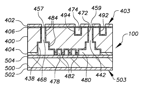
Fig. 43 shows a cross-sectional view of an integrated LC/ESI device after
passivation oxidation;
Fig. 44A shows an exploded perspective view of the first silicon substrate and
a
cover substrate in the fabrication of an integrated LC/ESI device;
Fig. 44B shows an exploded cross-sectional view of the first silicon substrate
and a
cover substrate in the fabrication of an integrated LC/ESI device;
Fig. 45 shows a cross-sectional view of the formation of electrical contact to
the
substrate in the fabrication of an integrated LC/ESI device;
Fig. 46 shows a cross-sectional view of the formation of electrical contact to
the
substrate in the fabrication of an integrated LC/ESI device;
Fig. 47A shows a plan view of the formation of electrical contact to the
substrate in
the fabrication of an integrated LC/BSI device;
Fig. 47B shows a cross-sectional view of the formation of electrical contact
to the
substrate in the fabrication of an integrated LC/ESI device;
Fig. 47C shows a cross-sectional view of the formation of electrical contact
to the
substrate in the fabrication of an integrated LC/ESI device;
Fig. 48A shows an exploded perspective view of an alternative method of
metallization involving the use of a shadow mask in the fabrication of an
integrated
LC/ESI device;
Figs. 48B shows an exploded cross-sectional view of an alternative method of
metallization involving the use of a shadow mask in the fabrication of an
integrated
LC/ESI device;
Fig. 49 shows a block process sequence for fabricating an ESI device;
Fig. 50A shows a plan view of a completed ESI device;
Figs. 50B shows a cross-sectional view of a completed ESI device;
CA 02374666 2001-11-21
WO 00/76911 PCT/US00/16382
Fig. 51A shows a plan view of the initial process steps relating to the
delayed
LOCOS aspect of the invention, as part of a fabrication sequence for an ESI
device;
Fig. 51B shows a cross-sectional view of the initial process steps relating to
the
delayed LOCOS aspect of the invention, as part of a fabrication sequence for
an ESI
5 device;
Fig. 51C shows a cross-sectional view of the initial process steps relating to
the
delayed LOCOS aspect of the invention, as part of a fabrication sequence for
an ESI
device;
Fig. 52A shows a plan view of the initial process steps relating to the
delayed
10 LOCOS aspect of the invention, as part of a fabrication sequence for an ESI
device;
Fig. 52B shows a cross-sectional view of the initial process steps relating to
the
delayed LOCOS aspect of the invention, as part of a fabrication sequence for
an ESI
device;
Fig. 53 shows a cross-sectional view of further process steps in the
fabrication of
15 an ESI device;
Fig. 54 shows a cross-sectional view of further process steps in the
fabrication of
an ESI device;
Fig. SSA shows a plan view of further process steps in the fabrication of an
ESI
device;
20 Fig. SSB shows a cross-sectional view of further process steps in the
fabrication of
an ESI device;
Fig. 56 shows a cross-sectional view of process steps relating to nozzle and
through-substrate channel formation using the SMILE aspect of the invention,
as part of a
continuing fabrication sequence for an ESI device;
CA 02374666 2001-11-21
WO 00/76911 PCT/US00/16382
21
Fig. 57A shows a plan view of process steps relating to nozzle and through-
substrate channel formation using the SMILE aspect of the invention, as part
of a
continuing fabrication sequence for an ESI device;
Fig. 57B shows a cross-sectional view of process steps relating to nozzle and
through-substrate channel formation using the SMILE aspect of the invention,
as part of a
continuing fabrication sequence for an ESI device;
Fig. 58 shows a cross-sectional view of process steps relating to nozzle and
through-substrate channel formation using the SMILE aspect of the invention,
as part of a
continuing fabrication sequence for an ESI device;
Fig. 59A shows a plan view of process steps relating to nozzle and through-
substrate channel formation using the SMILE aspect of the invention, as part
of a
continuing fabrication sequence for an ESI device;
Fig. 59B shows a cross-sectional view of process steps relating to nozzle and
through-substrate channel formation using the SMILE aspect of the invention,
as part of a
continuing fabrication sequence for an ESI device;
Fig. 60 shows a cross-sectional view of process steps relating to nozzle and
through-substrate channel formation using the SMILE aspect of the invention,
as part of a
continuing fabrication sequence for an ESI device;
Fig. 61 shows a cross-sectional view of process steps relating to nozzle and
through-substrate channel formation using the SMILE aspect of the invention,
as part of a
continuing fabrication sequence for an ESI device;
Fig. 62 shows a cross-sectional view of an ESI device after passivation
oxidation;
Fig. 63 shows a cross-sectional view of the formation of electrical contact to
the
substrate in the fabrication of an ESI device;
Fig. 64 shows a cross-sectional view of the formation of electrical contact to
the
substrate in the fabrication of an ESI device;
CA 02374666 2001-11-21
WO 00/76911 PCT/US00/16382
22
Fig. 65A shows a plan view of the formation of electrical contact to the
substrate in
the fabrication of an ESI device;
Fig. 65B shows a cross-sectional view of the formation of electrical contact
to the
substrate in the fabrication of an ESI device;
Fig. 66 shows a cross-sectional view of the formation of electrical contact to
the
substrate in the fabrication of an ESI device;
Fig. 67A shows a plan view of the formation of electrical contact to the
substrate in
the fabrication of an ESI device;
Fig. 67B shows a cross-sectional view of the formation of electrical contact
to the
substrate in the fabrication of an ESI device;
Fig. 68 shows a perspective view of a fluid delivery system and an ESI device;
Fig. 69A shows an exploded perspective of an alternative method of
metallization
involving the use of a shadow mask in the fabrication of an ESI device;
Fig. 69B shows an exploded cross-sectional view of an alternative method of
metallization involving the use of a shadow mask in the fabrication of an ESI
device;
Fig. 70 shows a block process sequence for fabricating an LC device;
Fig. 71A shows a plan view of a completed LC device;
Fig. 71B shows a cross-sectional view of a completed LC device;
Fig. 71C shows a cross-sectional view of a completed LC device;
Fig. 72A shows a plan view of the initial process steps relating to the
delayed
LOCOS aspect of the invention, as part of a fabrication sequence for an LC
device;
Fig. 72B shows a cross-sectional view of the initial process steps relating to
the
delayed LOCOS aspect of the invention, as part of a fabrication sequence for
an LC
device;
CA 02374666 2001-11-21
WO 00/76911 PCT/US00/16382
23
Fig. 72C shows a cross-sectional view of the initial process steps relating to
the
delayed LOCOS aspect of the invention, as part of a fabrication sequence for
an LC
device;
Fig. 73A shows a plan view of the initial process steps relating to the
delayed
LOCOS aspect of the invention, as part of a fabrication sequence for an LC
device;
Fig. 73B shows a cross-sectional view of the initial process steps relating to
the
delayed LOCOS aspect of the invention, as part of a fabrication sequence for
an LC
device;
Fig. 74 shows a cross-sectional view of further process steps in the
fabrication of
an LC device;
Fig. 75 shows a cross-sectional view of further process steps in the
fabrication of
an LC device;
Fig. 76A shows a plan view of further process steps in the fabrication of an
LC
device;
Fig. 76B shows a cross-sectional view of further process steps in the
fabrication of
an LC device;
Fig. 77 shows a cross-sectional view of process steps relating to the
definition of
an oxide mask for latent masking in the fabrication of an LC device;
Fig. 78A shows a plan view of process steps relating to the definition of an
oxide
mask for latent masking in the fabrication of an LC device;
Fig. 78B shows a cross-sectional view of process steps relating to the
definition of
an oxide mask for latent masking in the fabrication of an LC device;
Fig. 79 shows a cross-sectional view of process steps relating to the
formation of
fluid reservoirs and through-wafer channels in the fabrication of an LC
device;
Fig. 80A shows a plan view of process steps relating to the formation of fluid
reservoirs and through-wafer channels in the fabrication of an LC device;
CA 02374666 2001-11-21
WO 00/76911 PCTNS00/16382
24
Fig. 80B shows a cross-sectional view of process steps relating to the
formation of
fluid reservoirs and through-wafer channels in the fabrication of an LC
device;
Fig. 81 shows a cross-sectional view of process steps relating to the
formation of
fluid reservoirs and through-wafer channels in the fabrication of an LC
device;
Fig. 82A shows a plan view of process steps relating to completion of the
latent
masking aspect of the invention in the fabrication of an LC device;
Fig. 82B shows a cross-sectional view of process steps relating to completion
of
the latent masking aspect of the invention in the fabrication of an LC device;
Fig. 83 shows a cross-sectional view of an LC device after passivation
oxidation;
Fig. 84A shows an exploded perspective view of the first silicon substrate and
a
cover substrate in the fabrication of an LC device;
Fig. 84B shows an exploded cross-sectional view of the first silicon substrate
and a
cover substrate in the fabrication of an LC device;
Fig. 85 shows a cross-sectional view of the formation of electrical contact to
the
substrate in the fabrication of an LC device;
Fig. 86 shows a cross-sectional view of the formation of electrical contact to
the
substrate in the fabrication of an LC device;
Fig. 87A shows a plan view of the formation of electrical contact to the
substrate in
the fabrication of an LC device;
Fig. 87B shows a cross-sectional view of the formation of electrical contact
to the
substrate in the fabrication of an LC device;
Fig. 88A shows a plan view of the formation of electrical contact to the
substrate in
the fabrication of an LC device;
Fig. 88B shows a cross-sectional view of the formation of electrical contact
to the
substrate in the fabrication of an LC device;
CA 02374666 2001-11-21
WO 00/76911 PCT/US00/16382
Fig. 89A shows an exploded perspective view of an alternative method of
metallization involving the use of a shadow mask in the fabrication of an LC
device; and
Fig. 89B shows an exploded cross-sectional view of an alternative method of
metallization involving the use of a shadow mask in the fabrication of an LC
device.
DESCRIPTION OF THE PREFERRED EMBODIMENT
The present invention generally describes methods by which constraints in the
design and fabrication of MEMS and microfluidic devices may be overcome. Six
aspects
of the invention are described. Three aspects are fundamental, independent,
and mutually
compatible solutions to frequently encountered design and/or process
constraints. Each of
10 the other three aspects is derived by incorporating one or more of the
fundamental aspects
in an integrated process to fabricate a specific microfluidic device. The
problems and
limitations discussed are framed in the specific context of fabricating
electrospray
ionization (ESI), liquid chromatography (LC), and integrated LC/ESI devices.
Descriptions of specific applications are provided only as examples. Various
15 modifications to the preferred embodiments will be readily apparent to
those skilled in the
art, and the general principles defined herein may be applied to other
embodiments and
applications without departing from the spirit and scope of the invention.
Thus, the
present invention is not intended to be limited to the embodiments shown, but
is to be
accorded the widest scope consistent with the principles and features
disclosed herein.
20 LATENT MASKING
A first aspect of the present invention provides a method of preventing damage
to
small, high-aspect-ratio structures by forming them after all other
potentially damaging
processing has been completed. Damage may be done to silicon structures 16 in
a MEMS
or microfluidic device when sufficient stress is applied, as shown
schematically in
25 FIG. 2A. Silicon, like all materials, has an ability to accommodate limited
stress through
strain. However, beyond a critical point irreparable damage can be done to a
structure 16',
as shown in FIG. 2B. In deep silicon micromachining, high-aspect-ratio
structures may be
formed by first patterning a silicon oxide film, then using the oxide as a
hard mask during
an etch of the underlying silicon substrate. After the formation of these
structures, further
CA 02374666 2001-11-21
WO 00/76911 PCT/US00/16382
26
processing may be done on the same wafer surface to form other features. In
the course of
those lithographic and etch steps, the previously formed structures - which
may be
typically on the order of several micrometers in diameter and tens of
micrometers in
height - are subjected to mechanical stress from polymeric (photoresist) over-
coating and
wet immersion (e.g., wet etching, removal of photoresist, and wafer cleaning).
Further,
processing on the opposite side of the wafer, if any, requires that the
already-structured
side be handled as the supporting surface, leading to mechanical stress on the
fragile
structures from abrasion and clamping. Any or all of the foregoing mechanical
stresses
can lead to breakage of fragile structures, dramatically reducing
manufacturing yield and,
concomitantly, increasing the unit cost of such a device. It is therefore
highly desirable
that fragile structures be protected from the aforementioned stresses or,
preferably, that
they be formed at a stage in the overall process after which they will not be
subjected to
any damaging stresses. Inasmuch as stress is inadvertently applied during the
course of
routine processing, any successful approach to eliminating damage will require
a
minimum of handling and processing once the structures are formed.
The essential element of this aspect of the present invention is that the
silicon etch
to form the fragile structures is postponed, rather than being performed
immediately
following the patterning of the latent mask. After the masking layer,
preferably of silicon
oxide, is patterned, the photoresist is removed and normal processing
operations are
performed to process either the same side or the opposite side of the
substrate. The
patterned latent mask must be robust to the processing that occurs prior to
its ultimate use
as a mask for silicon etching.
The latent mask must have three qualities that are crucial to its persistence
during
these intervening steps. First, it must be chemically resistant to
lithographic deposition,
development, and removal steps. Second, it must be a mechanically hard,
durable
material. Third, the masking layer must be at most 1-2 ~m in thickness, and
therefore the
patterned features in the mask are at most several micrometers high. This
implies a very
low probability of a mask feature having enough lateral force applied to it to
do any
damage when abrasions occurs and stress is applied. Further, the low profile
represented
by a mask feature of at most several micrometers in height makes it
significantly easier to
overcoat and expose photoresist in any desired lithographic step. Coating
photoresist over
CA 02374666 2001-11-21
WO 00/76911 PCT/US00/16382
27
features with high aspect ratio is extremely difficult to do with the required
uniformity.
Further, as noted before, the use of photoresist itself and the stress
produced upon normal
baking to remove solvents is sufficient to extensively damage small, fragile
features.
A detailed description of the latent masking process sequence is now given
using
the preferred embodiment of silicon oxide as the masking material. FIGS. 3A-3D
show
plan and cross-sectional views of the latent masking process sequence. First,
a layer of
silicon oxide 22 is provided on a silicon substrate 20, as shown in FIG. 3A.
The silicon
oxide film may be grown thermally by known silicon oxidation techniques such
as, for
example, processing at elevated temperatures in a steam ambient.
Alternatively, the
silicon oxide layer 22 may be deposited by a variety of silicon processing
techniques,
including low-pressure chemical vapor deposition (LPCVD) and plasma-enhanced
chemical vapor deposition (PECVD). A photoresist layer 24 is then coated on
the silicon
oxide layer 22.
Referring to the plan and cross-sectional views, respectively, of FIGS. 3B and
3C,
photolithographic processing is used to define a pattern on the silicon oxide
layer 22: a
pattern is exposed in a photoresist 24 in a known lithographic tool such as a
stepper, a
scanner, or an aligner; and the exposed pattern is developed, leaving a
pattern of openings
26 in the photoresist layer 24. The photoresist layer 24 then serves as a mask
during an
etch of certain areas 28 of the underlying oxide layer 22, transfernng the
photoresist
pattern to the oxide. The oxide etch may be done wet or dry, although a dry
(plasma) etch
affords much better dimensional control and allows formation of smaller
features. The
result of the foregoing is the formation of patterns 30 of oxide that
ultimately serve to
mask an etch of the underlying silicon substrate 20. The remaining photoresist
24 may be
removed in an oxygen plasma or in an actively oxidizing chemical bath such as
sulfuric
acid (HZS04) activated with hydrogen peroxide (H202). Alternatively, the
photoresist
mask 24 may be retained if compatible with intermediate processing steps to
provide
additional masking protection during lengthy silicon etches.
Rather than proceeding immediately to etch the underlying silicon using the
patterned oxide as a mask, a variety of processing operations may be performed
on either a
same surface 21 or an opposite surface 23 of the substrate 20. The principal
requirement
CA 02374666 2001-11-21
WO 00/76911 PCT/US00/16382
28
is that none of the operations perturb the latent mask 30. At an appropriate
stage of the
overall process after the intervening process steps, the latent mask 30 is
finally used to
protect certain areas 32 corresponding to desired structures during an etch
into the
underlying silicon substrate 20, as shown in FIG. 3D.
In an alternative embodiment of a latent masking process, an alternative
organic
photosensitive material such as polyimide may be used alone (i.e., without an
underlying
oxide layer) in place of photoresist as the masking material. In this case, a
polyimide 34
would be coated directly on a silicon substrate 35 (FIG. 4A). The polyimide
layer 34
would then be patterned and cured, an operation that requires treatment at an
elevated
temperature. The cured polyimide material is much more robust than
photoresist, and will
therefore survive many silicon processing steps that standard photoresist will
not,
including immersion in some solvents, abrasive handling (e.g., during the
course of
processing on the opposite side of the wafer), and elevated temperature
operations up to
400°C, typically. After intervening processing, a polyimide pattern 34
may be used at a
later stage in the process to mask the silicon etch to define silicon
structures 36 (FIG. 4B).
Additional alternative masking materials include metal, silicon nitride, and
amorphous
diamond-like carbon.
Structures for performing liquid chromatography have been fabricated as a
demonstration of the efficacy of the latent masking process. The structures
are posts
roughly 1-2 ~m in diameter and 10 ~m in height, populating a 10 ~m deep fluid
channel.
FIGS. 5A and SB schematically show conventional and latent masking process
sequences,
respectively, for fabricating the separation posts. In FIG. 5A, formation of
the latent oxide
mask is followed immediately by a deep silicon etch to form the channel and
posts.
Additional lithographic patterning and etching is subsequently done both on
the same
substrate surface as the separation posts as well as on the opposite surface.
The additional
processing after formation of the posts subjected them, first, to film stress
from photoresist
in the same-side processing and, second, to handling abrasion during the
opposite-side
processing. The damage that is done to the posts as a result of those stresses
can be seen
in the scanning electron micrograph of FIG. 6A. In comparison, the latent
masking
process is incorporated as shown schematically in FIG. 5B. In this case, the
posts are
etched after all other features have been created. FIG. 6B shows a
corresponding channel
CA 02374666 2001-11-21
WO 00/76911 PCT/US00/16382
29
portion from a device fabricated according to the latent masking process of
FIG. 5B. The
absence of stress-induced damage is representative of all parts of all
channels on the
device.
It is therefore seen that the latent masking process is highly effective in
eliminating
stress-related damage to small, fragile features. One advantage of latent
masking is that it
does not require additional or different photolithographic masks as compared
to a
conventional process. A further advantage is that the latent mask, once
formed, presents a
low profile that does not interfere with the ability to uniformly and
continuously coat
photoresist films. This allows lithographic patterning to be done after the
latent mask's
formation. When latent masking is not used, as in the process of FIG. 5A,
topographical
variations are created by the silicon etch that are too extreme to permit the
uniform and
continuous coating of new photoresist films. Patterning steps on the etched
surface are
therefore precluded. Yet another benefit of the latent-masking process is that
the low
profile of the latent mask makes it significantly less susceptible to being
damaged by
handling and abrasive stresses than completed high-aspect-ratio structures,
and may
therefore be expected to survive additional processing without being damaged.
A final
advantage is that the use of the latent mask may be placed at a late enough
stage in the
overall process to ensure that the resulting fragile structures are not
subjected to damaging
stresses by subsequent operations.
SIMULTANEOUS MULTI-LEVEL ETCHING (SMILE)
A second aspect of the present invention provides a method of independently
controlling etch depths of two patterns while simultaneously etching both
patterns. The
challenge inherent in etching two patterns to independently controllable
depths has two
facets. First, the phenomenon known as etch lag causes a small pattern to etch
at a
generally slower rate than a larger pattern. The effect becomes increasingly
pronounced
as the smaller pattern diminishes in at least one lateral dimension below 10
Vim, resulting
in as much as 30-~0°Io slower etch rate in the smaller pattern. Second,
two patterns of
approximately equal area attain an equivalent depth when etched
simultaneously. Under
standard processing conditions, it is not possible to etch a small pattern and
a large pattern
CA 02374666 2001-11-21
WO 00/76911 PCT/US00/16382
simultaneously to the same depth; nor is it possible to etch equal-area
patterns
simultaneously to different depths.
A method by which two patterns of arbitrary dimensions may be etched into a
substrate must satisfy two requirements: first, that existence of the first
pattern does not
5 interfere with the lithographic processing associated with the second
pattern; and second,
that the final depths of the two etched patterns can be independently
controlled.
The essence of this aspect of the present invention is the use of two masking
layers, preferably a photoresist layer and a silicon oxide layer, to allow
appropriate staging
of mask and substrate etches so that both requirements are met. The
patternability of the
10 second pattern is ensured by etching the first pattern only through the
oxide layer before
performing a second lithographic patterning sequence. The second photoresist
mask is
exposed and developed to comprise both the first and second patterns, i.e.,
the first pattern
is not occluded by the second photoresist mask. The first pattern may then be
etched into
the silicon to a desired extent in order to advance the etching of the first
pattern relative to
15 the second. The exposed oxide layer corresponding to the second pattern
prevents the
second pattern from being etched into the silicon substrate until the desired
amount of
advance is given the first pattern, after which the oxide is etched and
silicon etching is
done in both patterns simultaneously until reaching the desired depths.
A detailed description of the SMILE process sequence is now given using the
20 preferred embodiment of silicon oxide as a masking material to complement
photoresist-
masked etching. Referring to the plan and cross-sectional views of FIGS. 7A
and 7B,
respectively, a required oxide layer 42 on a substrate 40 is created at an
earlier stage in the
device fabrication sequence. A photoresist layer 44 is deposited uniformly on
the oxide
layer 42, then photolithographic processing is used to expose and remove
certain areas 46
25 corresponding to a first pattern. The resulting pattern in the photoresist
layer 44 is then
transferred to the underlying oxide layer 42 by either dry or wet etching the
oxide until
reaching the silicon substrate 40. Dry (plasma) etching of the oxide will
provide tighter
dimensional control and an ability to create smaller features than wet
etching. A silicon
etch is not done at this stage. Rather, as shown in FIGS. 7C and 7D, the
photoresist 44 is
30 removed, then a new photoresist layer 48 is coated. The photoresist layer
48 is exposed
CA 02374666 2001-11-21
WO 00/76911 PCT/US00/16382
31
and developed to open certain areas 46, 50 that correspond to both first and
second
patterns, respectively. After this photolithographic processing step, the area
46 is open to
the silicon substrate 40 and the area 50 is open to the silicon oxide layer
42.
Refernng to FIG. 8, a silicon etch is then performed into the substrate 40
using the
photoresist 48 and oxide 42 masks, thus beginning the etch of the area 46,
corresponding
to the first pattern, into the silicon substrate 40. Due to its being masked
by the oxide, the
area 50, corresponding to the second pattern, is not etched into the silicon
substrate 40 at
the same time. This gives the first pattern an advance over the second
pattern. The silicon
etch is stopped when the desired depth has been attained in the area 46, as
determined by
measurement and/or calculation relying on etch rate (allowing for etch rate
lag). As
shown in FIG. 9, the remaining photoresist mask 48 is then used to mask an
oxide etch,
transferring the second pattern to the oxide layer 42 and creating openings 52
in the oxide
layer 42 to the underlying silicon substrate 40 corresponding to the second
pattern. The
area 46 is unaffected during the oxide etch. The combined remaining
photoresist 48 and
oxide masks 42 are then used to mask a second silicon etch to the desired
depth of the first
pattern and the second pattern, with etching proceeding simultaneously in both
areas 46,
50 (FIG. 10).
The amount of first-pattern-only silicon etch, i.e., the first silicon etch,
may be
designed to be such that one of three general alternative outcomes is attained
(FIGS. 11A-
11C). A relatively limited amount of first-pattern etch will result in the
final depth of a
first pattern 46' being less than that of a second pattern 50' (FIG. 11A). (In
the limit,
where no first-pattern etch is done, the first pattern depth would be that
dictated by etch
rate lag, if any.) Alternatively, the amount of first-pattern etch may be
chosen so as to
roughly balance the respective final depths of first and second patterns 46",
50"
(FIG. 11B). Lastly, the amount of first-pattern etch may be chosen so as to
realize a
greater final depth in a first pattern 46"' than in a second pattern 50"'
(FIG. 11C).
Nozzle structures have been fabricated as a demonstration of the efficacy of
the
SMILE process. The nozzle structure, shown in the plan and cross-sectional
views of
FIGS. 12A and 12B, respectively, comprises a cylindrical form generally
perpendicular to
a surface 61 of a substrate 60, having a nozzle channel 64 centered in and
extending along
CA 02374666 2001-11-21
WO 00/76911 PCT/US00/16382
32
the axis of a nozzle 62, as well as an annular region 66 recessed from the
surface 61 and
extending radially from the outer diameter of the nozzle 62. A masking oxide
68 covers
the surface 61 where it has not been etched. The nozzle is an essential
element of an
electrospray ionization device, that device further comprising an extension of
the nozzle
channel continuously to the opposite substrate surface.
If the nozzle channel were etched simultaneously with the recessed region
surrounding the nozzle, the etch lag phenomenon would prevent the small nozzle
channel
from etching as quickly as the recessed region. As shown schematically in the
cross-
sectional view of FIG. 13A, when the desired depth of a recessed region 66'
(or,
equivalently, the desired height of the nozzle) is attained, a nozzle channel
64' is etched to
only a fraction of the recessed region depth.
By advancing the etch of a nozzle channel 64" over a recessed region 66"
according to the SMILE process, the effects of etch lag may be compensated
for, thereby
producing the preferred structure shown schematically in FIG. 13B. In the
context of the
SMILE aspect of the present invention, the nozzle channels 64, 64', 64"
correspond to the
first pattern and the recessed regions 66, 66', 66" to the second pattern. The
scanning
electron micrograph of FIG. 14 shows a nozzle structure fabricated according
to the
method taught herein. The desired height of the nozzle shown was attained
while ensuring
that the nozzle channel was etched to a sufficient depth to reach an etched
region on the
opposite surface of the substrate, thereby completing the required through-
substrate
channel.
The SMILE process is thus shown to be a highly effective means of satisfying
the
two requirements for two-pattern etching - namely, that the establishment of
the first
pattern does not impede photolithographic patterning for the second pattern,
and that the
final depths of the two patterns may be independently controlled.
SMILE has a significant advantage over the standard approach to etching two
different patterns into a substrate. In the standard approach, one pattern
would first be
created by standard lithographic processing and etched to the desired depth
into the silicon
substrate, then a second pattern would be created and etched in the same
manner. A
serious shortcoming of the standard method is that the severe topography
created by the
CA 02374666 2001-11-21
WO 00/76911 PCT/US00/16382
33
first lithographic patterning and etch greatly inhibits the ability to
uniformly and
continuously coat photoresist for the second patterning sequence. By limiting
the amount
of etching prior to second-mask lithography, topographical variation is
limited to the
thickness of the oxide layer, preferably 1-2 pm, which presents no obstacle to
uniform and
continuous photoresist coating. A second shortcoming of the standard method,
also
overcome by the present invention, is the potentially substantial incremental
amount of
etching time required to create the two patterns sequentially rather than
partly to mostly in
parallel. By etching both patterns simultaneously, up to half the standard
amount of etch
time may be eliminated, thereby increasing throughput and manufacturing
efficiency and
consequently lowering manufacturing cost.
A further significant advantage of the SMILE process may be seen in the
important
context of nozzle structures and through-substrate channel formation for
electrospray
ionization devices. The invention provides a method by which the relative
amount of
etching from injection and ejection sides of the substrate may be designed
independently
of the desired depth of the recessed region surrounding the nozzle.
If the nozzle-side portion of the through-substrate channel is no deeper than
the
recessed region, the remaining part of the through-substrate channel must be,
at most,
equal in diameter to the nozzle-side portion and preferably smaller to allow
for alignment
tolerances. In the case of relatively shallow recessed regions, etch lag would
prevent
completion of the through-substrate channel. As an example, if the nozzle-side
portion of
the through-substrate channel and recessed region are 100 pm deep, the
remaining 300 ~m
of a 400 pm-thick substrate must be etched from the injection side. At a
maximum, the
injection-side channel leading to a 10 ~m nozzle channel would be 10 ~m (and,
practically, less than 10 ~,m to allow for misalignment). With a practical
aspect ratio limit
of 20:1 (vertical : horizontal etch dimensions), the deepest 10 pm hole that
could be etched
from the injection side would be 200 pm, leaving the intended through-
substrate channel
unconnected.
This limitation on design geometries may be overcome through the application
of
the SMILE aspect of the present invention. The critical outcome would be to
extend a
portion 74 of a channel through a substrate 70 on a nozzle side 71 below a
bottom of a
CA 02374666 2001-11-21
WO 00/76911 PCT/US00/16382
34
recessed region 76, as shown in FIG. 15. A patterned silicon oxide layer 72
and
photoresist masking are used according to the SMILE process. Preferably, this
extension
of portion 74 would be at least 50 pm to allow for adequate mechanical
strength of the
resulting structure, but in principle could be any positive amount, limited
only by aspect
ratio. The significance of extending the nozzle-side channel portion 74 is
that a portion 78
etched from an injection side 73 is no longer constrained to be the same or
smaller
diameter. The reason for this, as can be seen in the figure, is that the
injection-side portion
78 no longer undercuts nozzle sidewalk 77 when it is larger in diameter than
the nozzle-
side channel portion 74. The injection-side channel 78 may thus be designed to
be large
enough to eliminate etch rate lag and aspect ratio constraints. By extending
the nozzle-
side 10 pm hole to a depth of 150 p,m, i.e., 50 pm below the bottom of the
recessed region,
the through-substrate channel may be completed by etching a portion from the
injection
side to the depth of 250 pm, which can be achieved in a hole as small as 12.5
~m in
diameter. If the injection-side etch depth is required to be limited to a
lesser depth, e.g.,
200 Vim, in order to determine the depth of simultaneously-etched features,
the nozzle-
side portion may be extended to make up the difference, up to a limit dictated
by aspect
ratio (200 ~m for a 10 ~,m nozzle hole). Thus, we see that the application of
the invention
decouples design geometries of injection and nozzle-side features while still
ensuring the
completion of the through-substrate channel.
Several collateral advantages may be seen to proceed from the foregoing.
First,
required photolithographic alignment tolerances in fabrication may be
loosened, thereby
directly increasing manufacturing yield. This is due to elimination of the
need to align a
small injection-side channel within a small inner diameter of the nozzle, in
favor of
aligning the nozzle channel within a much larger injection-side channel. A
further
consequence of the foregoing is that the nozzle channel diameter may be
reduced as
desired for more effective electrospray to a limit dictated by aspect ratio
with no adverse
impact on required alignment tolerances.
An alternative embodiment of the SMILE method may be used to independently
control the etch depths of three patterns. The process sequence for three
patterns is
depicted in FIGS. 16A-16I. Refernng to the plan and cross-sectional views of
FIGS. 16A
and 16B, respectively, a required oxide layer 43 on a substrate 40 is created
at an earlier
CA 02374666 2001-11-21
WO 00/76911 PCT/US00/16382
stage in the device fabrication sequence. A photoresist layer 45 is deposited
uniformly on
the oxide layer 43, then photolithographic processing is used to expose and
remove
photoresist from certain areas 47, 49 corresponding to a first and a second
pattern,
respectively. The resulting patterns in the photoresist layer 45 are then
transferred to the
5 underlying oxide layer 43 by either dry or wet etching the oxide until
reaching the silicon
substrate 40. Dry (plasma) etching of the oxide will provide tighter
dimensional control
and an ability to create smaller features than wet etching. A silicon etch is
not done at this
stage. Rather, as shown in FIGS. 16C and 16D, the photoresist 45 is removed,
after which
a new photoresist layer 51 is coated. The photoresist layer 51 is exposed and
developed to
10 open certain areas 47, 53 that correspond to first and third patterns,
respectively. After the
photolithographic processing step, the area 47 is open to the silicon
substrate 40, and the
area 53 is open to the silicon oxide layer 43. Note that area 49 (the second
pattern)
remains protected by the photoresist layer 51.
Refernng to FIG. 16E, a silicon etch is then performed into the substrate 40
using
15 the photoresist 51 and oxide 43 masks, thus beginning the etch of area 47,
corresponding
to the first pattern, into the silicon substrate 40. Due to its being masked
by the oxide 43,
the area 53, corresponding to the third pattern, is not etched into the
silicon substrate 40 at
the same time. This gives the first pattern an advance over the third pattern.
The silicon
etch is stopped when the desired depth has been attained in the area 47, as
determined by
20 measurement and/or calculation relying on etch rate (allowing for etch rate
lag). As
shown in FIG. 16F, the remaining photoresist mask 51 is then used to mask an
oxide etch,
transferring the third pattern to the oxide layer 43 and creating openings 53
in the oxide
layer 43 to the underlying silicon substrate 40 corresponding to the third
pattern. The area
47 is unaffected during the oxide etch. The combined remaining photoresist 51
and oxide
25 43 masks are then used to mask a second silicon etch to the desired depth
of the first
pattern and third pattern, with etching proceeding simultaneously in both
areas 47, 53
(FIG. 16G).
The remaining photoresist 51 is then removed to expose area 49, corresponding
to
the second pattern, that was etched earlier through the oxide layer 43 to the
underlying
30 silicon substrate 40. The oxide mask 43 is then used to mask a third
silicon etch
CA 02374666 2001-11-21
WO 00/76911 PCT/US00/16382
36
simultaneously in areas 47, 49, 53 to the desired depth of the first, second,
and third
patterns, respectively (FIGS. 16H and 16I).
The foregoing alternative embodiment of the SMILE process is a highly
effective
method of satisfying the principal requirements for three-pattern etching -
namely, that
the establishment of the first pattern does not impede photolithographic
patterning for the
second or third patterns, that the establishment of the second pattern does
not impede
photolithographic patterning for the third pattern, and that the final depths
of the three
patterns may be independently controlled. All advantages attributable to the
SMILE
process in the preferred embodiment also pertain to the foregoing alternative
embodiment.
DELAYED LOCOS
A third aspect of the present invention provides an improved method for the
formation of an electrical contact to a substrate. The purpose of the contact
is to provide a
method of fixing or modulating the electrical potential of the substrate. The
difficulty
inherent in forming an electrical contact to the substrate at a later stage of
the overall
process arises primarily from the presence of severe topography. The
topography, in the
form of previously defined features, makes it very difficult to successfully
coat photoresist
uniformly and continuously. It is particularly difficult to ensure photoresist
coverage and
protection of isolated structures surrounded by etched, recessed regions. In
order to ensure
high manufacturing yield, an alternative means of providing electrical contact
to the
substrate is required.
The essential element of this aspect of the present invention is the
modification of
a LOCaI Oxidation of Silicon (LOCOS) process to allow the definition and
delayed
opening of contacts) to the substrate. LOCOS has been routinely used in
integrated
circuit design and manufacturing to create electrically isolated regions on a
silicon chip.
The delayed LOCOS process sequence is shown schematically in FIG. 17, and
FIGS. 18-22C show cross-sectional views of the progression of process steps.
In the
preferred embodiment of the invention, an entire surface 82 of a substrate 80
is heavily
implanted with the same type of dopant species as the substrate itself (i.e.,
n-type or p-
type) to form an implanted region 85 and to thereby ensure a non-rectifying
contact
CA 02374666 2001-11-21
WO 00/76911 PCT/US00/16382
37
between the substrate 80 and metal deposited at the time of contact formation.
A pad
oxide 84 of 10-20 nm is then grown, as in standard LOCOS. A film of silicon
nitride 86
is then deposited, e.g., by low-pressure chemical vapor deposition (LPCVD) or
plasma-
enhanced chemical vapor deposition (PECVD). Referring to FIG. 19, after
deposition, the
nitride layer 86 is patterned by lithography and etching to leave patterns of
silicon nitride
88 where contacts will ultimately be formed. In a standard LOCOS process, the
nitride
etch would be followed immediately by a thick field oxidation, then by removal
of the
nitride to expose active areas that are electrically isolated from their
lateral neighbors.
At this stage of the delayed LOCOS process, however, the focus of processing
shifts to other structures and objectives. While the intervening process steps
are executed,
the patterns of silicon nitride 88 continue to define and protect the intended
contact areas.
During oxidation steps, for example, oxidation is suppressed under the silicon
nitride, as
shown in FIG. 20, while growing in adjacent regions 90. The silicon nitride
itself oxidizes
to form a thin oxide layer 92 under such conditions as are used to oxidize
silicon, and care
must be taken to ensure that enough silicon nitride 86 is deposited to last
through all
subsequent oxidations. The data of FIG. 21 and Tables 1-4 show the amount of
nitride
oxidized for various times of oxidation. In order to complete contact
formation, the
silicon nitride, as well as any small amount of silicon oxide 92 formed from
silicon nitride
during oxidations and the original pad oxide 84, is etched until the
underlying silicon
substrate 80 is reached.
Table 1
Total Oxidation Nitride
Time (h) Oxidized (t~)
21 1792
11 970
15 1414
11 992
4 302
4 311
10 822
6 486
CA 02374666 2001-11-21
WO 00/76911 PCT/US00/16382
38
Table 2:
Summary Output
Regression Statistics
Multiple R 0.995335826
R Square 0.990693407
Adjusted R Square 0.989142308
Standard Error 55.04874633
Observations 8
Table 3:
ANOVA
df SS MS F Significance F
Regression 1 1935506.688 1935506.688 638.7042567 2.52781E-07
Residual 6 18182.18684 3030.364473
Total 7 1953688.875
Table 4
Intercept Total Oxidation
Time (h)
Coefficients -43.1104034 90.65711253
Standard Error41.60189555 3.587170151
t Stat -1.036260555 25.27259893
P-value 0.340027479 2.52781E-07
Lower 95% -144.9066491 81.87961695
U er 9570 -58.68584231 99.4346081
Removal of silicon nitride to open contact holes 96 to the substrate 80 may be
done
in several ways, as shown in FIGS. 22A-22C. In one method (FIG. 22A), the
silicon
nitride 88 may be removed by wet etching in hot phosphoric acid, an etch that
will remove
nitride strongly preferentially to oxide. If this method is used, however, it
is essential that
any oxide 92 on nitride be first removed by dry or wet etching. The pad oxide
84 must
also be removed by dry or wet etching after removal of nitride 88. In a second
method
(FIG. 22B), a blanket, i.e., unmasked, etch may be done by reactive-ion
etching to remove
the nitride 88 in the contact areas, as well as the grown oxide 92 and the
underlying pad
oxide 84. This method removes more of the adjacent oxide 90 than the first
method. In a
CA 02374666 2001-11-21
WO 00/76911 PCT/US00/16382
39
third method (FIG. 22C), a shadow mask 98, i.e., a substrate 97 with holes 99
provided in
the same pattern as the pattern of contacts, may be used to mask a reactive-
ion etch of the
grown oxide 92, the nitride 88 and underlying oxide 84. After opening the
contact holes)
by one of the methods of FIGS. 22A-22C, a metal, preferably aluminum, is
deposited and
subsequently patterned in another lithographic sequence to define
interconnecting wires on
the chip.
In an alternative embodiment, the heavy ion implantation may be done directly
into
the contact hole after removal of the nitride contact pattern, prior to
metallization, rather
than at the beginning of the process.
The delayed LOCOS process has several advantages over the standard contact
formation sequence. First, the definition of the contact area is done early in
the overall
process, thereby avoiding the need for conducting lithography on a surface
with severe
topography. Second, the use of this approach significantly reduces the amount
of etching
required to open the contact to the substrate, since a substantially thinner
film must be
etched to open the contact. This is a consequence of the silicon nitride not
oxidizing to the
same extent as non-contact areas during process steps between nitride
patterning and
nitride removal to open contacts. Thus, a blanket etch may be performed to
open the
contact areas while still having the required oxide film everywhere else. A
third
advantage is that the nitride is removed immediately before metallization,
thus
guaranteeing a clean, undamaged metal/silicon interface.
A fourth advantage of the delayed LOCOS process has to do with the shape of
the
transition region from the bottom of an opened contact hole to the surrounding
oxide
region. A well-known collateral outcome of a LOCOS sequence is the formation
of the
so-called "bird's beak". Shown in FIG. 23 in close-up view at one edge of the
nitride
island 88, is a lateral extension 95 (bird's beak) of the field oxide region
90 under a small
edge portion of the silicon nitride 88 which occurs as a result of diffusing
oxidizing
species during the high-temperature field oxidation. The consequence of this
lateral
extension 95 is that, after removal of the nitride 88, the oxide film
transitions smoothly
and gradually from the contact area 96 to the surrounding thick isolation
region 90. This
is an advantage because of the necessity of subsequently depositing a film of
metal,
CA 02374666 2001-11-21
WO 00/76911 PCT/US00/16382
typically aluminum, uniformly and without discontinuities, because, whereas an
abrupt
vertical step is extremely difficult to cover without discontinuities, a
gradual transition
such as that produced by the LOCOS process is easily covered by either
evaporative or
sputtering methods of metal deposition.
5 The delayed LOCOS aspect of the present invention may be viewed as an
extension or another embodiment of the latent masking aspect. The essential
element of
the latent masking aspect is to create a mask, or pattern, that is held
abeyant rather than
being immediately used to mask an etch as would customarily be done. The mask,
preferably a silicon oxide mask in the present invention, persists during
intervening
10 process steps until it is finally used to mask an etch into the silicon
substrate. Similarly,
the delayed LOCOS process creates a pattern, preferably in silicon nitride in
the present
invention, that is held abeyant during subsequent processing until it is
removed to provide
access to the underlying substrate. Thus it is seen that both aspects provide
a pattern that
is ultimately used after an interval of process steps during which it remains
inert - its
15 ultimate use being, in one aspect, to act as a mask for an etch; in the
other aspect, to act as
a mask during several oxidations.
IMPROVED INTEGRATED LIQUID CHROMATOGRAPHY(LC)/
ELECTROSPRAY IONIZATION (ESI) DEVICE FABRICATION PROCEDURE
The fourth aspect of the present invention, the fabrication of an integrated
LC/ESI
20 device, is explained with reference to FIGS. 24-48B. A process to fabricate
an integrated
LC/ESI device is shown in block form in FIG. 24. The process flow shown omits
standard
but important steps such as cleaning, and is intended only to show the inter-
relationships
of the three fundamental aspects of the present invention and the integrated
process
sequence. It will be apparent to a skilled practitioner of the art that subtle
changes may be
25 made in the detailed process without materially affecting the function and
form of the
resulting device. As one example, the insertion or deletion of a wafer
cleaning step may
have a measurable impact on manufacturing yield, but will have no influence on
the form,
appearance, or function of a successfully yielding device.
CA 02374666 2001-11-21
WO 00/76911 PCT/US00/16382
41
The block process shown in FIG. 24 incorporates the three fundamental aspects
of
the present invention. The outcome of this particular process sequence is an
integrated
LC/ESI device 100 (FIGS. 25A-25C) in which a fluid reservoir 438 is filled
through an
introduction orifice 457 on an ejection side 403 of the device 100 (the same
surface as that
on which a substrate contact 409, nozzle 472, and recessed region 474 are
formed), and
through an introduction channel 468 extending between the introduction orifice
457 and
the fluid reservoir 438; in which a liquid chromatographic separation is
performed in a
separation channel 478 populated with a plurality of separation posts 482 and
extending
between the fluid reservoir 438 and a separation channel terminus 480; and in
which fluid
exiting the separation channel 478 via the separation channel terminus 480
flows through a
nozzle channel 442 where the fluid is electrosprayed in a direction generally
perpendicular
to the ejection surface 403 from a nozzle 472 on the ejection surface 403. All
surfaces of
the LCBSI device preferably have a layer of silicon oxide 484 to electrically
isolate the
liquid sample from the substrate 400 and to provide for biocompatibility.
The three fundamental aspects of the present invention are incorporated in the
integrated fabrication sequence in the manner shown in FIG. 24. After any
preparatory
processing, the nitride deposition and patterning steps for the delayed LOCOS
process are
performed at 110. Next, the channel and separation posts are patterned
according to the
latent masking process at 120. After patterning and etching of fluid
reservoirs and part of
the introduction and nozzle channels on the separation surface of the
substrate, processing
continues on the ejection surface according to the SMILE process at 130. The
fluid
reservoirs are optionally patterned at the same time as the channel and
separation posts
instead of with the introduction and nozzle channels. The delayed channel/post
etch using
the latent mask is then performed on the separation surface at 140, after
which the
substrate is attached or bonded to the second substrate at 150. Finally, the
delayed
LOCOS process is completed by opening the required contact hole at 160,
followed by
metallization at 170.
The fabrication of the LC/ESI device 100 (FIGS. 25A-25C) using the fundamental
aspects of the present invention will now be explained with reference to FIGS.
26A-48B.
The integrated process utilizes established, well-controlled thin-film silicon
processing
techniques such as thermal oxidation, photolithography, reaction-ion etching
(RIE), ion
CA 02374666 2001-11-21
WO 00/76911 PCT/US00/16382
42
implantation, and metal deposition. Fabrication using such silicon processing
techniques
facilitates massively parallel processing of similar devices, is time-
efficient and cost-
efficient, allows for tighter control of critical dimensions, is easily
reproducible, and
results in a wholly integral device, thereby eliminating any assembly
requirements.
Further, the fabrication sequence is easily extended to create physical
aspects or features
on the ejection surface of the LC/ESI device to facilitate interfacing and
connection to a
fluid delivery system or to facilitate integration with a fluid delivery sub-
system to create a
single integrated system.
Ejection surface processing: contact pattern definition (delayed LOCOS)
FIGS. 26A and 26B illustrate the initial processing steps for the ejection
side of the
first substrate in fabricating the LC/ESI device 100 (FIGS. 25A-25C). A double-
side-
polished silicon wafer substrate 400 is subjected to an elevated temperature
in an oxidizing
ambient to grow a layer or film of silicon oxide 402 on an ejection side 403
and a layer or
film of silicon oxide 404 on a separation side 405 of the substrate 400. Each
of the
resulting silicon oxide layers 402, 404 has a thickness of approximately 10-20
nm. The
silicon oxide layer 402 provides some protection to the surface of the silicon
substrate 400
at a silicon/silicon oxide interface 401.
A high-dose implantation is made through the silicon oxide layer 402 to form
an
implanted region 406 to ensure a low-resistance electrical connection between
an electrode
that will be formed at a later stage of the process and the substrate 400. If
the starting
substrate 400 is acceptor-doped (i.e., p-type), the high-dose implantation is
done with a p-
type species such as boron, resulting in a p+ implanted region 406. If the
starting substrate
400 is donor-doped (i.e., n-type), the high-dose implantation is done with an
n-type
species such as arsenic or phosphorus, resulting in an n+ implanted region
406.
A layer or film of silicon nitride 408 is deposited on the silicon oxide layer
402 on
the ejection side 403 of the substrate 400. Deposition of the silicon nitride
layer 408 is
done in the preferred embodiment by low-pressure chemical vapor deposition
(LPCVD),
which also deposits a layer of silicon nitride 410 on the separation side 405
of the
substrate 400. Each of the resulting silicon nitride layers 408, 410 has a
thickness of
CA 02374666 2001-11-21
WO 00/76911 PCTNS00/16382
43
approximately 150-200 nm. Deposition of the silicon nitride layer 408 may be
done by
plasma-enhanced chemical vapor deposition (PECVD) in an alternative
embodiment.
In an alternative embodiment shown in the cross-sectional view of FIG. 26C,
the
silicon oxide layer 402 may be removed after the high-dose implantation, the
silicon oxide
layer 402 having presumptively been damaged by the implantation. Removal would
preferably be accomplished by immersion in hydrofluoric acid (HF) or a
buffered solution
of HF. Silicon oxide layer 404 would be simultaneously removed. After removal,
new
silicon oxide layers 402', 404' would then be re-grown to a thickness of 10-20
nm by
subjecting the substrate 400 to an elevated temperature in an oxidizing
ambient.
Referring again to FIGS. 26A and 26B, a film of positive-working photoresist
412
is deposited on the silicon nitride layer 408 on the ejection side 403 of the
substrate 400.
All areas of the photoresist 412 exclusive of a contact area that will be
protected by silicon
nitride until ultimately being opened to form a contact to the substrate 400
are selectively
exposed through a mask by an optical lithographic exposure tool.
Referring to the plan and cross-sectional views, respectively, of FIGS. 27A
and
27B, after development of the photoresist 412, the exposed area 414 of the
photoresist is
removed and open to the underlying silicon nitride layer 408, while the
unexposed areas
remain protected by photoresist 412. The exposed area 416 of the silicon
nitride layer 408
is then etched by a fluorine-based plasma with a high degree of anisotropy and
selectivity
to the protective photoresist 412 until the silicon oxide layer 402 is
reached. Next, the
entire layer of silicon nitride 410 on the separation side 405 of the
substrate 400 is etched
by a fluorine-based plasma until the silicon oxide layer 404 is reached. Any
remaining
photoresist 412 on the ejection side 403 of the substrate 400 is then removed
in an oxygen
plasma or in an actively oxidizing chemical bath such as sulfuric acid (HZS04)
activated
with hydrogen peroxide (H202).
This completes the first set of process steps for the delayed LOCOS aspect of
the
present invention. The area of the silicon substrate 400 directly below the
patterned
silicon nitride layer 408 will ultimately become a contact area 409 to the
substrate 400
when the nitride layer 408 is removed prior to metallization.
CA 02374666 2001-11-21
WO 00/76911 PCT/US00/16382
44
Oxidation for masked silicon etching
Refernng to FIG. 28, the silicon oxide layer 402 is made thicker on the
ejection
side 403 of the substrate 400 by subjecting the silicon substrate 400 to
elevated
temperature in an oxidizing ambient. The silicon oxide layer 404 is also made
thicker on
the separation side 405 of the substrate 400 at the same time by the same
method. For
example, the oxidizing ambient may be an ultra-pure steam produced by
oxidation of
hydrogen for a silicon oxide thickness greater than approximately several
hundred to
several thousand nanometers, or pure oxygen for a silicon oxide thickness of
approximately several hundred nanometers or less. In the preferred embodiment,
the
silicon oxide layers 402, 404 are increased in thickness to 150-200 nm. The
layers of
silicon oxide 402, 404 provide electrical isolation and also serve as masks
for subsequent
selective etching of certain areas of the silicon substrate 400. As a result
of the oxidation
of a small amount of the silicon nitride layer 408 on the ejection side 403 of
the substrate
400, a thin silicon oxide layer 418 is formed on the silicon nitride layer
408.
Separation surface processing: alignment to ejection surface
As shown in the cross-sectional view in FIG. 29 (shown inverted from FIG. 28),
a
film of positive-working photoresist 420 is deposited on the silicon oxide
layer 404 on the
separation side 405 of the substrate 400. Patterns on the separation side 405
are aligned to
those previously formed on the ejection side 403 of the substrate 400. Because
silicon and
its oxide are inherently relatively transparent to light in the infrared
wavelength range of
the electromagnetic spectrum, i.e., approximately 700-1000 nm, the extant
pattern on the
ejection side 403 can be distinguished with sufficient clarity by illuminating
the substrate
400 from the patterned ejection side 403 with infrared light. Thus, the
photolithographic
mask for the separation side 405 can be aligned within required tolerances.
After alignment, certain areas of the photoresist 420 corresponding to
alignment
keys are selectively exposed through the separation-side lithographic mask by
an optical
lithographic exposure tool. As shown in the plan and cross-sectional views,
respectively,
of FIGS. 30A and 30B, the photoresist 420 is then developed to remove the
exposed areas
of the photoresist 422 such that an alignment key pattern is open to the
underlying silicon
CA 02374666 2001-11-21
WO 00/76911 PCT/US00/16382
oxide layer 404 while the unexposed areas remain protected by photoresist 420.
The
exposed area 424 of the silicon oxide layer 404 is then etched by a fluorine-
based plasma
with a high degree of anisotropy and selectivity to the protective photoresist
420 until the
silicon substrate 400 is reached. The remaining photoresist 420 is then
removed in an
oxygen plasma or in an actively oxidizing chemical bath such as sulfuric acid
(H2S04)
activated with hydrogen peroxide (H202).
Separation surface processing: latent mask definition
A latent mask for eventual use in fabricating separation posts and channels is
now
defined. As shown in the cross-sectional view of FIG. 31, a film of positive-
working
10 photoresist 426 is deposited on the silicon oxide layer 404 on the
separation surface 405 of
the substrate 400. After alignment, certain areas of the photoresist film 426
corresponding
to a reservoir, separation channel separation posts, and separation channel
terminus that
will be subsequently etched are selectively exposed through a lithographic
mask by an
optical lithographic exposure tool.
15 Referring to the plan and cross-sectional views, respectively, of FIGS. 32A
and
32B, after development of the photoresist 426 the exposed areas 425, 427, 428
of the
photoresist corresponding to the reservoir, separation channel, and separation
channel
terminus, respectively, are removed and open to the underlying silicon oxide
layer 404,
while the unexposed areas remain protected by photoresist 426. The protected
areas 429
20 of the silicon oxide layer 404 correspond to the pattern of separation
posts. The exposed
areas 430, 431, 433 of the silicon oxide layer 404 corresponding to the
reservoir,
separation channel and separation channel terminus, respectively, are then
etched by a
fluorine-based plasma with a high degree of anisotropy and selectivity to the
protective
photoresist 426 until the silicon substrate 400 is reached. The remaining
photoresist 426 is
25 then removed in an oxygen plasma or in an actively oxidizing chemical bath
such as
sulfuric acid (H2S04) activated with hydrogen peroxide (H202). This concludes
the
definition of the latent channel/post mask.
CA 02374666 2001-11-21
WO 00/76911 PCT/US00/16382
46
Separation surface processing: reservoir/nozzle channel
As shown in the cross-sectional view of FIG. 33, a film of positive-working
photoresist 432 is deposited on the separation side 405 of the substrate 400.
The
photoresist film 432 uniformly and continuously covers both areas 430 that are
open
through the silicon oxide layer 404 to the silicon substrate 400 as well as
remaining areas
of the silicon oxide layer 404. Areas of the photoresist film 432
corresponding to a fluid
reservoir and nozzle channel that will subsequently be etched are selectively
exposed
through a photolithographic mask by an optical lithographic exposure tool.
Referring to
FIGS. 34A and 34B, we see a plan and cross-sectional view, respectively, of
the LC/ESI
device 100 (FIGS. 25A-25C) after processing to form fluid reservoirs and
partial through-
substrate nozzle channels. The photoresist 432 is developed to remove the
exposed areas
of the photoresist such that the reservoir area 434 and the nozzle channel
area 436 are
open to the underlying silicon substrate 400 while the unexposed areas remain
protected
by photoresist 432. The open areas 434, 436 are open to the silicon substrate
400 rather
than the silicon oxide layer 404 in this preferred embodiment because equal or
larger areas
430 were opened through the silicon oxide layer 404 when the channel/post
latent mask
was defined.
As shown in the cross-sectional view of FIG. 35, the remaining photoresist 432
provides masking during a subsequent fluorine-based silicon etch to vertically
etch certain
patterns into the separation side 405 of the silicon substrate 400. The
fluorine-based
silicon etch creates a reservoir 438 and a separation-side portion 440 of a
nozzle channel
442 in the silicon substrate 400. The remaining photoresist 432 is then
removed in an
oxygen plasma or in an actively oxidizing chemical bath such as sulfuric acid
(H2S04)
activated with hydrogen peroxide (HZOZ).
Ejection surface processing: nozzle, nozzle channel, introduction channel
FIG. 36 (shown inverted from FIG. 35) shows a cross-sectional view of the
LC/ESI
device 100 (FIGS. 25A-25C) prior to nozzle formation using the simultaneous
multi-level
etching (SMILE) aspect of the present invention. A film of positive-working
photoresist
444 is deposited on the ejection side 403 of the substrate 400. After
alignment, areas of
CA 02374666 2001-11-21
WO 00/76911 PCT/US00/16382
47
the photoresist film 444 corresponding to a nozzle orifice and an introduction
orifice that
will be subsequently etched are selectively exposed through a
photolithographic mask by
an optical lithographic exposure tool.
As shown in the plan and cross-sectional views, respectively, of FIGS. 37A and
37B, the photoresist 444 is developed to remove the exposed areas of the
photoresist such
that an introduction orifice area 446 and a nozzle orifice area 448 are open
to the
underlying silicon oxide layer 402 while the unexposed areas remain protected
by
photoresist 444. An exposed introduction orifice area 450 and an exposed
nozzle orifice
area 452 of the silicon oxide layer 402 are then etched by a fluorine-based
plasma with a
high degree of anisotropy and selectivity to the protective photoresist 444
until the silicon
substrate 400 is reached. The remaining photoresist 444 is then removed in an
oxygen
plasma or in an actively oxidizing chemical bath such as sulfuric acid (HZS04)
activated
with hydrogen peroxide (H202).
Refernng now to FIG. 38, a new film of positive-working photoresist 454 is
deposited over the ejection side 403 of the substrate 400. After alignment,
certain areas of
the photoresist film 454 corresponding to an introduction orifice, an
introduction channel,
a nozzle orifice, a nozzle channel, a nozzle, and a recessed region
surrounding and
defining the nozzle that will be subsequently etched are selectively exposed
through a
photolithographic mask by an optical lithographic exposure tool.
As shown in the plan and cross-sectional views, respectively, of FIGS. 39A and
39B, the photoresist 454 is developed to remove the exposed areas of the
photoresist such
that an exposed area 456 of the photoresist 454 corresponding to an
introduction orifice
457 and an exposed area 458 of the photoresist 454 corresponding to a nozzle
orifice 459
are open to the silicon substrate 400. The exposed area 460 of the photoresist
454
corresponding to a recessed region 474 (FIG. 41) is open to the underlying
silicon oxide
layer 402, while the unexposed areas remain protected by photoresist 454.
Referring to the cross-sectional view of FIG. 40, exposed areas 462, 464 of
the
silicon substrate 400 corresponding to the introduction orifice 457 and the
nozzle orifice
459, respectively, are vertically etched into the silicon by a fluorine-based
plasma with a
high degree of anisotropy and selectivity to the protective photoresist 454
until a desired
CA 02374666 2001-11-21
WO 00/76911 PCT/US00/16382
48
depth is reached. The remaining photoresist mask 454 is then used to protect
unexposed
areas while a fluorine-based oxide etch of an exposed silicon oxide area 466
is performed
with a high degree of anisotropy and selectivity to the protective photoresist
454 until the
silicon substrate 400 is reached.
As shown in the cross-sectional view of FIG. 41, the remaining photoresist 454
and
oxide layer 402 provide masking during a subsequent fluorine-based silicon
etch to
vertically etch certain patterns into the ejection side 403 of the silicon
substrate 400. The
fluorine-based silicon etch completes an introduction channel 468 and a nozzle
channel
442 through the silicon substrate 400 by forming an ejection-side portion 470
of the nozzle
channel 442 aligned with and reaching to a separation-side portion 440 of the
nozzle
channel 442 previously formed. The silicon etch also creates an ejection
nozzle 472, a
recessed region 474 exterior to the nozzle 472, and a grid-plane region 476
exterior to both
the nozzle 472 and the recessed region 474 on the ejection side 403 of the
substrate 400.
The grid-plane region 476 is preferably co-planar with the tip of the nozzle
472 so as to
physically protect the nozzle 472 from casual abrasion, stress fracture in
handling and/or
accidental breakage. The remaining photoresist 454 is then removed in an
oxygen plasma
or in an actively oxidizing chemical bath such as sulfuric acid (HZS04)
activated with
hydrogen peroxide (H202).
This completes the part of the fabrication sequence corresponding to the SMILE
aspect of the present invention. The use of the SMILE process ensures that the
nozzle 472
is etched to the desired height while still ensuring that the introduction
channel 468 and
the nozzle channel 442 are completed.
Separation surface processing: separation channel and post formation
Referring to the plan and cross-sectional views, respectively, of FIGS. 42A
and
42B (shown inverted from FIG. 41), certain patterns on the separation side 405
of the
substrate 400 that are open to the silicon substrate 400 are now etched by a
fluorine-based
plasma with a high degree of anisotropy and selectivity to the latent mask
previously
formed in the silicon oxide layer 404. The silicon etch creates a separation
channel 478
and a separation channel terminus 480 on the separation side 405 of the
silicon substrate
CA 02374666 2001-11-21
WO 00/76911 PCT/US00/16382
49
400. Further, where masked by the separation post pattern 429 in the silicon
oxide layer
404, separation posts 482 are formed by the silicon etch. The etch continues
until the
desired separation channel depth is reached, preferably between approximately
5-20 ~m
and more preferably approximately 10 pm. The reservoir 438 and separation-side
portion
440 of the nozzle channel 442 are simultaneously etched into the silicon
substrate 400 by
an additional amount equivalent to the channel/post silicon etch.
This completes the. fabrication steps corresponding to the latent masking
aspect of
the present invention. The potentially damaging effects of intervening process
steps on
fragile, high-aspect-ratio silicon structures 482 are avoided by postponing
the use of the
latent mask 404 until the present stage. Subsequent steps will not subject the
silicon
structures 482 to mechanical stress.
Oxidation for electrical isolation and biocompatibility
As shown in the cross-sectional view of FIG. 43, a layer of silicon oxide 484
is
grown on all silicon surfaces of the substrate 400 by subjecting the substrate
400 to
elevated temperature in an oxidizing ambient. For example, the oxidizing
ambient may be
an ultra-pure steam produced by oxidation of hydrogen for a silicon oxide
thickness
greater than approximately several hundred nanometers, or pure oxygen for a
silicon oxide
thickness of approximately several hundred nanometers or less. The layer of
silicon oxide
484 over all silicon surfaces of the substrate electrically isolates a fluid
in the introduction
channel 468, reservoir 438, separation channel 478, separation channel
terminus 480 and
nozzle channel 442 from the silicon substrate 400 and permits the application
and
sustenance of different electrical potentials to the fluid in those channels.
In addition to
electrical isolation, oxidation renders a surface relatively inactive compared
to a bare
silicon surface, resulting in surface passivation and enhanced
biocompatibility.
Cover substrate processing and bonding
The exploded perspective and cross-sectional views of FIGS. 44A and 44B,
respectively, show the LC/ESI device 100 that generally includes the first
silicon substrate
400 and a cover substrate 500, preferably silicon. The substrate 400 defines
the
CA 02374666 2001-11-21
WO 00/76911 PCT/US00/16382
introduction channel 468 through the substrate 400 extending between the
introduction
orifice 457 on the ejection side 403 and the fluid reservoir 438 on the
separation side 405
of the substrate 400; the separation channel 478 extending between the
reservoir 438 and
the channel terminus 480, and separation posts 482 along the separation
channel 478 on
5 the separation side 405; the nozzle orifice 459, the nozzle 472, the
recessed region 474,
and the grid-plane region 476 on the ejection side 403; and the nozzle channel
442
extending between the nozzle orifice 459 on the ejection side 403 and the
separation
channel terminus 480 on the separation side 405 of substrate 400. All
aforementioned
features defined on substrate 400 are formed according to the process sequence
described
10 above. The purpose of the cover substrate 500 is to provide an enclosure
surface 505 for
the reservoir 438, the separation channel 478, and the separation channel
terminus 480 on
the separation side 405 of the substrate.
All surfaces of the cover substrate 500 are subjected to thermal oxidation in
a
manner that is the same as or similar to the process described above in the
processing of
15 substrate 400. A film or layer of silicon oxide 502 is created on a support
side 503 of the
substrate 500. A film or layer of silicon oxide 504 is created on an enclosure
side 505 of
the substrate 500. The cover substrate 500 is then preferably hermetically
attached or
bonded by any suitable method to the separation side 405 of substrate 400 for
containment
and isolation of fluids in the LC/ESI device 100. Any of several methods of
bonding
20 known in the art, including anodic bonding, sodium silicate bonding,
eutectic bonding, and
fusion bonding can be used.
Ejection surface processing: contacts and metallization
FIGS. 45-48B illustrate the formation of electrical contact to the substrate
400 by
completion of the delayed LOCOS aspect of the present invention and
metallization. As
25 shown in the cross-sectional view of FIG. 45, and refernng again to FIG.
28, an unmasked
fluorine-based etch is first done to remove surface oxide 418 that has grown
on the nitride
contact pattern 408 as a result of the several oxidations which formed masking
oxides 402,
404 and the isolation oxide 484 (FIG. 43). Next, a blanket (unmasked) fluorine-
based etch
is done until the silicon substrate 400 is reached in the contact area 409,
etching through
30 the silicon nitride layer 408 and the underlying silicon oxide layer 402.
Since oxide is also
CA 02374666 2001-11-21
WO 00/76911 PCT/US00/16382
51
uniformly removed from the ejection side 403, care must be taken to halt the
etch once the
silicon substrate 400 is reached. The contact area 409 preferentially clears
while leaving
regions 476 exterior to the contact area 409 still protected by silicon oxide
402 because the
nitride 408 strongly inhibited oxide growth in the contact area 409 during the
aforementioned oxidations.
In alternative embodiments, as discussed above in the context of the third
aspect of
the present invention (delayed LOCOS), the contact areas may also be cleared
by hot
phosphoric acid etching of the nitride or by shadow-masked etching.
FIG. 46 shows a detailed cross-sectional view of the contact area 409 and
adjacent
areas in order to illustrate another advantage of the use of the delayed LOCOS
aspect of
the present invention. As a result of the lateral diffusion of oxidizing
species under the
edge of the nitride layer 408 adjacent the grid-plane region 476 during
oxidation, a
transitional region of silicon oxide 486 is grown, so that there is not an
abrupt step from
the silicon substrate 400 at the bottom of the contact area 409 to the height
of the
surrounding oxide layer 402. This transitional region is referred to in the
art as a "bird's
beak". The non-abrupt topography of the bird's beak provides a significant
advantage in
the remaining process block (metallization).
Referring to the plan and cross-sectional views of FIGS. 47A, 47B, and 47C, a
conductive film 488 such as aluminum may be uniformly deposited on the
ejection side
403 of the substrate 400, including on contact sidewalk 490 and onto the
contact area 409.
The bird's beak topography, as characterized by the silicon oxide transitional
region 486,
ensures continuous contact sidewall 490 coverage into the contact area 409.
The slope is
exaggerated in FIG. 47B to effectively show the required contact sidewall 490
coverage.
The conductive film 488 may be deposited by any method that does not produce a
continuous film of the conductive material on sidewalk 492 of the ejection
nozzle 472 or
on sidewalk 494 of the recessed region 480. Such a continuous film would
electrically
connect the fluid in the nozzle channel 442 to the substrate 400 so as to
prevent the
independent control of their respective electrical potentials. For example,
the conductive
film may be deposited by thermal or electron-beam evaporation of the
conductive
material, resulting in line-of-sight deposition on presented surfaces.
Orienting the
CA 02374666 2001-11-21
WO 00/76911 PCT/US00/16382
52
substrate 400 such that the sidewalls 492 of the ejection nozzle 472 are out
of the line-of-
sight of the evaporation source ensures that no conductive material is
deposited as a
continuous film on the sidewalls of the ejection nozzle 472. Sputtering of
conductive
material in a plasma is an example of a deposition technique that would result
in
deposition of conductive material on all surfaces and thus is undesirable.
In an alternative embodiment, shown in exploded perspective and cross-
sectional
views in FIGS. 48A and 48B, respectively, a shadow mask 496 may be used to
ensure that
the conductive film 488 is not deposited on the nozzle 472. The shadow mask
496
includes a solid, rigid substrate 497 in which a through-hole 498 has been
created by any
of a number of suitable means, including etching and stamping. In this
alternative
embodiment, the shadow mask 496 is held in alignment during the deposition of
the
conductive film 488 and then removed. Since no conductive film 488 deposition
occurs
on or near the nozzle 472, any standard deposition technique may be used,
including
evaporation and sputtering.
The foregoing process is provided for two purposes: first, to provide a
significantly improved process for the fabrication of integrated LC/ESI
devices; and
second, to illustrate the application of the three fundamental aspects
disclosed
hereinabove. A practitioner skilled in the art will recognize that (a) any or
all of the
aspects may be incorporated without altering the essential functionality of
the device, and
that (b) any or all of the inventions may be applied to other devices having
similar or
dissimilar functionality. The three fundamental aspects are mutually
compatible and act
individually and in concert to significantly enhance the manufacturability of
the LC/ESI
device. In alternative embodiments of this aspect of the present invention,
any two or only
one of the three aspects may be incorporated in the integrated process for
fabricating an
LC/ESI device. The essential outcome from incorporation of the fundamental
aspects is a
significant improvement in manufacturing yield, and in the case of the SMTT.R
aspect,
significant extension of permissible design geometries.
IMPROVED ELECTROSPRAY IONIZATION (ESI) DEVICE FABRICATION
PROCEDURE
CA 02374666 2001-11-21
WO 00/76911 PCT/US00/16382
53
The fifth aspect of the present invention, the fabrication of an ESI device,
is
explained with reference to FIGS. 49-69B. A process to fabricate an ESI device
is shown
in block form in FIG. 49. It will be apparent to a skilled practitioner of the
art that subtle
changes may be made in the detailed process without materially affecting the
function and
form of the resulting device. As one example, the insertion or deletion of a
wafer cleaning
step may have a measurable impact on manufacturing yield, but will have no
influence on
the form, appearance, or function of a successfully yielding device.
The block process shown in FIG. 49 incorporates two of the fundamental aspects
of the
present invention, simultaneous multi-level etching (SMILE) and delayed LOCOS,
to
significantly improve fabrication reliability and manufacturing yield. The
outcome of this
particular process sequence is an ESI device 200 (FIGS. SOA-SOB) in which a
silicon
substrate 600 defines a nozzle channel 630 between a nozzle 656 on an ejection
surface
603 and an injection orifice 626 on an injection surface 605 such that the
electrospray
generated by the electrospray device 200 is generally approximately
perpendicular to the
ejection surface 603. In the preferred embodiment of the process in the
present invention,
the device produced defines a nozzle 656 with an inner and an outer diameter
delineated
by an annular region 658 recessed from the ejection surface 603 and extending
radially
from the outer diameter. The tip of the nozzle 656 is co-planar with the
ejection surface
603. All surfaces of the ESI device 200 preferably have a layer of silicon
oxide 662 to
electrically isolate a fluid sample from the substrate 600 and to provide for
biocompatibility.
Two fundamental aspects of the present invention, SMILE and delayed LOCOS,
are incorporated in the integrated fabrication sequence in the manner shown in
FIG. 49.
After any preparatory processing, the nitride deposition and patterning steps
for the
delayed LOCOS process are performed as shown at 210, preferably on the
injection
surface. Next the injection orifice is patterned on the injection surface,
followed by a deep
etch through the oxide film and into the silicon substrate as shown at 220.
Processing then
continues on the ejection surface according to the SMILE process to form the
nozzle,
complete the nozzle channel, and form the recessed region as shown at 230.
Finally, the
delayed LOCOS process is completed by opening the required contact hole on the
injection surface, shown at 240, followed by metallization, shown at 250.
CA 02374666 2001-11-21
WO 00/76911 PCT/US00/16382
54
Injection surface processing: contact pattern definition (delayed LOCOS)
FIGS. 51A and 51B illustrate the initial processing steps for the ejection
side of the
first substrate in fabricating an ESI device 200 (FIGS. 50A-50B). A double-
side-polished
silicon wafer substrate 600 is subjected to an elevated temperature in an
oxidizing ambient
to grow a layer or film of silicon oxide 602 on an ejection side 603 and a
layer or film of
silicon oxide 604 on an injection side 605 of the substrate 600. Each of the
resulting
silicon oxide layers 602, 604 has a thickness of approximately 10-20 nm. The
silicon
oxide layer 604 provides some protection to the surface of the silicon
substrate 600 at a
silicon/silicon oxide interface 601.
A high-dose implantation is made through the silicon oxide layer 604 to form
an
implanted region 606 to ensure a low-resistance electrical connection between
an electrode
that will be formed at a later stage of the process and the substrate 600. If
the starting
substrate 600 is acceptor-doped (i.e., p-type) the high-dose implantation is
done with a p-
type species such as boron, resulting in a p+ implanted region 606. If the
starting substrate
600 is donor-doped (i.e., n-type) the high-dose implantation is done with an n-
type species
such as arsenic or phosphorus, resulting in an n+ implanted region 606.
A layer or film of silicon nitride 608 is deposited on the silicon oxide layer
604 on
the injection side 605 of the substrate 600. Deposition of the silicon nitride
layer 608 is
done in the preferred embodiment by low-pressure chemical vapor deposition
(LPCVD),
which also deposits a layer of silicon nitride 610 on the ejection side 603 of
the substrate
600. Each of the resulting silicon nitride layers 608, 610 has a thickness of
approximately
150-200 nm. Deposition of the silicon nitride layer 608 may alternatively be
done by
plasma-enhanced chemical vapor deposition (PECVD).
In an alternative embodiment shown in the cross-sectional view of FIG. 51C,
the
silicon oxide layer 604 is removed after the high-dose implantation, the
silicon oxide layer
604 having presumptively been damaged by the implantation. Removal is
preferably
accomplished by immersion in hydrofluoric acid (HF) or a buffered solution of
HF.
Silicon oxide layer 602 is simultaneously removed. After removal, new silicon
oxide
layers 602', 604' are then re-grown to a thickness of 10-20 nm by subjecting
the substrate
600 to an elevated temperature in an oxidizing ambient.
CA 02374666 2001-11-21
WO 00/76911 PCT/US00/16382
Referring back to FIGS. SlA and S1B, a film of positive-working photoresist
612
is deposited on the silicon nitride layer 608 on the injection side 605 of the
substrate 600.
All areas of the photoresist 612, exclusive of a contact area that will be
protected by
silicon nitride until ultimately being opened to form a contact to the
substrate 600, are
5 selectively exposed through a mask by an optical lithographic exposure tool.
As shown in
the plan and cross-sectional views, respectively, of FIGS. 52A and 52B, after
development
of the photoresist 612 an exposed area 614 of the photoresist is removed and
open to the
underlying silicon nitride layer 608 while the unexposed areas remain
protected by
photoresist 612. An exposed area 616 of the silicon nitride layer 608 is then
etched by a
10 fluorine-based plasma with a high degree of anisotropy and selectivity to
the protective
photoresist 612 until the silicon oxide layer 604 is reached. Next, the entire
layer of
silicon nitride 610 on the ejection side 603 of the substrate 600 is etched by
a fluorine-
based plasma until the silicon oxide layer 602 is reached. Any remaining
photoresist 612
on the injection side 605 of the substrate 600 is then removed in an oxygen
plasma or in an
15 actively oxidizing chemical bath such as sulfuric acid (H2S04) activated
with hydrogen
peroxide (H202).
This completes the first set of process steps for the delayed LOCOS aspect of
the
present invention. The area of the silicon substrate 600 directly below the
patterned
silicon nitride layer 608 will ultimately become the contact area 609 to the
substrate 600
20 when the nitride layer 608 is removed prior to metallization.
Oxidation for masked silicon etching
Referring to FIG. 53, the silicon oxide layer 604 is made thicker on the
injection
side 605 of the substrate 600 by subjecting the silicon substrate 600 to
elevated
temperature in an oxidizing ambient. The silicon oxide layer 602 is also made
thicker on
25 the ejection side 603 of the substrate 600 at the same time by the same
means. For
example, the oxidizing ambient may be an ultra-pure steam produced by
oxidation of
hydrogen for a silicon oxide thickness greater than approximately several
hundred to
several thousand nanometers, or pure oxygen for a silicon oxide thickness of
approximately several hundred nanometers or less. In the preferred embodiment,
the
30 silicon oxide layers 602, 604 are increased in thickness to 150-200 nm. The
layers of
CA 02374666 2001-11-21
WO 00/76911 PCT/US00/16382
56
silicon oxide 602, 604 provide electrical isolation and also serve as masks
for subsequent
selective etching of certain areas of the silicon substrate 600. As a result
of the oxidation
of a small amount of the silicon nitride layer 608 on the injection side 605
of the substrate
600, a thin silicon oxide layer 618 is formed on the silicon nitride layer
608.
Injection surface processing: injection orifice definition
As shown in the cross-sectional view of FIG. 54, a film of positive-working
photoresist 620 is deposited on the silicon oxide layer 604 on the injection
side 605 of the
substrate 600. After alignment, a certain area of the photoresist film 620
corresponding to
an injection orifice that will be subsequently etched is selectively exposed
through a
lithographic mask by an optical lithographic exposure tool.
Referring to the plan and cross-sectional views, respectively, of FIGS. SSA
and
SSB, after development of the photoresist 620 the exposed area 622 of the
photoresist
corresponding to the injection orifice is removed and open to the underlying
silicon oxide
layer 604 while the unexposed areas remain protected by photoresist 620. The
exposed
area 624 of the silicon oxide layer 604 corresponding to the injection orifice
is then etched
by a fluorine-based plasma with a high degree of anisotropy and selectivity to
the
protective photoresist 620 until the silicon substrate 600 is reached.
The remaining photoresist 620 and unexposed areas of the silicon oxide layer
604
provide masking during a subsequent fluorine-based silicon etch to vertically
etch certain
patterns into the injection side 605 of the silicon substrate 600. The
fluorine-based silicon
etch creates an injection orifice 626 and an injection-side portion 628 of a
nozzle channel
630 in the silicon substrate 600. The remaining photoresist 620 is then
removed in an
oxygen plasma or in an actively oxidizing chemical bath such as sulfuric acid
(HZS04)
activated with hydrogen peroxide (H202).
Ejection surface processing: nozzle, nozzle channel, recessed region
FIG. 56 (shown inverted from FIGS. SSA-SSB) shows a cross-sectional view of
the
ESI device 200 prior to nozzle formation using the SMILE aspect of the present
invention.
A film of positive-working photoresist 632 is deposited on the silicon oxide
layer 602 on
CA 02374666 2001-11-21
WO 00/76911 PCT/US00/16382
57
the ejection side 603 of the substrate 600. Patterns on the ejection side 603
are aligned to
those previously formed on the injection side 605 of the substrate 600.
Because silicon
and its oxide are inherently relatively transparent to light in the infrared
wavelength range
of the electromagnetic spectrum, i.e., approximately 700-1000 nm, the extant
pattern on
the injection side 605 can be distinguished with sufficient clarity by
illuminating the
substrate 600 from the patterned injection side 605 with infrared light. Thus,
the
photolithographic mask for the ejection side 603 can be aligned within
required tolerances.
After alignment, a certain area of the photoresist film 632 corresponding to a
nozzle
orifice that will be subsequently etched is selectively exposed through a
photolithographic
mask by an optical lithographic exposure tool.
As shown in the plan and cross-sectional view, respectively, of FIGS. 57A and
57B, the photoresist 632 is developed to remove the exposed areas of the
photoresist such
that the nozzle orifice area 634 is open to the underlying silicon oxide layer
602 while the
unexposed areas remain protected by photoresist 632. The exposed nozzle
orifice area
636 of the silicon oxide layer 602 are then etched by a fluorine-based plasma
with a high
degree of anisotropy and selectivity to the protective photoresist 632 until
the silicon
substrate 600 is reached. The remaining photoresist 632 is then removed in an
oxygen
plasma or in an actively oxidizing chemical bath such as sulfuric acid (H2S04)
activated
with hydrogen peroxide (H202).
Refernng now to FIG. 58, a new film of positive-working photoresist 638 is
deposited over the ejection side 603 of the substrate 600. After alignment,
certain areas of
the photoresist film 638 corresponding to a nozzle orifice, a nozzle channel,
a nozzle, and
a recessed region surrounding and defining the nozzle that will be
subsequently etched are
selectively exposed through a photolithographic mask by an optical
lithographic exposure
tool.
As shown in the plan and cross-sectional views, respectively, of FIGS. 59A and
59B, the photoresist 638 is developed to remove the exposed areas of the
photoresist such
that the exposed area 640 of the photoresist 638 corresponding to a nozzle
orifice 642 are
open to the silicon substrate 600. An exposed area 644 of the photoresist 638
corresponding to a recessed region is open to the underlying silicon oxide
layer 602, while
CA 02374666 2001-11-21
WO 00/76911 PCT/US00/16382
58
the unexposed areas remain protected by photoresist 638. Referring to the
cross-sectional
view of FIG. 60, an exposed area 646 of the silicon substrate 600
corresponding to the
nozzle orifice 642 is vertically etched into the silicon by a fluorine-based
plasma with a
high degree of anisotropy and selectivity to the protective photoresist 638
until a desired
depth is reached. The remaining photoresist mask 638 is then used to protect
unexposed
areas while a fluorine-based oxide etch of the exposed silicon oxide area 650
is performed
with a high degree of anisotropy and selectivity to the protective photoresist
638 until the
silicon substrate 600 is reached.
As shown in the cross-sectional view of FIG. 61, the remaining photoresist 638
and
oxide layer 602 provide masking during a subsequent fluorine-based silicon
etch to
vertically etch certain patterns into the ejection side 603 of the silicon
substrate 600. The
fluorine-based silicon etch completes a nozzle channel 630 through the silicon
substrate
600 by forming an ejection-side portion 654 of the nozzle channel 630 aligned
with and
reaching to an injection-side portion 628 of the nozzle channel 630 previously
formed.
The silicon etch also creates an ejection nozzle 656, a recessed region 658
exterior to the
nozzle 656, and a grid-plane region 660 exterior to the nozzle 656 and the
recessed region
658 on the ejection side 603 of the substrate 600. The grid-plane region 660
is preferably
co-planar with the tip of the nozzle 656 so as to physically protect the
nozzle 656 from
casual abrasion, stress fracture in handling and/or accidental breakage. The
remaining
photoresist 638 is then removed in an oxygen plasma or in an actively
oxidizing chemical
bath such as sulfuric acid (H2S04) activated with hydrogen peroxide (H202).
This completes the part of the fabrication sequence corresponding to the SMILE
aspect of the present invention. The use of the SMILE process ensures that the
nozzle 656
is etched to the desired height while still ensuring that the nozzle channel
630 is
completed.
Oxidation for electrical isolation and biocompatibility
As shown in the cross-sectional view of FIG. 62, a layer of silicon oxide 662
is
grown on all silicon surfaces of the substrate 600 by subjecting the substrate
600 to
elevated temperature in an oxidizing ambient. For example, the oxidizing
ambient may be
CA 02374666 2001-11-21
WO 00/76911 PCT/US00/16382
59
an ultra-pure steam produced by oxidation of hydrogen for a silicon oxide
thickness
greater than approximately several hundred nanometers or pure oxygen for a
silicon oxide
thickness of approximately several hundred nanometers or less. The layer of
silicon oxide
662 over all silicon surfaces of the substrate electrically isolates a fluid
in the nozzle
channel 630 from the silicon substrate 600 and permits the application and
sustenance of
different electrical potentials to the fluid in the channel. In addition to
electrical isolation,
oxidation renders a surface relatively inactive compared to a bare silicon
surface, resulting
in surface passivation and enhanced biocompatibility.
Injection surface processing: contacts and metallization
FIGS. 63-67B (shown inverted from FIG. 62) illustrate the formation of
electrical
contact to the substrate 600 by completion of the delayed LOCOS aspect of the
present
invention and metallization. As shown in the cross-sectional view of FIG. 63,
and
referring back to FIG. 53, an unmasked fluorine-based etch is first done to
remove surface
oxide 618 that has grown on the nitride contact pattern 608 as a result of the
several
oxidations that formed masking oxides 602, 604 and the isolation oxide 662.
Next, a
blanket (unmasked) fluorine-based etch is done until the silicon substrate 600
is reached in
the contact area 609, etching through the silicon nitride layer 608 and the
underlying
silicon oxide layer 604. Since oxide is uniformly removed from the injection
side 605,
care must be taken to halt the etch once the silicon substrate 600 is reached.
The contact
area 609 preferentially clears while leaving grid-plane regions 661 exterior
to the contact
area 609 still protected by silicon oxide 604 because the nitride 608 strongly
inhibited
oxide growth in the contact area 609 during the aforementioned oxidations.
In alternative embodiments, as discussed above in the context of the third
aspect of
the present invention (delayed LOCOS), the contact areas may also be cleared
by hot
phosphoric acid etching of the nitride or by shadow-masked etching.
FIG. 64 shows a detailed cross-sectional view of the contact area 609 and
adjacent
areas in order to illustrate another advantage of the use of the delayed LOCOS
aspect of
the present invention. As a result of the lateral diffusion of oxidizing
species under the
edge of the nitride layer 608 adjacent the grid-plane region 661 during
oxidation, a
CA 02374666 2001-11-21
WO 00/76911 PCT/US00/16382
transitional region of silicon oxide 664 is grown, so that there is not an
abrupt step from
the silicon substrate 600 at the bottom of the contact area 609 to the height
of the
surrounding oxide layer 604. This transitional region is referred to in the
art as a "bird's
beak". The non-abrupt topography of the bird's beak provides a significant
advantage in
5 the remaining process block (metallization).
Referring to the plan and cross-sectional views of FIGS. 65A and 65B, a
conductive film 666 such as aluminum may be uniformly deposited on the
injection side
605 of the substrate 600, including on contact sidewalls 668 and onto the
contact area 609.
The bird's beak topography, as characterized by the silicon oxide transitional
region 664,
10 ensures continuous contact sidewall 668 coverage into the contact area 609.
The slope is
exaggerated in FIG. 65B to effectively show the required contact sidewall 668
coverage.
The conductive film 666 may be deposited by any standard deposition technique,
including evaporation and sputtering, that produces a continuous film of the
conductive
material on the contact sidewalk 668.
15 As shown in the cross-sectional view of FIG. 66, a film of positive-working
photoresist 670 is deposited over the injection side 605 of the substrate 600.
After
alignment, certain areas of the photoresist film 670 corresponding to an
injection interface
area that will be subsequently etched are selectively exposed through a
photolithographic
mask by an optical lithographic exposure tool.
20 Refernng to the plan and cross-sectional views, respectively, of FIGS. 67A
and
67B, the photoresist 670 is developed to remove the exposed areas of the
photoresist 670
such that an exposed area 672 corresponding to an injection interface is open
to the
underlying conductive layer 666 while the unexposed areas remain protected by
photoresist 670. An exposed area 674 of the conductive layer 666 corresponding
to an
25 injection interface is then etched by any standard thin-film etching
technique, including
wet-chemical-based as well as plasma-based reactive-ion etching. In the
preferred
embodiment, the conductive layer is aluminum. In this embodiment, wet etching
of the
aluminum film may be done in a solution of phosphoric, nitric, and acetic
acids. Reactive-
ion etching of the aluminum film may be done with chlorine-based plasma
chemistry. The
30 etch, whether wet or dry, must be selective to the underlying silicon oxide
layer 604, or is
CA 02374666 2001-11-21
WO 00/76911 PCTNS00/16382
61
terminated upon reaching the silicon oxide layer 604 as determined by the etch
rate and
time. The etch creates an injection interface area 676 on the injection side
605 of the
substrate 600. The purpose of the injection interface area 676 is to provide a
portion of the
injection side 605 for establishing an interface between a fluid delivery
system and the ESI
device 200.
FIG. 68 shows a perspective view of a fluid delivery system 678 and an ESI
device
200. The fluid delivery system 678 shown in FIG. 68 may be, for example, a
capillary or
a micropipette tip. The conductive layer 666 must be removed from the
injection interface
area 676 according to the foregoing procedure so as to prevent electrical
contact between a
fluid delivered by the fluid delivery system 678 to the injection orifice 626
and the
conductive layer 666, which is electrically connected to the substrate 600 in
the contact
area 609. The remaining photoresist 670 is removed in a plasma or in a solvent
bath such
as acetone.
In an alternative method, shown in exploded perspective and cross-sectional
views
in FIGS. 69A and 69B, respectively, a shadow mask 680 is used to ensure that
the
conductive film 666 is not deposited adjacent the injection orifice 626. The
shadow mask
680 is a solid, rigid substrate 682 in which a through-hole 684 has been
created by any of a
number of suitable means, including etching and stamping. In this alternative
method, the
shadow mask 680 is held in alignment during the deposition of the conductive
film 666,
then removed. Any standard deposition technique may be used, including
evaporation and
sputtering. Inasmuch as the conductive layer 666 is deposited as a pattern in
this
alternative embodiment, the lithographic patterning and etching steps as shown
in
FIGS. 66-67B are not required.
The foregoing process is provided for two purposes: first, to provide a
significantly improved process for the fabrication of ESI devices; and second,
to illustrate
the application of the two fundamental aspects disclosed hereinabove. A
practitioner
skilled in the art will recognize that (a) any or all of the aspects may be
incorporated
without altering the essential functionality of the device, and that (b) any
or all of the
aspects may be applied to other devices having similar or dissimilar
functionality. The
two fundamental aspects are mutually compatible and act individually and in
concert to
CA 02374666 2001-11-21
WO 00/76911 PCT/US00/16382
62
significantly enhance the manufacturability of the ESI device. In an
alternative
embodiment of this aspect of the present invention, the contacts are formed on
the ejection
surface rather than the injection surface. In further alternative embodiments,
only one of
the two aspects is incorporated in the integrated process for fabricating an
ESI device.
The essential outcome from incorporation of the fundamental aspects is a
significant
improvement in manufacturing yield, and in the case of the SMILE aspect,
significant
extension of permissible design geometries.
IMPROVED LIQUID CHROMATOGRAPHY (LC) DEVICE FABRICATION
PROCEDURE
The sixth aspect of the present invention, the fabrication of an LC device, is
explained with reference to FIGS. 70-89B. A process to fabricate an LC device
is shown
in block form in FIG. 70. It will be apparent to a skilled practitioner of the
art that subtle
changes may be made in the detailed process without materially affecting the
function and
form of the resulting device. As one example, the insertion or deletion of a
wafer cleaning
step may have a measurable impact on manufacturing yield, but will have no
influence on
the form, appearance, or function of a successfully yielding device. The block
process
shown incorporates two of the fundamental aspects of the present invention,
latent
masking and delayed LOCOS, to significantly improve fabrication reliability
and
manufacturing yield. The outcome of this particular process sequence is an LC
device 300
(FIGS. 71A-71C) in which a silicon substrate 800 defines an introduction
channel 834
between an entrance orifice 830 and a reservoir 864, a separation channel 868
between the
reservoir 864 and a separation channel terminus 870, and an exit channel 840
between the
separation channel terminus 870 and an exit orifice 836; the LC device 300
further
including a second substrate 900 attached to the separation surface 805 of the
first
substrate 800 so as to enclose the reservoir 864 and separation channel 868.
The
separation channel 868 is populated with separation posts 872 extending from a
side wall
of the separation channel 868 perpendicular to the fluid flow through the
separation
channel 868. Preferably, the separation posts 872 do not extend beyond and are
preferably
co-planar with the separation surface 805 of the substrate 800. All surfaces
of the LC
device 300 preferably have a layer of silicon oxide 874 to electrically
isolate a fluid
sample from the substrate 800 and to provide for biocompatibility.
CA 02374666 2001-11-21
WO 00/76911 PCT/US00/16382
63
Two fundamental aspects of the present invention, latent masking and delayed
LOCOS, are incorporated in the integrated fabrication sequence in the manner
shown in
FIG. 70. After any preparatory processing, the nitride deposition and
patterning steps for
the delayed LOCOS process are performed on the introduction surface as shown
at 310.
Next, the introduction and exit channels are defined and etched on the
introduction side of
the substrate as shown at 320. The separation channel and separation posts are
then
patterned on the separation surface according to the latent masking process as
shown at
330. After patterning and etching of a fluid reservoir and portions of the
introduction and
exit channels on the separation side of the substrate, as shown at 340, the
delayed
channel/post etch is performed using the latent mask as shown at 350. The
substrate is
then attached or bonded to the second substrate as shown at 360. Finally, the
delayed
LOCOS process is completed by opening the required contact hole, as shown at
370,
followed by metallization as shown at 380.
Introduction surface processing: contact pattern definition (delayed LOCOS)
FIGS. 72A and 72B illustrate the initial processing steps for the introduction
side
of the first substrate in fabricating an LC device 300 (FIGS. 71A-71C). A
double-side-
polished silicon wafer substrate 800 is subjected to an elevated temperature
in an oxidizing
ambient to grow a layer or film of silicon oxide 802 on an introduction side
803 and a
layer or film of silicon oxide 804 on a separation side 805 of the substrate
800. Each of
the resulting silicon oxide layers 802, 804 has a thickness of approximately
10-20 nm.
The silicon oxide layer 802 provides some protection to the surface of the
silicon substrate
800 at a silicon/silicon oxide interface 801.
A high-dose implantation is made through the silicon oxide layer 802 to form
an
implanted region 806 to ensure a low-resistance electrical connection between
an electrode
that will be formed at a later stage of the process and the substrate 800. If
the starting
substrate 800 is acceptor-doped (i.e., p-type) the high-dose implantation is
done with a p-
type species such as boron, resulting in a p+ implanted region 806. If the
starting substrate
800 is donor-doped (i.e., n-type) the high-dose implantation is done with an n-
type species
such as arsenic or phosphorus, resulting in an n+ implanted region 806.
CA 02374666 2001-11-21
WO 00/76911 PCT/US00/16382
64
A layer or film of silicon nitride 808 is deposited on the silicon oxide layer
802 on
the introduction side 803 of the substrate 800. Deposition of the silicon
nitride layer 808
is done in the preferred embodiment by low-pressure chemical vapor deposition
(LPCVD), which also deposits a layer of silicon nitride 810 on the separation
side 805 of
the substrate 800. Each of the resulting silicon nitride layers 808, 810 has a
thickness of
approximately 150-200 nm. Deposition of the silicon nitride layer 808 may
alternatively
be done by plasma-enhanced chemical vapor deposition (PECVD).
In an alternative method shown in the cross-sectional view of FIG. 72C, the
silicon
oxide layer 802 is removed after the high-dose implantation, the silicon oxide
layer 802
having presumptively been damaged by the implantation. Removal is preferably
accomplished by immersion in hydrofluoric acid (HF) or a buffered solution of
HF.
Silicon oxide layer 804 would be simultaneously removed. After removal,
silicon oxide
layers 802', 804' are then re-grown to a thickness of 10-20 nm by subjecting
the substrate
800 to an elevated temperature in an oxidizing ambient.
Referring back to FIGS. 72A and 72B, a film of positive-working photoresist
812
is deposited on the silicon nitride layer 808 on the introduction side 803 of
the substrate
800. All areas of the photoresist 812, exclusive of a contact area that will
be protected by
silicon nitride until ultimately being opened to form a contact to the
substrate 800, are
selectively exposed through a mask by an optical lithographic exposure tool.
As shown in
the plan and cross-sectional views, respectively, of FIGS. 73A and 73B, after
development
of the photoresist 812 the exposed area 814 of the photoresist is removed and
open to the
underlying silicon nitride layer 808, while the unexposed areas remain
protected by
photoresist 812. An exposed area 816 of the silicon nitride layer 808 is then
etched by a
fluorine-based plasma with a high degree of anisotropy and selectivity to the
protective
photoresist 812 until the silicon oxide layer 802 is reached. Next, the entire
layer of
silicon nitride 810 on the separation side 805 of the substrate 800 is etched
by a fluorine-
based plasma until the silicon oxide layer 804 is reached. Any remaining
photoresist 812
on the introduction side 803 of the substrate 800 is then removed in an oxygen
plasma or
in an actively oxidizing chemical bath such as sulfuric acid (HZS04) activated
with
hydrogen peroxide (H202).
CA 02374666 2001-11-21
WO 00/76911 PCT/US00/16382
This completes the first set of process steps for the delayed LOCOS aspect of
the
present invention. The area of the silicon substrate 800 directly below the
patterned
silicon nitride layer 808 will ultimately become the contact area 809 to the
substrate 800
when the nitride layer 808 is removed prior to metallization.
5 Oxidation for masked silicon etching
Refernng to FIG. 74, the silicon oxide layer 802 is made thicker on the
introduction side 803 of the substrate 800 by subjecting the silicon substrate
800 to
elevated temperature in an oxidizing ambient. The silicon oxide layer 804 is
also made
thicker on the separation side 805 of the substrate 800 at the same time by
the same
10 means. For example, the oxidizing ambient may be an ultra-pure steam
produced by
oxidation of hydrogen for a silicon oxide thickness greater than approximately
several
hundred to several thousand nanometers, or pure oxygen for a silicon oxide
thickness of
approximately several hundred nanometers or less. In the preferred embodiment,
the
silicon oxide layers 802, 804 are increased in thickness to 150-200 nm. The
layers of
15 silicon oxide 802, 804 provide electrical isolation and also serve as masks
for subsequent
selective etching of certain areas of the silicon substrate 800. As a result
of the oxidation
of a small amount of the silicon nitride layer 808 on the introduction side
803 of the
substrate 800, a thin silicon oxide layer 818 is formed on the silicon nitride
layer 808.
As shown in the cross-sectional view of FIG. 75, a film of positive-working
20 photoresist 820 is deposited on the silicon oxide layer 802 on the
introduction side 803 of
the substrate 800. After alignment, certain areas of the photoresist film 820
corresponding
to an introduction orifice and an exit orifice that will be subsequently
etched are
selectively exposed through a lithographic mask by an optical lithographic
exposure tool.
Referring to the plan and cross-sectional views, respectively, of FIGS. 76A
and
25 76B, after development of the photoresist 820, an exposed area 822 of the
photoresist
corresponding to the introduction orifice and an exposed area 824 of the
photoresist
corresponding to the exit orifice are removed and open to the underlying
silicon oxide
layer 802, while the unexposed areas remain protected by photoresist 820. The
exposed
areas 826, 828 of the silicon oxide layer 802 corresponding to the
introduction orifice and
30 the exit orifice, respectively, are then etched by a fluorine-based plasma
with a high
CA 02374666 2001-11-21
WO 00/76911 PCT/US00/16382
66
degree of anisotropy and selectivity to the protective photoresist 820 until
the silicon
substrate 800 is reached.
The remaining photoresist 820 and unexposed areas of the silicon oxide layer
802
provide masking during a subsequent fluorine-based silicon etch to vertically
etch certain
patterns into the introduction side 803 of the silicon substrate 800. The
fluorine-based
silicon etch creates an introduction orifice 830, an introduction channel 834,
an exit orifice
836, and an introduction-side portion 838 of an exit channel840 in the silicon
substrate
800. The remaining photoresist 820 is then removed in an oxygen plasma or in
an actively
oxidizing chemical bath such as sulfuric acid (HZS04) activated with hydrogen
peroxide
(H2O2).
Separation surface processing: latent mask definition
A latent mask for eventual use in fabricating separation posts and channels is
now
defined. As shown in the cross-sectional view in FIG. 77, a film of positive-
working
photoresist 842 is deposited on the silicon oxide layer 804 on the separation
side 805 of
the substrate 800. Patterns on the separation side 805 are aligned to those
previously
formed on the introduction side 803 of the substrate 800. Because silicon and
its oxide are
inherently relatively transparent to light in the infrared wavelength range of
the
electromagnetic spectrum, i.e., approximately 700-1000 nm, the extant pattern
on the
introduction side 803 can be distinguished with sufficient clarity by
illuminating the
substrate 800 from the patterned introduction side 803 with infrared light.
Thus, the
photolithographic mask for the separation side 805 can be aligned within
required
tolerances. After alignment, certain areas of the photoresist film 842
corresponding to a
reservoir, separation channel separation posts, and separation channel
terminus that will be
subsequently etched are selectively exposed through a lithographic mask by an
optical
lithographic exposure tool.
Referring to the plan and cross-sectional views, respectively, of FIGS. 78A
and
78B, after development of the photoresist 842 the exposed areas 844, 846, 848
of the
photoresist corresponding to the reservoir, separation channel, and separation
channel
terminus, respectively, are removed and open to the underlying silicon oxide
layer 804
CA 02374666 2001-11-21
WO 00/76911 PCT/US00/16382
67
while the unexposed areas remain protected by photoresist 842. The protected
areas 850
of the silicon oxide layer 804 correspond to the pattern of separation posts.
The exposed
areas 852, 854, 856 of the silicon oxide layer 804 corresponding to the
reservoir,
separation channel and separation channel terminus, respectively, are then
etched by a
fluorine-based plasma with a high degree of anisotropy and selectivity to the
protective
photoresist 842 until the silicon substrate 800 is reached. The remaining
photoresist 842 is
then removed in an oxygen plasma or in an actively oxidizing chemical bath
such as
sulfuric acid (HZS04) activated with hydrogen peroxide (H202). This concludes
the
definition of the latent channel/post mask.
Separation surface processing: reservoir and exit channel
As shown in the cross-sectional view of FIG. 79, a film of positive-working
photoresist 858 is deposited on the separation side 805 of the substrate 800.
The
photoresist film 858 uniformly and continuously covers areas that are open
through the
silicon oxide layer 804 to the silicon substrate 800 as well as remaining
areas of the silicon
oxide layer 804. Areas of the photoresist film 858 corresponding to a fluid
reservoir and
an exit channel that will subsequently be etched are selectively exposed
through a
photolithographic mask by an optical lithographic exposure tool.
Referring to the plan and cross-sectional views, respectively, of FIGS. 80A
and
80B, the photoresist 858 is developed to remove the exposed areas of the
photoresist 858
such that a reservoir area 860 and an exit channel area 862 are open to the
underlying
silicon substrate 800 while the unexposed areas remain protected by
photoresist 858. The
areas 860, 862 are open to the silicon substrate 800 rather than to the
silicon oxide layer
804 in this preferred embodiment because equal or larger areas were opened
through the
silicon oxide layer 804 when the patterning for the reservoir and separation
channel
terminus was defined in photoresist 842.
As shown in the cross-sectional view of FIG. 81, the remaining photoresist 858
provides masking during a subsequent fluorine-based silicon etch to vertically
etch certain
patterns into the separation side 805 of the silicon substrate 800. The
fluorine-based
silicon etch creates a reservoir 864 and a separation-side portion 866 of an
exit channel
CA 02374666 2001-11-21
WO 00/76911 PCT/US00/16382
68
840 in the silicon substrate 800. The remaining photoresist 858 is then
removed in an
oxygen plasma or in an actively oxidizing chemical bath such as sulfuric acid
(H2S04)
activated with hydrogen peroxide (H202).
Separation surface processing: separation channel and post formation
Referring to the plan and cross-sectional views, respectively, of FIGS. 82A
and
82B, certain patterns on the separation side 805 of the substrate 800 that are
open to the
silicon substrate 800 are now etched by a fluorine-based plasma with a high
degree of
anisotropy and selectivity to the latent mask previously formed in the silicon
oxide layer
804. The silicon etch creates a separation channel 868 and a separation
channel terminus
870 on the separation side 805 of the silicon substrate 800. Further, where
masked by the
separation post pattern 850 in the silicon oxide layer 804, separation posts
872 are formed
by the silicon etch. The etch continues until the desired separation channel
depth is
reached, preferably between approximately 5-20 ~m and more preferably
approximately
10 Vim. The reservoir 864 and separation-side portion 866 of the exit channel
840 are
simultaneously etched into the silicon substrate 800 by an additional amount
equivalent to
the channellpost silicon etch.
This completes the fabrication steps corresponding to the first aspect of the
present
invention, latent masking. The potentially damaging effects of intervening
process steps
on fragile, high-aspect-ratio silicon structures such as separation posts 872
are avoided by
postponing the use of the latent mask 804 until the present stage. Subsequent
steps will
not subject the separation posts 872 to mechanical stress.
Oxidation for electrical isolation and biocompatibility
As shown in the cross-sectional view of FIG. 83, a layer of silicon oxide 874
is
grown on all silicon surfaces of the substrate 800 by subjecting the substrate
800 to
elevated temperature in an oxidizing ambient. For example, the oxidizing
ambient may be
an ultra-pure steam produced by oxidation of hydrogen for a silicon oxide
thickness
greater than approximately several hundred nanometers or pure oxygen for a
silicon oxide
thickness of approximately several hundred nanometers or less. The layer of
silicon oxide
874 over all silicon surfaces of the substrate electrically isolates a fluid
in the introduction
CA 02374666 2001-11-21
WO 00/76911 PCT/US00/16382
69
channel 834, reservoir 864, separation channel 868, and separation channel
terminus 870
from the silicon substrate 800 and permits applying and maintaining different
electrical
potentials to the fluid in those channels. In addition to electrical
isolation, oxidation
renders a surface relatively inactive compared to a bare silicon surface,
resulting in surface
passivation and enhanced biocompatibility.
Cover substrate processing and bonding
The exploded perspective and cross-sectional views of FIGS. 84A and 84B,
respectively, show an LC device 300 that generally includes a first silicon
substrate 800
and a cover substrate 900, preferably silicon. The substrate 800 defines an
introduction
channel 834 through the substrate 800 extending between an introduction
orifice 830 on
the introduction side 803 and a fluid reservoir 864 on the separation side 805
of the
substrate 800; a separation channel 868 extending between the reservoir 864
and a
channel terminus 870, and a plurality of posts 872 along the separation
channel 868 on the
separation side 805; an exit orifice 836 on the introduction side 803; and an
exit channel
840 extending between the exit orifice 836 on the introduction side 803 and
the separation
channel terminus 870 on the separation side 805 of substrate 800. All
aforementioned
features defined on substrate 800 are formed according to the process sequence
described
above. The purpose of the cover substrate 900 is to provide an enclosure side
905 for the
reservoir 864, the separation channel 868, and the separation channel terminus
870 on the
separation side 805 of the substrate.
All surfaces of the cover substrate 900 are subjected to thermal oxidation in
a
manner that is the same as or similar to the process described above in
processing of
substrate 800. A film or layer of silicon oxide 902 is created on a support
side 903 of the
substrate 900. A film or layer of silicon oxide 904 is created on the
enclosure side 905 of
the substrate 900. The cover substrate 900 is then preferably hermetically
attached or
bonded by any suitable method to the separation side 805 of substrate 800 for
containment
and isolation of fluids in the LC device 300. Any of several methods of
bonding known in
the art are suitable, including anodic bonding, sodium silicate bonding,
eutectic bonding,
and fusion bonding.
CA 02374666 2001-11-21
WO 00/76911 PCT/US00/16382
Introduction surface processing: contacts and metallization
FIGS. 85-89B illustrate the formation of electrical contact to the substrate
800 by
completion of the delayed LOCOS aspect of the present invention. As shown in
the cross-
sectional view of FIG. 85, and referring back to FIG. 74, an unmasked fluorine-
based etch
5 is first done to remove surface oxide 818 that has grown on the nitride
contact pattern 808
as a result of the several oxidations that formed masking oxides 802, 804 and
the isolation
oxide 874 (FIG. 83). Next, a blanket (unmasked) fluorine-based etch is done
until the
silicon substrate 800 is reached in the contact area 809, etching through the
silicon nitride
layer 808 and the underlying silicon oxide layer 802. Since oxide is also
uniformly
10 removed from the introduction side 803, care must be taken to halt the etch
once the
silicon substrate 800 is reached. The contact area 809 preferentially clears
while leaving
field regions 876 exterior to the contact area 809 still protected by silicon
oxide 802
because the nitride 808 strongly inhibited oxide growth in the contact area
809 during the
aforementioned oxidations.
15 In alternative embodiments, as discussed above in the context of the third
aspect
(delayed LOCOS) of the present invention, the contact areas may also be
cleared by hot
phosphoric acid etching of the nitride or by shadow-masked etching.
FIG. 86 shows a detailed cross-sectional view of the contact area 809 and
adjacent
field regions 876 in order to illustrate another advantage of the use of the
delayed LOCOS
20 aspect of the present invention. As a result of the lateral diffusion of
oxidizing species
under the edge of the nitride layer 808 adjacent the field region 876 during
oxidation, a
transitional region of silicon oxide 878 is grown, so that there is not an
abrupt step from
the silicon substrate 800 at the bottom of the contact area 809 to the height
of the
surrounding oxide layer 802. This transitional region is referred to in the
art as a "bird's
25 beak". The non-abrupt topography of the bird's beak provides a significant
advantage in
the remaining process block (metallization).
Refernng to the plan and cross-sectional views of FIGS. 87A and 87B,
respectively, a conductive film 880 such as aluminum is uniformly deposited on
the
introduction side 803 of the substrate 800, including on contact sidewalk 882
and onto the
30 contact area 809. The bird's beak topography, as characterized by the
silicon oxide
CA 02374666 2001-11-21
WO 00/76911 PCT/US00/16382
71
transitional region 878, ensures continuous contact sidewall 882 coverage into
the contact
area 809. The slope is exaggerated in FIG. 87B to effectively show the
required contact
sidewall 882 coverage. The conductive film 880 may be deposited by any
standard
deposition technique, including evaporation and sputtering, that produces a
continuous
film of the conductive material on the contact sidewalk 882.
Referring to the plan and cross-sectional views, respectively, of FIGS. 88A
and
88B, a film of positive-working photoresist 884 is deposited on the conductive
layer 880
on the introduction side 803 of the substrate 800. After alignment, certain
areas of the
photoresist film 884 that will be subsequently etched are selectively exposed
through a
photolithographic mask by an optical lithographic exposure tool. The
photoresist 884 is
then developed to remove the exposed areas 886 of the photoresist 884 such
that the
unexposed area of the developed photoresist 884 corresponding to a contact pad
area
protects the underlying conductive layer 880 while the exposed areas are
removed. The
exposed areas 888 of the conductive layer 880 are then etched by any standard
thin-film
etching technique, including wet-chemical-based as well as plasma-based
reactive-ion
etching. In the preferred embodiment, the conductive layer 880 is aluminum.
Wet etching of the aluminum film may be done in a solution of phosphoric,
nitric,
and acetic acids. Reactive-ion etching of the aluminum film may be done with
chlorine-
based plasma chemistry. The etch, whether wet or dry, must be selective to the
underlying
silicon oxide layer 802, or be terminated upon reaching the silicon oxide
layer 802 as
determined by the etch rate and time. The area of the conductive layer 880
that is
protected by photoresist 884 during the wet or dry etch becomes a contact pad
890 on the
introduction side 803 of the substrate 800. The purpose of the contact pad 890
is to
provide a means of applying an electrical potential to the substrate 800 of
the LC device
300 through the contact area 809. The remaining photoresist 884 is removed in
a plasma
or in a solvent bath such as acetone.
In an alternative embodiment, shown in exploded perspective and cross-
sectional
views in FIGS. 89A and 89B, respectively, a shadow mask 892 may be used to
ensure that
a conductive film is deposited directly in the form of the desired contact pad
890. The
shadow mask 892 includes a solid, rigid substrate 894 in which a through-hole
896 has
CA 02374666 2001-11-21
WO 00/76911 PCT/US00/16382
72
been created by any of a number of suitable means, including etching and
stamping. In
this alternative embodiment, the shadow mask 892 is held in alignment during
the
deposition of the conductive film, and then removed. Any standard deposition
technique
may be used, including evaporation and sputtering. Inasmuch as the conductive
layer is
deposited as a pattern in this alternative embodiment, the lithographic
patterning and
etching steps as shown in FIGS. 88A and 88B are not required.
The foregoing process is provided for two purposes: first, to provide a
significantly improved process for the fabrication of LC devices; and second,
to illustrate
the application of the two fundamental aspects disclosed hereinabove. A
practitioner
skilled in the art will recognize that (a) any or all of the aspects may be
incorporated
without altering the essential functionality of the device, and that (b) any
or all of the
aspects may be applied to other devices having similar or dissimilar
functionality. The
two fundamental aspects are mutually compatible and act individually and in
concert to
significantly enhance the manufacturability of the LC device. In an
alternative
embodiment of this aspect of the present invention, the exit channel is
defined by the
second substrate, the exit channel extending between the surface of the second
substrate
that is attached to the first substrate and the opposite, or introduction,
surface of the second
substrate. In further alternative embodiments, only one of the two aspects is
incorporated
in the integrated process for fabricating an LC device. The essential outcome
from
incorporation of the fundamental aspects is a significant improvement in
manufacturing
yield.
Accordingly, it is to be understood that the embodiments of the invention
herein
described are merely illustrative of the application of the principles of the
invention.
Reference herein to details of the illustrated embodiments are not intended to
limit the
scope of the claims, which themselves recite those features regarded as
essential to the
invention.