Note: Descriptions are shown in the official language in which they were submitted.
CA 02374841 2002-03-06
TITLE OF THE INVENTION
OPTICAL MODULE AND METHOD OF MAKING THE SAME
BACKGROUND OF THE INVENTION
Field of the Irivention
The present invention relates to an optical module used in a transmitter for
transmitting optical signals, such as a semiconductor laser module or the
like, and a
method of making the same. The present invention particularly relates to an
optical
module suitable for use in a light-signal transmission in a wavelength
division
multiplexing (WDM) communication system and a method of making the same.
Discussion of the Background
Generally, the field of dense WDM requires optical transmitters to produce
light-signals at stable wavelengths for a long time. To accomplish this, it
has been
developed an optical module that includes a wavelength monitor located in the
package
thereof. One of the prior art optical modules including the wavelength monitor
is
disclosed, for example, in Japanese Patent Laid-Open Application No. Hei 12-
56185.
Referring first to Fig. 20, there is shown an optical module constructed
according to the prior art and having a wavelength monitor. The optical module
includes
a laser diode 50 for outputting a laser beam with a predetermined wavelength;
an optical
fiber 51 optically coupled with the laser diode 50 and adapted to externally
deliver the
laser beam outputted from the laser diode 50 at its front end face (right side
as viewed in
Fig. 20); an optical filter 52 having its cutoff wavelength substantially
equal to the
lasing wavelength of the laser diode 50; a beam splitter 53 including a half
mirror for
dividing a monitoring laser beam outputted from the laser diode 50 at its back
end face
(left side as viewed in Fig. 20) into two laser beam components; a first
photodiode for
receiving one of the two laser beam components divided by the beam splitter 53
after it
has passed through the optical filter; a second photodiode 55 for receiving
the other
laser beam component from the beam splitter 53; a Peltier module 56 for
regulating the
temperature in the laser diode 50; and a control unit 57 for controlling the
Peltier
1
CA 02374841 2002-03-06
module 50 to control the wavelength in the laser diode 50, based on PD
currents
outputted from the first and second photodiodes 54, 55.
Between the laser diode 50 and the optical fiber 51 is disposed a condensing
lens 58 for coupling the laser beam from the front end face of the laser diode
50 with the
optical fiber 51. Between the laser diode 50 and the beam splitter 53 is also
disposed a
collimating lens 59 for collimating the laser beam outputted from the back end
face of
the laser diode 50.
The laser diode 50, condensing lens 58 and collimating lens 59 are fixedly
mounted on an LD carrier 60. The first and second photodiodes 54, 55 are
fixedly
mounted on first and second PD carriers 61, 62, respectively.
The beam splitter 53, optical filter 52 and first and second PD carriers 62
are
fixedly mounted on a metallic base plate 63 that is fixedly mounted on the
surface of the
LD carrier 60. The LD carrier 60 is fixedly mounted on the Peltier module 56.
The laser diode 50, beam splitter 53, optical filter 52, condensing lens 58,
collimating lens 59, LD carrier 60, first PD carrier 61, second PD carrier 62,
metallic
base plate 63 and Peltier module 56 are housed within a package 64. The tip
end of the
optical fiber 51 is held by a ferrule 65 that is fixedly mounted on the side
of the package
64 through a sleeve 66.
The laser beam outputted from the front end face of the laser diode 50 is
condensed by the condensing lens 58 and then enters the optical fiber 51 held
by the
femile 65 before it is externally delivered therefrom.
On the other hand, the laser beam outputted from the back end face of the
laser
diode 50 is collimated by the collimating lens 59 and then enters the beam
splitter 53
wherein the laser beam is divided into two laser beam components, directed to
a Z-axis
direction (or direction of transmission) and an X-axis direction, (or
direction of
reflection) perpendicular to the Z-axis direction. The laser beam component
directed to
the Z-axis direction is subjected to wavelength filtering by the optical
filter 52, and is
then received by the first photodiode 54 while the laser beam component
directed to the
X-axis direction is received by the second photodiode 55. PD currents
outputted from
the first and second photodiodes 54, 55 enter the control unit 57 that, based
on the
received PD currents, controls the temperature in the Peltier module 56 to
control the
wavelength in the laser diode 50.
2
CA 02374841 2002-03-06
In the conventional optical module that contains the wavelength monitor, the
first and second photodiodes 54, 55 are for respectively receiving the divided
laser beam
components and cannot be arranged in the same plane since the laser beam is
divided by
the half-mirror type beam splitter 53 into such two laser beam components
directed to
the Z-axis direction and X-axis direction perpendicular to the Z-axis
direction. Thus, the
prior art device, as recognized by the present inventor, must use two separate
PD
carriers 61 and 62 for fixedly supporting the first and second photodiodes 54,
55. As a
result, the number of parts increases to raise the manufacturing cost.
The half-mirror type beam splitter 53 has a wavelength dependency since the
laser beam is divided into two laser beam components, one reflected by the
mirror and
one transmitted the mirror. The dense WDM particularly requires high-precision
wavelength control of laser beam. As recognized by the present inventors, the
wavelength dependency on the laser beam components divided by the half mirror
may
lead to error in the wavelength control.
Each of the two PD carriers 61 and 62 must independently be subjected to
optical aligning. As a result, the number of manufacturing steps increases to
prolong the
manufacturing time.
Moreover, the wavelength characteristic of the optical filter 52 is variable
depending on the angle of incident light. Notwithstanding, the prior art
device fixedly
mounts the optical filter 52 on the metallic base plate 63 and incorporates
the metallic
base plate 63 into the optical module before the wavelength monitor unit is
completed in
assembly. In such a procedure, the set angle of incident light relative to the
optical filter
52 can not be changed after the wavelength monitor unit has been incorporated
into the
optical module. This is disadvantageous in that any desired wavelength
characteristic of
the optical filter 52 cannot be provided due to failures in the position and
angle of the
wavelength monitor unit in the optical filter or depending on the position and
angle of
the wavelength monitor unit when it has been incorporated into the optical
filter. This
reduces yields for optical module.
In addition, the conventional optical module is not readily scalable. The lack
of scalability is due to an increase in the parts needed to ensure a
reproducible and
obstruction-free optical paths from the laser diode to the respective
photodiodes.
3
CA 02374841 2002-03-06
SLJMMARY OF THE INVENTION
One aspect of the present invention is to address the above-identified and
other
deficiencies and limitations associated with conventional optical module
devices and
optical transmission methods.
In contrast to the prior art, the present invention provides an optical module
that can be produced with reduced manufacturing cost and time and that can be
reduced
in size with its improved wavelength stability for the laser beam, and a
method of
making such an optical module.
The present invention also provides an optical module that can be adjusted
relating to its angle of incident light relative to the optical filter to
provide a
predetermined wavelength characteristic for improving yields, after assembled,
and a
method of malcing such an optical module.
The present invention provides an optical module that includes
a light-emitting device for outputting a laser beam;
an optical fiber for receiving and externally delivering the laser beam
outputted
from the light-emitting device at one facet;
a beam splitter for dividing a monitoring laser beam outputted from the light-
emitting device at the other facet into two laser beam components, the two
laser beam
components being inclined relative to the optical axis within a predetermined
angle less
than 90 degrees;
a first photo detector for receiving one of the two laser beam components
divided by the beam splitter;
a second photo detector for receiving the other laser beam components;
an optical filter disposed between either of the first or second photo
detector
and the beam splitter and for permitting only a laser beam having a
predetermined
wavelength range to transmit therethrough; and
a mount member on that both the first and second photo detectors are mounted.
The present invention further provides a method of making an optical module,
including the steps of:
(1) fixing a light-emitting device for outputting a laser beam;
(2) fixing a beam splitter for dividing a monitoring laser beam outputted from
the light-emitting device at the other facet into two laser beam components,
said two
4
CA 02374841 2002-03-06
laser beam components being inclined relative to the optical axis within a
predetermined
angle less than 90 degrees;
(3) fixing on a mount member a first photo detector for receiving one of the
two laser beam components divided by the beam splitter and a second photo
detector for
receiving the other laser beam components;
(4) fixing an optical filter disposed between either of the first or second
photo
detector and the beam splitter and for permitting only a laser beam having a
predetermined wavelength range to transmit therethrough; and
(5) fixing an optical fiber for receiving and externally delivering the laser
beam
outputted from the light-emitting device at one facet.
BRIEF DESCRIPTION OF THE DRAWINGS
A more complete appreciation of the present invention and many of the
attendant advantages thereof will be readily obtained as the same becomes
better
understood by reference to the following detailed description when considered
in
connection with the accompanying drawings, wherein:
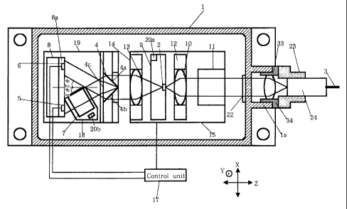
Fig. 1 is a plan cross-sectional view of an optical module constructed
according
to a first embodiment of the present invention;
Fig. 2 is a side cross-sectional view of the optical module shown in Fig. 1;
Figs. 3A-C are perspective views illustrating a procedure of assembling a
prism, optical filter and PD carrier used in the optical module shown in Figs.
1 and 2;
Figs. 4A-C are perspective views illustrating another procedure of assembling
the prism, optical filter and PD carrier used in the optical module shown in
Figs. 1 and
2;
Fig. 5 is a side cross-sectional view of an optical module constructed
according
to the second embodiment of the present invention;
Fig. 6A is a plan view of an optical filter used in an optical module
according
to the third embodiment of the present invention and Fig. 6B illustrates a
rotation of the
optical filter;
Fig. 7 is a side view of the optical filter shown in Fig. 6, in which Fig. 7A
shows the optical filter rotatably supported on a base and Fig. 7B shows the
optical filter
fixedly mounted on the base;
5
CA 02374841 2002-03-06
Figs. 8A and B are side and plan cross-sectional views of a holder member
used in an optical filter according to the fourth embodiment of the present
invention;
Fig. 9A is a plane view showing the holder member of Fig. 8 before it is
fixedly mounted on the base while Fig. 9B is a plan view showing the same
holder
member after it has fixedly been mounted on the base;
Figs. l0A and B are side cross-sectional and plan views showing the state of
the holder member of Fig. 8 when the optical filter is been angularly adjusted
by an
angle adjusting tool;
Fig. 11A is a plan view illustrating the structure and function of a prism
used in
an optical module according to the fifth embodiment of the present invention
while Fig.
11B is a perspective view of the prism;
Figs. 12A-D show several modified prisms;
Figs. 13A-D schematically illustrate a process of making an optical module
according to the sixth embodiment of the present invention;
Figs. 14A and B schematically illustrate the process of making the optical
module according to the sixth embodiment of the present invention;
Figs. 15A and B schematically illustrate the process of making the optical
module according to the sixth embodiment of the present invention;
Figs. 16A and B schematically illustrate the process of making the optical
module according to the sixth embodiment of the present invention;
Fig. 17 is a plan cross-sectional view of an optical module according to the
seventh embodiment of the present invention;
Fig. 18 is a plan cross-sectional view of an optical module according to the
eighth embodiment of the present invention;
Fig. 19 is a perspective view of another structure of PD carrier; and
Fig. 20 shows the structure of an optical module according to the prior art
and
having a wavelength monitor mounted therein.
DESCRIPTION OF THE IlWENTION
Several embodiments of the present invention will now be described with
reference to the drawings.
Fig. 1 is a plan cross-sectional view of an optical module constructed
according
6
CA 02374841 2002-03-06
to the first embodiment of the present invention; Fig. 2 is a side cross-
sectional view of
the optical module shown in Fig. 1; and Figs. 3 and 4 are perspective views
illustrating a
procedure of assembling a prism, optical filter and PD carrier which are used
in the
optical module according to the first embodiment of the present invention.
Referring now to Figs. 1 and 2, the optical module includes a hermetically
sealed package 1; a semiconductor laser element (or light-emitting device) 2
located
within the package 1 and for outputting a laser beam; an optical fiber 3 for
receiving and
externally delivering a laser beam outputted from the semiconductor laser
element 2 at
its front end face (right side as viewed in Fig. 1); a prism (or beam
splitter) 4 for
dividing a monitoring laser beam outputted from the semiconductor laser
element 2 at
its back end face (left side as viewed in Fig. 1) into two laser beam
components that are
inclined relative to the optical axis with the respectively predetermined
angles A 1 and
02, each of which is less than 90 degrees; a first photodiode (or photo
detector) 5 for
receiving one of the laser beam components divided by the prism 4; a second
photodiode (or photo detector) 6 for receiving the other laser beam component
from the
prism 4; an optical filter 7 disposed between the first photodiode 5 and the
prism 4 and
for permitting only a laser beam having a predetermined wavelength range to
transmit
therethrough; and a PD carrier (or mount member) 8 on which the first and
second
photodiodes 5, 6 are mounted in the same plane (which will be referred to the
same
mounting plane 8a).
The semiconductor laser element 2 is fixedly mounted on an LD carrier 9 on
which a thermistor 20a for sensing the temperature in the semiconductor laser
element 2
is located.
Between the semiconductor laser element 2 and the optical fiber 3 are disposed
a collimating lens (or first lens) 10 for collimating the laser beam outputted
from the
front end face of the semiconductor laser element 2 and an optical isolator 11
for
blocking any light reflected back by the optical fiber 3. The collimating lens
10 is held
by a first lens holder 12.
Between the semiconductor laser element 2 and the prism 4 is disposed another
collimating lens 13 for collimating the monitoring laser beam outputted from
the back
end face of the semiconductor laser element 2. The collimating lens 13 is held
by a
second lens holder 14.
7
CA 02374841 2002-03-06
The LD carrier 9, optical isolator 11, first lens holder 12 and second lens
holder
14 are fixedly mounted on a first base 15 that is in turn fixedly mounted on a
first
cooling device 16 including a Peltier module for cooling the semiconductor
laser
element 2 (see Fig. 2).
PD currents outputted from the first and second photodiodes 5, 6 are received
by a control unit 17 that, based on the received PD currents, controls the
temperature in
the first cooling device 16 to control the wavelength of the laser beam
outputted from
the semiconductor laser element 2.
The prism 4 includes two sloped light entering faces 4a, 4b formed into an
inverted V-shaped configuration and a flat light exiting face 4c. The laser
beam
outputted from the semiconductor laser element 2 is divided by the prism 4
into two
laser beam components as the laser beam enters both the two sloped faces 4a
and 4b of
the prism 4.
The whole surface of the prism 4 is coated with an AR (anti-reflection) film
for
suppressing the reflection of laser beam in the prism 4. The inclined angles8l
and 62 of
the laser beam components divided by the prism 4 are preferably substantially
equal to
each other (e.g., within a range between 15 and 45 degrees). This is because
the light
receiving positions of the first and second photodiodes 5, 6 will more easily
be
determined by use of such inclined angles.
The optical filter 7 may be made of etalon or the like and is fixedly mounted
on
a filter holder 18 of substantially L-shaped cross-section at its bottom and
side plates
18a, 18b through low temperature glass (i.e., glass with a low melting point)
or solder
(see Fig. 3B). The optical filter 7 can be moved by the filter holder 18 to
regulate the
angle of incident laser beam. The bottom or side plate 18a or 18b may support
a
temperature sensor such as a thermistor 20b. The thermistor 20b can accurately
measure
the temperature in the optical filter 7 since the bottom or side plate 18a or
18b is fixedly
mounted on the optical filter 7 through a good heat conducting bonding agent
such as
low temperature glass or solder and is positioned intimately close to the
optical filter 7.
The mounting surface 8a of the PD carrier 8 on which the first and second
photodiodes 5, 6 are mounted is inclined relative to the direction of incident
laser beam
with an angle 63 exceeding 90 degrees (see Fig. 2). The inclined angle 63 of
the
mounting surface 8a is preferably equal to or larger than 95 degrees for
reducing the
8
CA 02374841 2002-03-06
reflected-back light and for providing an improved characteristic. If the
mounting
surface 8a is inclined relative to the direction of incident laser beam with
an angle larger
than the aforementioned range of angle, PD currents capable of coupled with
the
photodiodes will not sufficiently be obtained. It is thus preferred that the
inclined angle
03 is at least smaller than 135 degrees for suppressing the degradation in the
coupling
efficiency within 3 dB. It is thus preferred that the inclined angle 63 in the
mounting
surface 8a is larger than 95 degrees but smaller than 135 degrees.
The prism 4, filter holder 18 and PD carrier 8 are fixedly mounted on a second
base 19. As shown in Figs. 3 and 4, the prism 4 is mounted in abutment with
the wall of
a first protrusion 19a formed on the second base 19 while the PD carrier 8 is
mounted
on a second protrusion 19b formed on the second base 19. The filter holder 18
is
mounted in a recess 19c formed on the second base 19 between the first and
second
protrusions 19a, 19b.
The thermistor 20b for sensing the temperature in the optical filter 7 may
fixedly be mounted on protrusions 19d that are formed on the second base 19 at
its
opposite sides.
As shown in Fig. 2, the second base 19 is fixedly mounted on a second cooling
device 21 that includes a Peltier module. The second cooling device 21 is
controlled to
maintain the temperature sensed by the thermistor 20b (20) constant. A
separate control
unit may be used for performing the control operation, or control unit 17 may
be used.
The package 1 includes a flange portion 1 a formed therein on one end. The
flange portion 1 a houses a window 22 on which the light passed through the
optical
isolator 11 is incident and a condensing lens (or second lens) 33 for
condensing the laser
beam onto the end face of the optical fiber 3. The condensing lens 33 is held
by a third
lens holder 34 that is fixedly mounted on the outer end of the flange portion
1 a through
YAG laser welding. A metallic slide ring 23 is fixedly mounted on the outer
end of the
third lens holder 34 through YAG laser welding.
=== The ferrule 24 holding the tip end of the optical fiber 3 is fixed in the
interior of
the slide ring 23 through YAG laser welding at a predetermined position.
The top of the package 1 is closed by a lid 25 (see Fig. 2), the outer
periphery
of which is resistant-welded to the package 1 to hermetically seal it.
The laser beam outputted from the front end face of the semiconductor laser
9
CA 02374841 2002-03-06
element 2 is collimated by the collimating lens 10 and then enters the
condensing lens
33 through the optical isolator 11 and window 22. After condensed by the
condensing
lens 33, the laser beam is received and externally delivered by the optical
fiber 3 held by
a ferrule 24.
On the other hand, the monitoring laser beam outputted from the back end face
of the semiconductor laser element 2 is collimated by the collimating lens 13
and
divided by the prism 4 into two laser beam components having their inclined
angles A 1
and 62 relative to the optical axis.
One of the laser beam components divided by the prism 4 is received by the
optical filter 7 through which only a laser beam having a predetermined
wavelength
range transmits. The transmitted light is received by the first photodiode 5.
The other
laser beam component is received by the second photodiode 6. PD currents
outputted
from the first and second photodiodes 5, 6 is received by the control unit 7
that, based
on a differential voltage (or voltage ratio) between the two received PD
currents,
controls the temperature sensed by the thennistor 20a of the first cooling
device 16 to
maintain the wavelength of the beam outputted from the semiconductor laser
element 2
constant.
The prism 4, optical filter 7, first photodiode 5, second photodiode 6 and PD
carrier 8 for fixedly supporting them forms a wavelength monitor unit for
monitoring
the wavelength of the laser beam, together with the collimating lens 13 and
second base
19, if necessary.
A process of making the optical module according to the first embodiment of
the present invention will be described below.
First of all, the LD carrier on which the semiconductor laser element 2 is
mounted, the optical isolator 11, the first lens holder 12 and the second lens
holder 14
are fixedly mounted on the first base 15 through soldering.
Thereafter, the first base 15 is soldered onto the first cooling device 16
that has
already been mounted in the package 1. Similarly, the second base 19 having no
matter
mounted on the top thereof is fixedly mounted on the second cooling device 21
that has
already been mounted in the package 1.
Next, the prism 4 is properly positioned relative to the X-axis direction such
that the monitoring laser beam outputted from the back end face of the
semiconductor
CA 02374841 2002-03-06
laser element 2 will enter the two sloped faces 4a and 4c of the prism 4.
Subsequently,
the prism 4 is brought into abutment with the first protrusion 19a of the
second base 19
and fixedly positioned thereat through low temperature glass or solder (see
Fig. 3A).
Next, the PD carrier 8 is positioned and fixedly soldered on the second
protrusion 19b of the second base 19 such that the laser beam components
divided by
the prism 4 will enter both the first and second photodiodes 5, 6 (see Fig.
3C). The
thermistor 20b is then fixedly soldered onto the bottom or side plate 18a or
18b in the
filter holder 18.
Next, the optical filter 7 fixedly mounted on the filter holder 18 (see Fig.
3B) is
placed (or roughly set) in the recess 19c of the second base 19 between the
prism 4 and
the first photodiode 5 (see Fig. 4A).
Next, the wavelength characteristic is measured based on the PD current from
the first photodiode 5 produced in response to receiving the light passed
through the
optical filter 7 while moving the optical filter 7 to change the angle of
incident laser
beam (see Fig. 4B).
Next, the optical filter 7 is fixedly mounted on the second base 19 at such a
position that is judged to provide the desired wavelength characteristic from
the
measurements, through YAG laser welding . This position is referred to as the
wavelength locking point.
Next, the position of the optical fiber 3 is regulated relative to X-, Y- and
Z-
axes such that the output of the laser beam from the front end face of the
semiconductor
laser element 2 will be maximized. The femile 24 holding the tip end of the
optical fiber
3 is fixed in the interior of the slide ring 23 through YAG laser welding at a
position.
Thereafter, the slide ring 23 is fixedly mounted on the end face of the flange
portion 1 a
formed on the package 1 on one side through YAG laser welding.
Finally, the opened top of the package 1 is closed by the lid 25, the outer
periphery of which is YAG laser welded to the package 1 to hermetically seal
it.
According to the first embodiment of the present invention, the first and
second
photodiodes 5, 6 for receiving the laser beam components divided by the prism
4 are
mounted on the single PD carrier 8 in the same mounting surface 8a. Thus, the
number
of parts can be reduced to lower the manufacturing cost. Since the two
photodiodes 5
and 6 can optically be aligned with only a single PD carrier 8, the number of
11
CA 02374841 2002-03-06
manufacturing steps can be reduced to shorten the manufacturing time.
Since the laser beam from the semiconductor laser element 2 is optically
coupled with the prism 4 through the collimating lens 13 and divided by the
prism 4 into
two laser beam components received by the two photodiodes 5 and 6 on the
single PD
carrier 8, the optical paths can be reduced in length, thus making the
necessary space
compact. Thus, the optical module can be reduced in size with an improved
coupling
efficiency on conducting the monitoring laser beam to the photodiodes 5 and 6.
Since the position of the optical filter 7 is regulated relating to its angle
in the
final step, after the other components in the wavelength monitor unit have
been
incorporated into the optical module, and since the wavelength characteristic
of the
optical filter 7 is regulated while viewing the PD outputs, the optical module
including
its wavelength monitor is iYnproved in wavelength regulation accuracy and can
be
produced with yield improvement.
Since the incident beam is divided by the roof prism 4, and since the division
at
the prism 4 can be carried out even though the angle of incident beam onto the
prism 4
is smaller than 90 relative to the optical axis of the incident light, the
loss for the
polarization dependency can be reduced. This will be described in more detail
in
connection with Fig. 11. Since the prism 4 is not a large-sized optical part
such as a
dividing coupler, the optical module including the wavelength monitor
according to the
present invention can be reduced in size. When the roof prism 4 is used in
such a
manner, the angle of light to be divided can be regulated depending on the
angle
between the two sloped face of the roof prism. Therefore, the size of the
optical module
can further be reduced.
Since the laser beam entered two or more faces in the prism 4 is divided into
beams transmitted through the prism 4, the wavelength dependency between the
divided
laser beam components can be reduced. Particularly, where the laser beam is
divided
into laser beam components having the same inclined angle relative to the
optical axis in
the incident light, the same wavelength dependency is provided between the
divided
laser beam components. In the arrangement of this embodiment in which the
divided
laser beam components are compared with each other, the wavelength dependency
of
the laser beam created from the division can be canceled.
Since the temperature in the optical filter 7 is maintained constant by the
12
CA 02374841 2002-03-06
thermistor 20b disposed intimately close to the optical filter 7 and the
second cooling
device 21, the wavelength characteristic of the optical filter 7 can be
stabilized to
maintain the wavelength of the laser beam outputted from the semiconductor
laser
element 2 constant with improved accuracy.
Fig. 5 is a side cross-sectional view of an optical module according to the
second embodiment of the present invention. As shown in Fig. 5, the second
embodiment provides a base member 26 of an integral structure combining the
first and
second bases 15, 19 and a cooling unit 27 of an integral structure combining
the first
and second cooling devices 16, 21. According to the second embodiment, the
number of
necessary parts can further be reduced and the manufacturing process can
further be
simplified.
Fig. 6A is a plan view of an optical filter used in an optical module
according
to the third embodiment of the present invention while Fig. 6B illustrates the
rotation of
the optical filter. Fig. 7 is a side view of the optical filter shown in Fig.
6: Fig. 7A shows
the optical filter rotatably supported on a base and Fig. 7B shows the optical
filter
fixedly mounted on the base.
Referring to Figs. 6A and B, the optical filter 7 used in an optical module
according to the third embodiment of the present invention is characterized by
that it is
fixedly mounted on a disc-shaped filter holder 28 that is rotatable about a
rotation axis L
perpendicular to the direction of incident laser beam. This rotation axis L is
one that
passes through the intersection between the diagonal lines in the square
optical filter 7,
as shown in Fig. 6B.
As shown in Fig. 7A, the optical filter 7 is fixedly mounted, at its bottom,
on a
filter holder 28 through low temperature glass or adhesive. The bottom of the
optical
filter 7 may be soldered to the filter holder 28 after it has been metallized.
The
underside of the filter holder 28 includes a cylindrical anchoring base 28a
extending
therefrom, which base 28a is inserted into a circular hole A formed in the
base 19 (or
26) for rotation relative to the base 19 (or 26). After the angle in the
optical filter 7 has
been regulated while monitoring PD currents, the anchoring base 28a is fixed
to the
base 19 (or 26) at a position in which the desired wavelength characteristic
of the
optical filter 7 is provided, through YAG laser welding, as shown in Fig. 7B.
A
thermosetting adhesive may be charged into a gap between the anchoring base
28a and
13
CA 02374841 2002-03-06
the base 19 (or 26) and heated to set such a thermosetting adhesive after the
angle of the
optical filter 7 has been regulated.
In such a manner, the filter holder 28 is supported on the base 19 (or 26) for
rotational movement about the rotation axis L perpendicular to the direction
of incident
laser beam. Therefore, the optical filter 7 can more easily be aligned.
Figs. 8A and B are side and plan cross-sectional views of a holder member
used in an optical filter according to the fourth embodiment of the present
invention;
Fig. 9A is a plane view showing the holder member of Fig. 8 before it is
fixedly
mounted on the base while Fig. 9B is a plan view showing the same holder
member
after it has fixedly been mounted on the base; Figs. l0A and B are side cross-
sectional
and plan views showing the state of the holder member of Fig. 8 when the
optical filter
is been angularly adjusted by an angle adjusting tool.
Referring to Fig. 8, the optical module according to the fourth embodiment of
the present invention includes a prism 4, optical filter 7 and PD carrier 8,
all of which
are fixedly mounted in a holder member 29 consisting of a hollow metal block.
The optical filter 7 is mounted on a filter holder 30 that is fixedly mounted
on
the holder member 29 in such a manner as shown in connection with the third
embodiment. The filter holder 30 is a part independently of the holder member
29 and
can rotatably be aligned about a rotation axis L2 perpendicular to the
direction of
incident laser beam to regulate the angle of incident light onto the optical
filter 7. The
filter holder 30 is rotatably supported between the top and bottom of the
holder member
29.
Referring to Fig. 9A, the base 19 (26) is formed with a groove portion 31 such
that the holder member 29 can be aligned in such a state that the laser beam
is not
emitted from the semiconductor laser element 2, that is, in a passive
alignment. The
holder member 29 is inserted while meeting the side face thereof to the groove
portion
31. This can simplify the aligning step. After the holder member 29 has been
inserted
into the groove portion 31 in the base 19 (26), a YAG laser beam is irradiated
to the
contacting area therebetween to perform the welding, as shown in Fig. 9B. Fig.
9B
shows six YAG welding spots represented by black circles. The laser welding
may be
replaced by the soldering or adhesive.
As shown in Fig. 10A, the top face of the filter holder 30 is externally
exposed
14
CA 02374841 2002-03-06
through the top of the holder member 29. As shown in Fig. lOB, for example,
the
exposed top may be formed with a fitting groove 30a into which the tip portion
32a of
an angle regulating too132 is engaged, the angle regulating tool 32 being then
rotated to
regulate the angle in the optical filter 7. This facilitates the regulation of
angle in the
optical filter 7. Moreover, the exposed top of the filter holder 30 may be
formed with a
protrusion that is adapted to engage into a fitting groove in the angle
regulating too132.
In addition, the filter holder 30 may magnetically be rotated to regulate the
angle in the
optical filter 7 when the tip face of the angle regulating too132 is in
contact with the top
of the filter holder 30. In any event, the angle in the optical filter 7 can
easily be
regulated in the limited space within the package 1.
Fig. 11A is a plan view illustrating the structure and function of a prism
used in
an optical module according to the fifth embodiment of the present invention
while Fig.
11B is a perspective view of the prism.
Referring to Figs. 11A and B, the fifth embodiment uses a roof type prism 4
having a pentagonal configuration as viewed in a plane, the prism having two
sloped
faces 4a and 4b that receive an incident light and divides it into two light
portions. The
prism 4 is symmetrical about the axis M. The sloped (or light entering) faces
4a and 4b
in the prism 4 are coated with an AR film having no polarizing property or the
like. The
arrangement is made such that the incident light collimated by the collimating
lens 13
enters the ridgeline 4d and adjacent area of the prism 4 including the sloped
faces 4a
and 4b.
When the light enters the area adjacent to the ridgeline 4d, an angle 64
included between each of the sloped faces 4a, 4b in the prism 4 and the normal
in the
incident light (as shown by R in Fig. 11A) becomes the angle of incident light
in the
prism 4. This angle of incidence 64 is preferably as small as possible for
reducing the
loss in the polarization dependency. When the angle of incidence 64 is equal
to or
smaller than 65 degrees, the loss in the polarization dependency can
effectively be
reduced. Practically, the angle of incidence 84 is determined, for example,
between 10
degrees and 65 degrees, depending on the dimensions of the photodiodes 5, 6
and prism
4 that are used in the measurement.
Figs. 12A-D show several modified prisms. Although Fig.. 11 shows the roof
prism 4, the latter may be formed into such shapes as shown in Fig. 12A. The
prism 4
CA 02374841 2002-03-06
shown in Fig. 12A divides the light incident thereon near the vertex T into
three light
portions while the prism 4 shown in Fig. 12B divides the light incident
thereon near the
vertex T into four light portions. The prism 4 may be of a roof configuration
asymmetrical relative to the axis M, as shown in Fig. 12C.
In such a roof prism 4 as shown in Fig. 12D, a flat face 4c thereof opposite
to
the incident faces may receive the light and divide it into two light
portions.
Considering the reflection of the light from the incident faces of the prism 4
toward the
semiconductor laser element 2, however, it is preferred that the sloped faces
3a and 3b
form the incident faces as shown in Figs. 1 and 11.
Figs. 13-16 schematically illustrate a process of making an optical module
according to the sixth embodiment of the present invention.
Referring first to Fig. 13A, the LD carrier 9 on which the semiconductor laser
element 2 has been mounted and the PD carrier 8 on which the photodiodes 5 and
6
have been mounted are positioned on the base 26 in place through the passive
alignment
and fixedly soldered thereto. The soldering material used may be AuSn or the
like.
As shown in Fig. 13B, the laser beam is then emitted from the front end face
of
the semiconductor laser element 2. By using the emitted laser beam, the first
lens holder
12 for holding the collimating lens 10 is aligned relative to X-Y-Z-6 axis
directions
through an aligning tool 35. After aligned, the fnst lens holder 12 is fixed
to the base 26
in place through YAG laser welding.
As shown in Fig. 13C, the optical isolator 11 is aligned relative to the X-Y-Z-
6
axis directions through an aligning tool 36 and fixed to the base 26 in place
through
YAG laser welding. Such a step may be omitted if the optical isolator 11 is to
be not
mounted on the base 26.
As shown in Fig. 13D, the second lens holder 14 for holding the collimating
lens 13 is then aligned relative to the X-Y-Z-6 axis directions through an
aligning tool
37 without emitting the laser beam from the back end face of the semiconductor
laser
element 2 or in the passive alignment and fixed to the base 26 in place
through YAG
laser welding.
As shown in Fig. 14A, the base 26 is then fixedly soldered on the cooling
device 27.
Next, the semiconductor laser element 2, the photodiodes 5 and 6 are
16
CA 02374841 2002-03-06
electrically connected to leads (not shown) in the package 1 through gold
wires (not
shown)
Next, as shown in Fig. 14B, the prism 4 is aligned relative to the X-Y-Z-6
axis
directions through an aligning tool 38 to provide the desired current values
while
monitoring the PD currents outputted from the photodiodes 5 and 6. The aligned
prism
4 is then fixed onto the base 26 in place through YAG laser welding.
Next, as shown in Fig. 15A, the optical filter 7 is aligned relative to the X-
Y-Z-
9 axis directions through an aligning tool 39 to provide the desired
wavelength
characteristic (or wavelength discriminating curve) while monitoring the PD
currents
outputted from the photodiodes 5 and 6. Once aligned, the optical filter 7 is
fixed onto
the base 26 through YAG laser welding.
Next, the thermistors 20a and 20b are electrically connected to leads (not
shown) in the package 1 through gold wires (not shown).
Next, as shown in Fig. 15B, the lid portion 25 is placed over the opened top
of
the package 1 within the atrnosphere of inert gas (e.g., N2 or Xe), the outer
periphery
thereof being then resistance-welded to the package to hermetically seal it.
Next, as shown in Fig. 16A, the third lens holder 34 for holding the
condensing
lens 33 is placed. within the flange portion la of the package 1 and aligned
relative to
the flange portion 1 a in the X-Y plane and in the Z-axis direction. The third
lens holder
34 is fixed in the flange portion 1 a through YAG laser welding such that the
light rays
exiting from the condensing lens 33 are made parallel to the center axis of
the flange
portion 1 a in the package 1.
Finally, the optical fiber 3 is aligned and fixed. In this step, the metallic
slide
ring 23 is fixedly mounted on the outer end of the third lens holder 34. The
slide ring 23
is fixed onto the outer end of the third lens holder 34 at the boundary
therebetween
through YAG laser welding after the slide ring 23 has been positioned in the
plane
perpendicular to the optical axis of the optical fiber 3 (X-Y plane). The
ferrule 24
holding the optical fiber 3 is fixed in the interior of the slide ring 23
through YAG laser
welding at a position wherein the outgoing beam in the optical fiber 3 is
maximized.
Thus, the optical axis direction (Z-axis direction) in the optical fiber 3 is
fixedly
positioned.
In such an embodiment, the semiconductor laser element 2, one PD carrier 8 on
17
CA 02374841 2002-03-06
which the first and second photodiodes 5, 6 and lenses are fixedly mounted and
lenses
are initially positioned in such a state that the laser beam is not emitted
from the
semiconductor laser element 2 (not depending on the amount of light and the
optical-
axis measurement), that is, according to the passive alignment. Thereafter,
the laser
beam is emitted from the semiconductor laser element 2 and the prism 4 is
aligned and
positioned relating to the position and angle thereof, based on the current
values
detected by the first and second photodiodes 5, 6 in such a typical manner
that the two
current values are substantially equal to each other, that is, according to
the active
alignment.
According to such a procedure, the semiconductor laser element 2, one PD
carrier on which the first and second photodiodes 5, 6 and lenses can more
easily be
positioned through the passive alignment. Additionally, the alignment of the
prism can
absorb variations in the optical axis and amount of PD entering light
associated with
variations in arrangement of these optical parts. Thus, the light can surely
enter the first
and second photodiodes 5, 6. And yet, the currents detected by the first and
second
photodiodes 5, 6 can also be regulated with the desired balance.
Therefore, the sixth embodiment can further reduce the manufacturing cost and
time of the optical module, than the first embodiment. The sixth embodiment
can also
produce the optical module having its improved wavelength stability for laser
beam in a
stable manner.
Fig. 17 is a plan cross-sectional view of an optical module according to the
seventh embodiment of the present invention.
The optical parts used in the aforementioned embodiments, such as the optical
filter 7, prism 4 and others, have the temperature dependencies in the optical
characteristics thereof. Thus, these parts are controlled for their
temperatures to be
maintained constant through the second or first cooling device 21 or 16.
However, they
are always influenced by changes in the external temperature outside of the
module.
Thus, the control of temperature in the second cooling device 21 may not
follow the
variations of temperature in the optical parts. If the temperature in such
optical parts and
particularly the optical filter 7 is variable, the output values of the two PD
currents are
correspondingly variable. This may more or less change the wavelength of the
laser
beam outputted form the semiconductor laser element 2.
18
CA 02374841 2002-03-06
To avoid such a problem, the seventh embodiment is provided with a correction
unit H that includes a circuit for receiving a temperature detection signal
outputted from
a thermistor 20b located adjacent to or on the filter holder 18 as shown in
Fig. 3 and for
outputting a temperature correction signal toward the control unit 17, as
shown in Fig.
17. The other components are substantially similar to those of the optical
module
according to the first embodiment. The temperature correction signal outputted
from
this correction unit H is used to correct the temperature controlled by the
first cooling
device 16 such that the wavelength in the laser beam outputted from the
semiconductor
laser element 2 will be maintained constant. Thus, the wavelength in the laser
beam
outputted from the semiconductor laser element 2 can be maintained constant
with very
high accuracy.
Fig. 18 is a plan cross-sectional view of an optical module according to the
eighth embodiment of the present invention. In the eighth embodiment, a
temperature
correction thermistor 40 may be located near the optical filter 7 and
connected with the
correction unit H, separately of the thermistor 20b.
In the eighth embodiment, the thermistor 20b is shown as to be formed on a
protrusion 19d of the second base 19 (see Fig. 3).
The present invention is not limited to the aforementioned forms, but may be
carried out in any of various modified or changed forms within the technical
scope as
defined in the appending claims. For example, the optical filter 7 may be
disposed
between the prism 4 and the second photodiode 6. Furthermore, the prism 4 is
designed
to divide the incident laser beam into two beam components that are inclined
with
different angles relative to the optical axis.
Additionally, the first and second photodiodes 5, 6 may respectively be
mounted on separate mount surfaces as shown in Fig. 19. From the viewpoint of
facilitating the optical alignment, it is preferred that these photodiodes are
mounted on
the same plane.
Additionally, the output strength in the laser beam outputted from the
semiconductor laser element 2 may be controlled based on the output (PD
current) from
the second photodiode 6.
The control unit aspects of this invention may be conveniently implemented
using a conventional general purpose digital computer, digital signal
processor or
19
CA 02374841 2002-03-06
microprocessor programmed according to the teachings of the present
specification, as
will be apparent to those skilled in the computer art. Appropriate software
coding can
readily be prepared by skilled programmers based on the teachings of the
present
disclosure, as will be apparent to those slcilled in the software art. The
invention may
also be implemented by the preparation of application specific integrated
circuits or by
interconnecting an appropriate network of conventional component circuits, as
will be
readily apparent to those skilled in the art.
The present invention includes a computer program product that is a storage
medium including instructions that can be used to program a computer to
perform a
process of the invention. The storage medium can include, but is not limited
to
semiconductor memory including ROMs, RAMs, EPROMs, EEPROMs, magnetic
memory including floppy disks or hard disks, and optical media such as optical
disks,
all of which are suitable for storing electronic instructions.
Obviously, additional numerous modifications and variations of the present
invention are possible in light of the above teachings. It is therefore to be
understood
that within the scope of the appended claims, the present invention may be
practiced
otherwise than as specifically described herein.