Note: Descriptions are shown in the official language in which they were submitted.
CA 02375153 2001-11-23
WO 00/78013 PCT/US00/15992
Loop Driver For POTS, XDSL, Or Integrated POTS/XDSL Interface
The present invention relates to the field of voice and data communications
system and more particularly to interface circuits for coupling a combination
of telephony
and high-rate data communications functions to a 2-wire telephone loop.
BACKGROUND OF THE INVENTION
With the increasing popularity of the Internet, there has been a corresponding
requirement for high rate digital transmission over the local subscriber loops
of telephone
companies. A loop is a twisted-pair copper telephone line. Loops can differ in
distance,
diameter, age, and transmission characteristics, depending on the network.
These loops
are a natural conduit for provision of high speed digital communications
services due to
the large installation base that already exists. Digital transmission systems
on these loops
include asymmetric, symmetric, high-rate, and very high-rate digital
subscriber loops,
conventionally known as ADSL, SDSL, HDSL, and VDSL respectively. Normally
these
and other similar protocols are known as xDSL.
Of these flavours of xDSL, ADSL is intended to co-exist with traditional voice
services by using different frequency spectra on the loop. In the future, it
is possible that
multiple different transmission schemes may be employed in different frequency
bands
on the same loop, and that these transmission schemes may include traditional
analog
voice services as well as current and new forms of xDSL. In today's ADSL
system, the
plain old telephone services (POTS) uses the frequency spectrum between 0 and
4kHz
and the ADSL uses the frequency spectrum between 30kHz and 1.lMHz for data
over the
telephone line. This is shown schematically in figure la. ADSL also partitions
its
frequency spectrum with upstream (subscriber to CO) transmission in a lower
frequency
band, typically 30kHz to 138kHz, and with downstream transmission in a higher
frequency band , typically 138kHz to SSOkHz or l.lMHz. ADSL uses a discrete
multi-
tone (DMT) multi-carrier technique that divides the available bandwidth into
approximately 4kHz sub-channels.
The architecture, interfaces and protocols for telecommunications networks
incorporating ADSL modems is shown in figure 1b. The elements consist of one
of more
ATU-C's 2 or ADSL modems at a central office end 4. The ATU-C 2 can be
integrated
within an access node 6 which is the concentration point for broadband data 8
and
CA 02375153 2001-11-23
WO 00/78013 PCT/US00/15992
narrowband data 10. Broadband and narrowband in this context is meant
switching
systems for data rates above lMbps and switching systems for data rates at or
below
lMbps respectively. The access node 6 can be located at a central office, or a
remote site.
Also a remote access node can subtend from a central access node. The ATU-C's
2 are
coupled via a sputter 12 to the telephone loop 14. The loop 14 at the customer
end is also
coupled via a sputter 12 to the telephone loop 14. The loop 14 at the customer
end is also
coupled via a sputter 12 to an ATU-R 16 or an ADSL modem at the customer end
that
can be integrated within an SM (Service Module) which are devices that perform
terminal-adaptation functions. Examples are set top boxes, PC interfaces, or
LAN
routers. The PSTN (Public Switched Telephone Network) 18 to the subscriber
phones 20
shares the loop 14 via the sputter 12 which isolate the POTS form the ADSL
modems.
As shown in figure 2, an analog sputter 24 provides the filtering required to
separate the POTS and ADSL bands before being input to their respective
transceivers.
Generally, the sputter 34 consists of a low pass filter 36 between the
telephone and the
loop and a highpass filter between the ADSL transceiver and the loop. The low
frequency components output form the LPF are sent to the conventional
telephone line
card. These analog signals are converted to digital signals and encoded as PCM
signals
by and A/D CODEC. These signals may then be combined with other PCM signals
and
transmitted to other central offices or switching networks. The sputter is
generally a very
bulky and expensive component. A number of solutions have been proposed to
eliminate
the sputter. For example, US Patent No. 5,757,803 describes an improved
sputter, while
US Patent No. 5,889,856 describes an integrated ADSL line card with a digital
splitter.
It is generally assumed that the function of the POTS sputter is only to
separate
the different frequency bands and send them to their respective transceiver.
The actual
function is more complex and deals with the need to provide the correct
impedance in
different frequency bands in order to allow the signals to properly propagate
and meet the
relevant specifications. While the conventional POTS sputter does eliminate or
reduce
the effects of interference from the POTS and ADSL equipment, a properly
designed
interface may eliminate these problems with adding the low or high pass
filters in the
signal path.
Matching a line interface card to the loop is relatively less complicated in a
narrow frequency band. Various circuits for achieving such a matching are
described
U.S. Patent 5,515,433. However, these circuits are limited when a broadband
matching is
required. The present invention thus seeks to mitigate some of the above
disadvantages.
2
CA 02375153 2001-11-23
WO 00/78013 PCT/US00/15992
SUMMARY OF THE INVENTION
The invention seeks to provide a solution to the general problem of requiring
a
POTS sputter in an integrated line interface module and, in particular, at the
central office
or "head end". An advantage of the present invention is that it may be used
for a
combined telephony and digital subscriber loop ("DSL") service or other
communications
systems where the telephony and data, or different types of data, occupy
different
frequency spectra on a 2-wire communication line.
A further advantage of the invention is to eliminate the traditional POTS
sputter
and to provide a broadband loop driver and termination that allows frequency
dependent
impedance synthesis to be implemented using highly integrated circuits using
either
digital, analog or a combination of digital and analog means. A further
advantage of the
invention is to minimize power, cost and size for delivering integrated voice
and data.
In accordance with this invention there is provided a drive circuit comprising
a
transformer having a primary winding for coupling to a subscriber loop and a
secondary
winding for coupling to an interface circuit; a feedback circuit for coupling
the primary
winding to the secondary winding to provide a predetermined impedance match
between
the interface circuit and the loop over a predetermined frequency band of the
circuit.
BRIEF DESCRIPTION OF THE DRAWINGS
These and other features of the preferred embodiments of the invention will
become more apparent in the following detailed description in which reference
is made to
the appended drawings wherein:
Figure 1(a) is a diagram showing the frequency spectrum of an ADSL system;
Figure 1(b) is a schematic diagram of an ADSL system architecture;
Figure 2 is a schematic diagram of a prior art ADSL modem;
Figure 3 is a schematic diagram of a prior art DSL transceiver;
Figure 4 is a schematic diagram of an ADSL modem according to an embodiment
of the present invention;
Figure 5 is a schematic block diagram of the an ADSL modem according to an
embodiment of the present invention;
Figures 7(a)-(f) are schematic diagrams of drive circuits according to
embodiments of the present invention; and
3
CA 02375153 2001-11-23
WO 00/78013 PCT/US00/15992
Figures 8 (a)-(~ are detailed schematic circuit diagrams of the circuits in
figures
7(a)-(f).
DESCRIPTION OF THE PREFERRED EMBODIMENTS
In the following description, like numeral refer to like structures in the
drawings.
Refernng to figure 2, a DSL central office system, according to the prior art,
is
shown generally by numeral 20. The system comprises an ADSL transceiver 21 for
processing digital data, a POTS sputter 34, and a POTS transceiver
incorporating a SLIC
(subscriber line interface circuit) 26 and a CODEC 22 for processing voice
data. The
POTS splitter 24 is coupled to a subscriber loop 28 which then splits off the
voice signal
and provides it to the SLIC and CODEC 22 and a high frequency data signal to
the ADSL
transceiver 21. The ADSL transceiver includes a DSL baseband circuit 31
coupled to the
broadband data path, a DSL analog front-end (AFE) 33 which is fed from the DSL
baseband circuit couples to the sputter 24 via a loop driver. The ADSL
transceiver
provides bi-directional communication between the broadband data path and the
loop.
The digital processing circuits provide for the digital signal processing
function such a
modulation, echo cancellation and equalization. Typically the AFE includes
both
transmit and receive channels. The transmitter channel consists of a digital
to analog
converter (D/A) coupled to the broadband data bus, transmit filters, followed
by a line
driver coupled through a hybrid to the sputter. The receive channel includes a
receive
filter coupled to the hybrid, a programmable gain amplifier driving an analog
to digital
converter, which in turn outputs digital signal to the digital processing unit
onto the
broadband data path. Both the transmit and receive channels are couple to the
sputter
which is in turn coupled by a transformer to the loop.
As described in the background of the invention, there are many disadvantages
with this arrangement.
The present invention involves modification to this conventional arrangement
by
integrating the voice/data analog front end (AFE) 42 and the voice/data
baseband 44 with
a common loop driver 46 as shown schematically in figure 4. The integrated
unit thus
provides bi-directional communication between the loop and a system bus or
busses
carrying ADSL and PCM data. If this integrated approach is taken, the
frequency
dependent termination in each frequency band must be synthesized by the AFE
42, the
baseband 44, or a combination of the two. Further, the loop driver must
provide
4
CA 02375153 2001-11-23
WO 00/78013 PCT/US00/15992
relatively flat response over the full range of frequency bands, which in an
integrated
POTS and ADSL application would be from 200Hz to 1.lMHz.
Referring to figure 5, a top level block diagram of an integrated line
interface
module 40 of figure 4, for voice and data requirements according to an
embodiment of the
S present invention is shown in greater detail. The AFE 42 includes a loop
driver 52
coupled to the loop, a wide band AFE 54 possibly including impedance synthesis
and
coupled to the loop driver 52, and A/D and D/A converters 56. The AFE thus
provides
bi-directional communication between the loop and the digital processing
section 44 and
may provide full or partial frequency dependent impedance synthesis.
The digital processing section 44 may include a digital impedance synthesis
unit
58 which is coupled to the AFE 42. The unit performs either full or partial
impedance
synthesis required for the composite system and provides frequency dependent
filtering
and equalization. The composite signal is coupled to a baseband processing
unit
comprising one or more DSP based processing elements which implement the voice
CODEC 60 and ADSL modem 62 functions. The baseband processing unit is coupled
to
one or more system busses carrying a high speed ADSL data and PCM voice
signals.
A feature of this architecture is a broadband loop drive circuit which allows
the
integration of the complex impedance synthesis function in highly integrated
digital or
analog circuit. In a preferred embodiment, the loop driver provides DC feed
capability of
up to 100mA; flat or nearly flat frequency response between 200Hz and 1.lMHz
or
beyond; balanced loop drive; AC signal swing of up to 22V peak; and low power
dissipation.
One approach in the prior art is to utilize a broadband SLIC implemented in a
high
voltage integrated circuit technology. In this approach, the SLIC needs to
carry both DC
loop currents, low frequency voice signals, and high frequency data signals.
This
approach suffers from a variety of problems including excessive power
dissipation
because of the large signal currents and signal voltage headroom required on
the driver
amplifiers; difficulty of implementation in silicon technologies; and limited
loop range
with 48V battery feed.
A preferred approach is to use a transformer based drive circuit for coupling
the
integrated voice/xDSL unit to the loop. The primary difficulties in using a
transformer-
based solution are caused by transformer roll-off at low and high frequencies
because of a
combination of primary inductance, leakage inductance and interwinding
capacitance and
core limitations.
5
CA 02375153 2001-11-23
WO 00/78013 PCT/US00/15992
Referring to figures 7(a)-(f), various transformer based drive circuits for
coupling
the integrated voice/xDSL unit to the loop are shown. All seek to avoid the
problems
caused by transformer limitations by using feedback techniques to linearize
the
performance of the circuits in this application.
In figure 7(b) a transformer configuration is shown having a feedback loop for
overdriving the input. In figure 7(c) a pair of transformers is provided, with
a high
frequency feed forward on the second transformer. Figure 7(d) is a variation
of the
configuration of figure 7(c) wherein a high frequency feed forward with a
capacitor is
provided. Finally in figure 7(e) two transformers are provided with a separate
drive to the
second transformer.
In figure 8(a) - 8(f) a broadband transformer has a split primary with the
first
winding and a second winding having polarities in the manner shown. The
transformer
has a single secondary winding 104. As used herein, the primary refers to the
loop side of
the line feed transformer and the secondary refers to the voice/xDSL modem
side of the
transformer. The transformer's primary to secondary turns ratio is preferably
about 1:1
but can be other ratios. Typically, the line transformer is a 1:1 which must
maintain a
magnetizing inductance of 100mH to 2H while carrying 20mA to 100mA in the
primary
winding. The typical AC voltage swing is up to 22 volts peak, while the
impedance
looking onto the loop is in the order of 900 ohms in the voice band and 100
ohms in the
ADSL band.
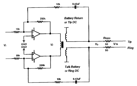
Referring to figure 8(a) and an interface circuit (not shown) provides an
input V;
to a driver circuit 180 which is coupled to a twisted pair telephone loop
having TIP and
RING leads which generally extend between the central office and customer
premises.
The drive circuit includes a transformer having a pair of primary windings
coupled to the
respective TIP and RING lines by a respective line feed elements Rfeea which
are typically
50 ohms. The other ends of the primary windings are connected to respective
battery
return or TIP DC and a talk battery or RING DC. On the secondary side of the
transformer, the input voltage V; is provided to each terminal of the
secondary via
respective inverting opamps.
In figure 8(a) the first primary winding 106 is coupled at one end to a feed
resistor 107 coupled one of the loop conductors TIP, while the second primary
winding
108 is coupled to a feed resistor 110 coupled to the second of the loop
conductors RING.
In figure 8(b) the differential voltage at the primary side is sensed and fed
back to
the secondary side. The feedback circuit senses the differential output
voltage Vo on the
6
CA 02375153 2001-11-23
WO 00/78013 PCT/US00/15992
primary side of the transformer, compares that differential output voltage Vo
to the
desired output voltage Vi, and multiplies the error signal by a high gain to
generate a
feedback signal Vf and drives the secondary of the with the signal Vf to
provide increased
drive to the transformer.
In figure 8(c) the differential voltage at the primary side is sensed and fed
back to
the secondary side. The feedback circuit senses the differential output
voltage Vo on the
primary side of the transformer, compares that differential output voltage Vo
to the
desired output voltage Vi, and multiplies the error signal by a high gain to
generate a
feedback signal Vf and drives the primary side of the transformer with Vf
through
capacitors. The secondary side of the transformer is driven by the desired
input voltage
Vi.
In figure 8(d) the differential voltage at the primary side is sensed and fed
back to
the secondary side. The feedback circuit senses the differential output
voltage Vo on the
primary side of the transformer, compares that differential output voltage Vo
to the
desired output voltage V;, and multiplies the error signal by a high gain to
generate a
feedback signal Vf and drives the primary side of the transformer with
complimentary
signals Vt~ through respective capacitors. The secondary side of the
transformer also
driven by the feedback signal Vf.
In figure 8(e) the differential voltage at the primary side is sensed and fed
back to
the secondary side. The feedback circuit senses the differential output
voltage Vo on the
primary side of the transformer, compares that differential output voltage Vo
to the
desired output voltage Vi, and multiplies the error signal by a high gain to
generate a
feedback signal Vf and drives the primary side of the transformer a second
transformer
coupled through capacitors. The signal Vf drives the secondary of the second
transformer
2~ and the primary windings of the second transformer are capacitively coupled
to the output
voltage Vo. The secondary side of the first transformer is driven by the
desired input
signal Vi.
In figure 8(f) the differential voltage at the primary side is sensed and fed
back to
the secondary side. The feedback circuit senses the differential output
voltage Vo on the
primary side of the transformer, compares that differential output voltage Vo
to the
desired output voltage Vi, and multiplies the error signal by a high gain to
generate a
feedback signal Vf and drives the primary side of the transformer a second
transformer
coupled through capacitors. The signal Vf drives the secondary of the second
transformer
7
CA 02375153 2001-11-23
WO 00/78013 PCT/US00/15992
and the primary windings of the second transformer are capacitively coupled to
the output
voltage Vo. The secondary side of the first transformer driven by the output
signal V~
Figure 8(g) is similar to figure 8(f) except that an impedance is also added
between the primary windings of the first transformer and the output voltage
Vo. In this
configuration, the two transformers can be configured to provide drive in
different
frequency bands, with the crossover frequency determined by the impedances in
series
with the two transformers.
Although the invention has been described with reference to certain specific
embodiments, various modifications thereof will be apparent to those skilled
in the art
without departing from the spirit and scope of the invention as outlined in
the claims
appended hereto.
8