Note: Descriptions are shown in the official language in which they were submitted.
CA 02375291 2002-03-08
GENERATION OF VIRTUAL LOCAL OSCILLATOR INPUTS FOR USE IN DIRECT
CONVERSION RADIO SYSTEMS
BACKGROUND OF THE INVENTION
The present invention relates generally to communications, and more
specifically to up-conversion and down-conversion, being a frequency
generation device providing waveforms for use in a Virtual Local Oscillator-
base system.
Many communication systems up-convert electromagnetic signals from
baseband to higher frequencies for transmission, and subsequently down-
convert those high frequencies back to their original frequency band when
they reach the receiver, processes known as up-conversion and down-
conversion (or modulation and demodulation) respectively. The original (or
baseband) signal, may be, for example, data, voice or video. These baseband
signals may be produced by transducers such as microphones or video
cameras, be computer generated, or transferred from an electronic storage
device. In general, the high frequencies provide longer range and higher
capacity channels than baseband signals, and because high frequency radio
frequency (RF) signals can propagate through the air, they can be used for
wireless transmissions as well as hard wired or fibre channels.
All of these signals are generally referred to as radio frequency (RF)
signals, which are electromagnetic signals; that is, waveforms with electrical
and magnetic properties within the electromagnetic spectrum normally
associated with radio wave propagation.
Wired communication systems which employ such modulation and
demodulation techniques include computer communication systems such as
local area networks (LANs), point to point signalling, and wide area networks
(WANs) such as the Internet. These networks generally communication data
signals over electrically conductive or optical fibre channels. Wireless
CA 02375291 2002-03-08
2
communication systems which may employ modulation and demodulation
include those for public broadcasting such as AM and FM radio, and UHF and
VHF television. Private communication systems may include cellular
telephone networks, personal paging devices, HF (high frequency) radio
systems used by taxi services, microwave backbone networks, interconnected
appliances under the Bluetooth standard, and satellite communications. Other
wired and wireless systems which use RF up-conversion and down-
conversion would be known to those skilled in the art.
For cellular telephones, for example, it is desirable to have transmitters
and receivers (which may be referred to in combination as a transceiver)
which can be fully integrated onto inexpensive, low power, integrated circuits
(ICs).
As frequencies of interest in the wireless telecommunications industry
(especially low-power cellular/micro-cellular voice/data personal
communications systems) have risen above those used previously
(approximately 900 MHz) into the 1 GHz -5 GHz spectrum, the desire to
implement low-cost, power efficient receivers and transmitters has led to
intensive research into the use of highly integrated designs, an increasingly
important aspect for portable systems, including cellular telephone handsets.
Several attempts at completely integrated transceiver designs have met
with limited success. Other RF receiver topologies exist, such as image
rejection architectures, which can be completely integrated on a chip, but
lack
in overall performance. Although many receivers use the "super-heterodyne"
topology, which provides excellent performance, this does not meet the
desired level of integration for modern wireless systems.
Direct conversion architectures demodulate RF signals to baseband in a
single step, by mixing the RF signal with a local oscillator signal at the
carrier
frequency of the RF signal. There is therefore no image frequency, and no
image components to corrupt the signal. Direct conversion receivers offer a
high level of integratability, but also have several important problems.
Hence,
CA 02375291 2002-03-08
3
direct conversion receivers have thus far proved useful only for signalling
formats that do not place appreciable signal energy near DC after conversion
to baseband.
A typical direct conversion or homodyne receiver is shown in Figure 1. The
RF band pass filter (BPF1 ) 102 first filters the signal coming from the
antenna
100 (this band pass filter 102 may also be a duplexer). A low noise amplifier
104 is then used to amplify the filtered antenna signal, increasing the
strength
of the RF signal and reducing the noise figure of the receiver.
The signal is then split into its quadrature components and down-
converted to baseband in a single stage using mixers MI 110 and MQ 120,
and orthogonal signals generated by local oscillator (LO) 132 and 90 degree
phase shifter 130. LO 132 generates a regular, periodic signal which is tuned
to the carrier frequency of the incoming wanted signal rather than a frequency
offset from the carrier as in the case of the super-heterodyne receiver. The
signals coming from the outputs of MI 110 and MQ 120 are now at baseband,
that is, having a carrier frequency of 0 Hz. The two signals are next filtered
using low pass filters LPFI 112 and LPFQ 122, are amplified by
gain-controlled amplifiers AGCI 114 and AGCQ 124, and are digitized via
analog to digital converters ADI 116 and ADQ 126.
Direct conversion RF receivers as illustrated in Figure 1 have several
advantages over super-heterodyne systems in terms of cost, power
consumption, and level of integration, however, there are also several serious
problems with direct conversion. These problems include:
~ noise near baseband (that is, 1/f noise) which corrupts the desired
signal. The term "1/f noise" is used to describe a number of types of noise
that
are greater in magnitude at lower frequencies than at higher frequencies
(typically, their magnitude increases roughly with the inverse of the signal
frequency);
CA 02375291 2004-10-26
4
~ local oscillator (LO) leakage in the RF path that creates DC offsets in the
down-converted (base-band) output signal. As the LO frequency is the same
as the incoming signal being demodulated, any leakage of the LO signal
through the mixers 110, 120 to their RF port will fall directly into the
desired
signal's band and be down-converted to baseband as well;
~ local oscillator (LO) leakage into the RF path that causes
desensitization. Desensitization is the reduction of desired signal gain as a
result of receiver reaction to an undesired signal. The gain reduction is
generally due to overload of some portion of the receiver, such as the AGC
circuitry 114, 124 resulting in suppression of the desired signal because the
receiver will no longer respond linearly to incremental changes in input
voltage.
~ noise inherent to mixed-signal integrated circuits corrupts the desired
signal; and
~ large on-chip capacitors used as high-pass filters are required to remove
unwanted noise and signal energy near DC, which makes integratability
expensive. These capacitors are typically placed between the mixers 110, 120
and the low pass filters 112, 122.
What is needed is a simpler and more satisfactory means of generating
the signals required for certain Local Oscillator implementations.
BRIEF SUMMARY OF THE INVENTION
The invention provides a simplified and effective system and method for
generating a number of inputs to the mixer elements of a direct conversion
(homodyne) receiver configuration which uses certain Local Oscillator
techniques.
CA 02375291 2002-03-08
In this regard, Virtual Local Oscillators are used to provide the equivalent
of a local oscillator without using frequency generators having significant
spectral components (power) in the input frequency or intermediate
frequencies of the receiver circuit, thereby mitigating some of the
5 disadvantages listed above. Our co-pending PCT application (W00117122:
Improved Method and Apparatus for Up- and Down-Conversion of Radio
Frequency (RF) Signals, LING, YANG (CA); WONG, LAWRENCE (CA);
MANKU, TAJINDER (CA).) describes preferred implementations and relevant
sections are included in the detailed description for ease of reference.
In the implementation of a system using a Virtual Local Oscillator, the
circuit that generates the various time-varying signals or waveforms required
to operate the VLO invention presents significant design challenges. Designs
have been produced which are sufficient to serve the purpose, but they tend
to be complex and have higher power consumption.
The circuit that generates the various time-varying signals or waveforms
are required to have a fixed and stable phase-relationship, as well as being
correctly related in terms of their power spectra relative to the operating
radio
(RF), intermediate (IF), and baseband frequencies of the system. Such
waveforms, when applied to the mixer, permit the mixer to create internally
the effect of applying the Local Oscillator signal at the required frequency.
BRIEF DESCRIPTION OF DRAWINGS
Preferred embodiments will be described with reference to the following
figures.
Figure 1 represents a typical receiver architecture of a direct conversion or
homodyne receiver as known in prior art.
Figures 2A and 2B illustrate the Virtual Local Oscillator concept for which
the invention is suited.
CA 02375291 2002-03-08
6
Figure 3 is a diagram of a preferred embodiment of the invention.
Figure 4 illustrates the various time-varying signals or waveforms
produced from the circuit of Figure 3.
Figure 5 is a diagram of a further preferred embodiment of the invention.
DETAILED DESCRIPTION OF THE INVENTION
Since it is helpful to have some understanding of the concepts of a Virtual
Local Oscillator system, we have for completeness, incorporated a brief
description of the Virtual Local Oscillator, the subject of a co-pending PCT
application (W00117122: Improved Method and Apparatus for Up- and Down
Conversion of Radio Frequency (RF) Signals, LING, YANG (CA); WONG,
LAWRENCE (CA); MANKU, TAJINDER (CA)).
The Virtual Local Oscillator is concerned with the generation of signals
used in the conversion process which have properties that solve the image-
rejection problems associated with heterodyne receivers and transmitters and
the LO-leakage and 1/f noise problems associated with direct conversion
receivers and transmitters.
A circuit which addresses the problems outlined above, is presented as a
block diagram in Figure 2A. This figure presents a balanced modulator or
demodulator 270 in which an input signal x(t) is mixed with two synthesized
signals (labelled ~1 and ~2) which are irregular and vary in the time domain,
to effect the desired modulation or demodulation. The two mixers M1 272 and
M2 274 are standard mixers known in the art, having the typical properties of
an associated noise figure, linearity response, and conversion gain. The
selection and design of these mixers would follow the standards known in the
art, and could be, for example, double balanced mixers. Although this figure
implies various elements are implemented in analogue form they can be
implemented in digital form.
CA 02375291 2002-03-08
7
The two synthesizers 276 and 278 generate two time-varying functions ~1
and ~2 that mixed together within the mixer circuit comprise a virtual local
oscillator (VLO) signal. These two functions have the properties that their
product emulates a local oscillator (LO) signal that has significant power at
the
carrier frequency, but neither of the two signals has a significant level of
power at the frequency of the LO being emulated. As a result, the desired
modulation or demodulation is affected, but there is no LO signal to leak into
the RF path.
The representation in Figure 2A is exemplary, as any two-stage or multiple
stage mixing architecture may be used to implement the invention. As well,
the synthesizer for generating the time-varying mixer signals ~1 and ~2 may
comprise a single device, or multiple devices.
In current receiver and transmitter technology, frequency translation of an
RF signal to and from baseband is performed by multiplying the input signal
by regular, periodic, sinusoids. If one multiplication is performed, the
architecture is said to be a direct-conversion or homodyne architecture, while
if more than one multiplication is performed the architecture is said to be a
heterodyne or super-heterodyne architecture. Direct-conversion transceivers
suffer from LO leakage and 1/f noise problems which limit their capabilities,
while heterodyne transceivers require image-rejection techniques which are
difficult to implement on-chip with high levels of performance.
The problems of image-rejection, LO leakage and 1/f noise in highly
integrated transceivers can be overcome by using more complex signals than
simple, regular, periodic, sinusoids in the frequency translation process.
These signals have tolerable amounts of power at the RF band frequencies
both in the signals themselves and in any other signals produced during their
generation.
The preferred criteria for selecting such functions ~1 and ~2 are:
CA 02375291 2002-03-08
(i) for the signal x(t) to be translated to baseband, ~1 (t) * ~2(t) must have
a
frequency component at the carrier frequency of x(t);
(ii) in order to minimize spurious response problems, ~1 (t) * ~2(t) must
have less than a tolerable amount energy at frequencies other than the carrier
frequency of x(t) or at least far enough away that these image frequencies can
be significantly filtered on-chip prior to down-conversion;
(iii) in order to minimize LO leakage problems, the signals ø~1 and ~p2 must
not have significant amounts of power in the RF output signal bandwidth.
That is, the amount of power generated at the output frequency should not
effect the overall system performance of the transmitter or receiver in a
significant manner;
(iv) also to avoid LO leakage found in conventional direct conversion and
directly modulated topologies, the signals required to generate ~p1 and ~2, or
the intermediate signals which occur, should not have a significant amount of
power at the output frequency;
(v) ~2 * ~2 (sometimes written simply ~2~2) should not have a significant
amount of power within the bandwidth of the up-converted RF (output) signal.
This ensures that if ~1 leaks into the input port, it does not produce a
signal
within the RF signal at the output. It also ensures that if ~2 leaks into node
between the two mixers, it does not produce a signal within the RF signal at
the output; and
(vi) if x(t) is an RF signal, ~1 * ~1 * ~2 should not have a significant
amount of power within the bandwidth of the RF signal at baseband. This
ensures that if ~1 leaks into the input port, it does not produce a signal
within
the baseband signal at the output.
These signals can, in general, be random, pseudo-random, or periodic
functions of time, and may be either analogue, or digital time-varying signals
or waveforms.
CA 02375291 2004-10-26
9
It would be clear to one skilled in the art that virtual LO signals may be
generated which provide the benefits of the invention to greater or lesser
degrees. While it is possible in certain circumstances to have almost no LO
leakage, it may be acceptable in other circumstances to incorporate virtual LO
signals which still allow a degree of LO leakage.
An exemplary set of acceptable waveforms is presented in Figure 2B,
plotted in amplitude versus time. Five cycles of the VLO signal are presented,
labelled cp1cp2. It is important to note that at no point in the operation of
the
circuit is an actual cp1 cp2 signal ever generated; the mixers receive
separate
cp1 and cp2 signals, and mix them with the input signal using different
physical
components. Hence, there is no LO signal which may leak into the circuit. The
states of these cp1 and cp2 signals with respect to the hypothetical cp1cp2
output
are as follows:
1 2 1 2
C cle 1 - H I LO
LO
C cle 1 - LO LO
HI
C cle 2 - HI LO
LO
C cle 2 - LO LO
HI
C cle 3 - LO HI
LO
C cle 3 - LO LO
H1
G cle 4 - HI LO
LO
C cfe 4 - LO LO
HI
C cle 5 - LO H I
LO
Cycle 5 - HI HI
HI
While these signals in certain cycles may be described as "aperiodic",
groups of the cycles may be repeated successively. For example, the pattern
of the cp1 and cp2 input signals presented in Figure 2B which generate the
cp1cp2 signal, repeat with every five cycles. Longer cycles could certainly be
used.
It would be clear to one skilled in the art that many additional pairings of
signals may also be generated. The more thoroughly the above criteria (i) -
(vi) for selection of the cp1 and cp2 signals are complied with, the more
effective the invention will be in overcoming the problems in the art.
CA 02375291 2002-03-08
The topology of the virtual local oscillator is similar to that of other two
stage or multistage modulators and demodulators, but the use of irregular,
time-varying mixer signal provides fundamental advantages over known
transmitters and receivers, including:
5 ~ minimal 1/f noise;
~ minimal imaging problems;
~ minimal leakage of a local oscillator (LO) signal into the RF output band;
~ removes the necessity of having a second LO and various (often
external) filters; and
10 ~ has a higher level of integration as the components it does require are
easily placed on an integrated circuit. For example, no large capacitors or
sophisticated filters are required.
Since the mixers in most transceivers act as solid state switches being
turning on and off, it is preferable to drive the mixers using square time-
varying signals or waveforms rather than sinusoids. Square time-varying
signals or waveforms with steep leading and trailing edges will switch the
state of the mixers more quickly, and at a more precise moment in time than
sinusoid waveforms.
Turning to figures 3, 4 and 5 we will now describe various preferred
embodiments of the invention.
Note that throughout the figures and descriptions, reference is made to
amplifier stages which are not balanced. Those skilled in the art would
recognise that this is a simplification to assist in the explanation of the
invention, and that the use of balanced amplifiers would be typical.
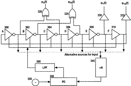
Preferred embodiments of the invention comprise a ring oscillator
operatively connected to a number of logical gates arranged to produced the
required time-varying signals. As shown in the Figure 3, a first preferred
CA 02375291 2004-10-26
11
embodiment of the invention comprises a series of five inverting amplifiers
300, 302, 304, 306, 308, followed by a non-inverting amplifier 310 connected
as a ring, the output of each of the first four inverting amplifiers 300, 302,
304,
306 being connected to the input of the next inverting amplifier, the output
of
the last inverting amplifier 308 being connected to the input of the non-
inverting amplifier 310 and the output of the non-inverting amplifier 310
being
connected to the input of the first inverting amplifier 300. The output of the
fifth
inverting amplifier 308 is also connected to a buffer amplifier 330 to produce
the time-varying signal cp,~ (t). The output of the non-inverting amplifier
310 is
also connected to another buffer amplifier 335 to produce the time-varying
signal cpz' (t). The outputs of the first inverting amplifier 300 and the
third
inverting amplifier 304 are connected to the two inputs of a first two-input
exclusive-OR gate 320 to produce a time-varying signal cp,Q (t) , and the
outputs of the second inverting amplifier 302 and the fourth inverting
amplifier
306 are connected to the two inputs of a second two-input exclusive-OR gate
325 to produce a time-varying signaIcpZQ (t). In this case, all of the time-
varying
signals cp,' (t), cp,Q (t), cp2' (t) and cpZQ (t) are square-waves and are
used as
inputs to various balanced mixers in the associated receiver circuit.
It will be appreciated that the input to the "divide-by-N" circuit 345 can
alternatively be fed by the output of any one of the amplifiers 300, 302, 304,
306 or 308 without substantially affecting the nature and performance of the
PLL subsystem.
Each of the five inverting amplifiers 300, 302, 304, 306, 308 and the non-
inverting amplifier 310 have a delay control input, all of which are connected
together and driven by the output of a low-pass filter 360. The input of the
low-
pass filter (LPF) 360 is driven by the output of a Phase Discriminator (PD)
350
(or phase comparison circuit) whose inputs are the output of a reference Local
Oscillator 355 and the output of a 'divide-by-N' (=N) circuit 345 driven by
the
output of the non-inverting amplifier 310, thereby forming a phase locked
loop.
CA 02375291 2004-10-26
11A
This Phase Locked Loop (PLL) circuitry provides frequency stability for the
ring oscillator by comparing the phase of the signal generated by the ring
oscillator with that provided by the local oscillator, in a manner
well-understood by those skilled in the art.
CA 02375291 2004-10-26
12
By appropriate selection of the outputs of the stages, and the application
of simple 'exclusive-OR' (XOR) logic gates, a number of time-varying signals
are generated which have the required stable relationships in frequency and
phase. Figure 4 shows the time-varying signals as generated by the circuit of
Figure 3 at various points in the circuit. Referring to both figures, the
outputs
of the buffer amplifiers 300, 302, 304, 306, 308, 310, are shown as A cp~Q(t)
400, B 402, C 404, D 406, E 408 and F cp~,(t) 410, and those of the XOR gates
320, 325, are shown as Bo-7D cp2,(t) 420 and C~E cp2Q(t) 430. The time-varying
signals labelled A cp~Q(t) 400, F cp"(t) 410, B~D cp2,(t) 420 and C~E cp2Q(t)
430
bear the necessary relationships to one another to be useful in a modulator or
demodulator taking advantage of the principles of a Virtual Local Oscillator.
The delay introduced by each of the buffer amplifiers 300, 302, 304, 306,
308, and 310 which comprise the Ring Oscillator is shown as 'd'. Variation of
this delay affects the actual oscillation frequency of the Ring Oscillator and
may be used as previously described in the provision of a phase locking
arrangement, but their relative differences will affect how closely the
signals
cp,Q(t) 400, F cp~,(t) 410, cp2,(t) 420 and cp2Q(t) 430 emulate the LO of a
direct
conversion receiver when used in the virtual local oscillator concept. These
differences can be minimized through the use of differential amplifier, so
that
the same amplifier can be used for all sections of the ring oscillator and
proper integrated circuit layout techniques to match the loading of each
amplifier stage. Buffers 330 and 335 are also used to match the delay of the
XORs 320 and 325.
Although the use of the phase locking loop arrangement is included here
because the inherent frequency stability of the ring oscillator may not be
sufficient for the VLO application, it is not a necessary element of the
invention. Other mechanisms may be used to provide the frequency stability
required by a particular application of the invention.
Other embodiments of the invention use different combinations of logic to
derive time-varying signals which have phase and frequency relationships
CA 02375291 2002-03-08
13
useful in the implementation of Virtual Local Oscillators for use in
modulation
and demodulation and like circuits or systems. Embodiments with more
stages within the ring of the ring oscillator may be used to derive a lesser
or
greater number of related time-varying signals using different logic elements
arranged to combine various outputs of the stages of the ring oscillator,
these
logic elements may include, but are not limited to, buffers, 'exclusive-OR'
(XOR), 'AND', and, 'OR' gates.
In a second preferred embodiment illustrated in Figure 5, seven inverting
amplifiers 500, 502, 504, 506, 508, 510, 512 and a non-inverting amplifier 514
form the ring oscillator, the outputs of the first 500, third 504 and fifth
508
amplifiers are combined through an XOR gate 520 to generate cp2,(t), and the
outputs of the second 502, fourth 506 and sixth 510 amplifiers are combined
through a second XOR gate 525 to generate cp2Q(t). The outputs of the
seventh 512 and eighth 514 stages are buffered 530, 535 to produce cp~Q(t)
and cp~,(t) respectively. The remaining elements, namely the low-pass filter
560, the Phase Discriminator 550, the reference Local Oscillator 555 and the
'divide-by-N' circuit 545 form the Phase Locked Loop (PLL) circuitry providing
frequency stability for the ring oscillator as before.
In further embodiments, I inverting amplifier stages (where I is an odd
integer, value five or more) and a single non-inverting amplifier stage
arranged as a ring oscillator may be used; the outputs of the odd-numbered
stages from 1 to (I - 2) are combined using an XOR gate to generate c~2,(t),
the
outputs of the even-numbered stages from 2 to (I - 1 ) are combined using a
second XOR gate to generate cp2Q(t), and the output of the Ith inverting
amplifier stage and the output of the non-inverting amplifier stage are
buffered
to generate cp,Q(t) and cp»(t) respectively.
In cases where balanced amplifiers are used more stages can be added to
the ring oscillator as long as there is an even number of stages in the
oscillator. Outputs of the odd stages must be combined to create the inphase
~ signals and outputs of the even stages must combined to create to the
CA 02375291 2002-03-08
14
quadrature g~ signals. More than two ~ signals may be generated for each of
the inphase and quadrature arms if all the ~ signals for each arm are added
modulo-2 to give a 50% duty cycle square-wave at the RF frequency. Any
logic elements can be used to generate the ~ signals as long as the delay
from all the ring oscillator outputs to the ~ outputs is matched well enough
that
spectrum of all the ~ signals added together modulo-2 has a large tone at the
RF frequency and does not contain significant power at frequencies other
than the RF frequency. In this context, "significant" means "large enough to
cause spurious response problems which degrade the overall receiver
performance to unacceptable levels".
A person skilled in that art will realise that the invention has application
elsewhere, and it is the intention of the inventor that this description
covers
those situations and applications insofar as they are not already known and in
use in the field. A person skilled in the art will realise that the
embodiments
described may be varied in detail without losing or detracting from the
inventive concept described herein, and it is our intention to encompass such
variations in design within the description and claims.