Note: Descriptions are shown in the official language in which they were submitted.
CA 02375326 2002-O1-15
WO 01/88557 PCT/USO1/15479
-1-
TITLE OF THE INVENTION
TEST PROBE AND CONNECTOR
CROSS REFERENCE TO RELATED APPLICATIONS
This application claims priority of U.S. Provisional
Application No. 60/205,045 titled Socketless Probe and
filed May 18, 2000.
STATEMENT REGARDING FEDERALLY SPONSORED RESEARCH OR
DEVELOPMENT
N/A
BACKGROUND OF THE INVENTION
The present invention relates to probes that are
used in printed circuit board test fixtures and more
particularly, to a socketless, leaktight replaceable
probe for use in a test fixture.
It is known to provide testing fixtures for printed
circuits boards (PCBs) and the like, for testing the
integrity of the electrical connectivity of the circuit
boards. A conventional embodiment of a testing apparatus
is shown in Fig. 1, and includes a fixed, stationary
substantially horizontal probe plate 10 and an overlying
vertically spaced movable top plate 12. Top plate 12 is
linked to probe plate 10 by means of a peripheral
elastomeric spacer 14 which allows top plate 12 to
vertically move towards probe plate 10 upon a vacuum
being created inside the sealed enclosure formed by probe
plate 10, spacer 14, top plate 12, and an overlying
pressure plate (not shown) sealingly engaging the upper
CA 02375326 2002-O1-15
WO 01/88557 PCT/USO1/15479
_2_
face of top plate 12. The downward movement of top plate
12 is accomplished by elastomeric spacer 14 partly
collapsing under the movable top plate 12 being sucked
downwards by the vacuum.
Top plate 12 holds on its upper surface a printed
circuit board 18 which is securely anchored thereto by
the above-mentioned pressure plate upon the vacuum being
created. Circuit board 18 is spaced from top plate 12 by
means of rigid spacers 20, 22 and is aligned, relative to
probe plate 10, by means of a number of alignment rods 16
which are fixedly attached to probe plate 10 and which
upwardly extend through and loosely engage respective
vertically registering channels 23 provided in top plate
12 to engage alignment holes provided in circuit board
18.
A number of tapered channels 24 extend transversely
through top plate 12, with a test probe 26 being located
under and vertically registering with each channel 24.
Each test probe 26 is fixedly attached to probe plate 10
in a manner described hereinafter, and vertically extends
above and below probe plate 10. Top plate channels 24
further vertically register with electrical contact
points 28 to be tested on printed circuit board 18 upon
engagement with the probe tip of the test probe 26. Thus,
upon top plate 12 moving downward, the probe tip of the
test probe 26 abuts the selected contact point 28 to be
tested on the printed circuit board 18. Through the
instrumentality of known software, electric current is
transmitted sequentially through selected probes to test
the integrity of the electrical connectivity of the
printed circuit board 18.
CA 02375326 2002-O1-15
WO 01/88557 PCT/USO1/15479
-3-
The probes 26 of known construction are removably
inserted in a sleeve (socket) 30 fixedly anchored to the
probe plate 10. Sleeve 30 in turn is connected to a
computer-controlled circuit which allows electrical
current to be selectively transmitted therethrough. Probe
26 includes a tube in which a plunger is vertically
movable under the bias of a spring, between a lower and
an upper limit position. The plunger, the tube and the
sleeve are all electrically connected to each other, for
allowing the electric current to be transmitted to the
printed circuit board. The movable plunger is
continuously biased upwardly, and is downwardly forced
against the bias of the spring when the printed circuit
board downwardly moves against the upper tips of the
probes when the vacuum is created inside the sealed
enclosure. The purpose of providing a probe which is
distinct from its holding sleeve is that the probe has a
limited life span, and will thus have to be changed after
a certain number of uses because of wear.
Three important problems exist with the above-
described conventional circuit board testing apparatus:
a) The first problem is that the stationary sleeves
holding the probes prevent the use of more sturdy probes
for any given probe spacing. In fact, the contact points
of the probes on the printed circuit boards are closely
adjacent to one another, and thus the probes need to be
positioned in a closely adjacent fashion. This is
becoming more and more important as the miniaturization
of the printed circuit boards evolves. Thus, if the
contact points of the probes on a printed circuit board
are very close to one another, probes of a smaller
CA 02375326 2002-O1-15
WO 01/88557 PCT/USO1/15479
-4-
diameter need to be used to allow the probes to be
positioned closer to each other. Since the sleeves
carrying the probes have a larger diameter than the
probes themselves, circuit board contact points which are
closer to one another require sleeves of smaller
diameter, and consequently probes of even smaller
diameter. Probes having a very small diameter are less
sturdy and more prone to accidental breakage.
b) The second problem is that the vertical alignment
of the probe tips with their respective registering
circuit board contact points is in practice not always
achieved. Indeed, when inserting the probes inside their
respective sleeves, a certain vertical angular offset may
occur. The top plate channels are tapered to promote
self-alignment of the probes therein; however, the probe
tips may still be slightly misaligned when they protrude
beyond their respective channels in the space between the
top plate and the printed circuit board. The consequence
of this misalignment is that the probe tips may be
allowed to contact the printed circuit board in a
slightly offset fashion relative to their intended
respective contact points, which may result in electric
current not being transmitted to the circuit board.
Thus, the testing software could falsely indicate a
connection error.
c) The third problem also relates to a possible
misalignment between the probe tips and their
corresponding intended circuit board contact points, due
to the fact that the alignment rods, which are used to
position the circuit board, are fixed to the probe plate.
Indeed, it is possible that a misalignment of the top
CA 02375326 2002-O1-15
WO 01/88557 PCT/USO1/15479
-5-
plate relative to the probe plate may result in the top
plate through-channels being laterally offset relative to
their corresponding underlying probes, since the circuit
board position is determined by the alignment roads which
are integrally attached to the probe plate, while the
position of the through-channels depends on the position
of the top plate. If the through-channels are laterally
offset relative to their corresponding probes, then
certain probes may be laterally deflected by the edges of
their corresponding through-channels when the top plate
is lowered, which may result in the tips of these
deflected probes abutting against the circuit board aside
from their intended position. Again, the testing software
would then detect a connection error on the printed
circuit board where there is none.
Reference is here also made to U.S. Patent No.
4,885,533 assigned to the assignee of the present
application which discloses a probe which, in use, is
firmly engaged in an electrically conductive socket
mounted tightly in a dielectric plate of a PCB testing
fixture.
BRIEF SUMMARY OF THE INVENTION
In accordance with the present invention an improved
probe and connector are disclosed that are adapted for
use in a printed circuit board test fixture. The probe
includes a conductive tubular housing or body and a
conductive plunger that is contained and movable within
the housing. The plunger includes a contact tip that
extends out one end of the housing. The plunger and tip
are urged to a normally outward position by a bias force
CA 02375326 2002-O1-15
WO 01/88557 PCT/USO1/15479
-6-
created by a coil spring disposed within the housing. At
the opposing end of the probe from the contact tip, the
probe end defines a bore that is suitable sized to
receive a cooperative pin located at one end of a
connector.
The connector includes a tubular body that may be
mounted in a through-hole within a fixture plate. The
connector may be fixedly retained within the fixture
plate via an annular barb or a plurality of annular beads
located on the tubular body. In a preferred embodiment,
the connector includes the connector pin at one end and a
terminal of a desired configuration at the opposing end.
The terminal may include a wire-wrap pin, a crimp type
terminal for crimp attachment to a wire, or a spring
loaded plunger for wireless conductive engagement with an
electrical contact such as is located on a printed
circuit board. The connector pin receiving end of the
probe may contain one or more detents for retaining in
the end to retain the probe on the connector once the
connector pin is disposed in assembled relation with the
probe bore.
Additionally, the connector includes a tapered
portion between the connector pin and the connector body.
The tapered portion increases in diameter from the
connector pin to the connector body so that an air tight
seal is created between the probe and the connector upon
seating of the pin receiving end of the probe over the
connector pin.
Other features, aspects and advantages of the
presently disclosed probe and connector will be apparent
CA 02375326 2002-O1-15
WO 01/88557 PCT/USO1/15479
from the Detailed Description of the Invention that
follows.
BRIEF DESCRIPTION OF THE SEVERAL VIEWS OF THE DRAWING
The invention will be more fully understood by
reference to the following Detailed Description of the
Invention in conjunction with the drawings, of which:
Fig. 1 is a schematic side elevation showing a prior
art circuit board testing fixture;
Fig. 2 is a schematic elevation showing a circuit
board testing fixture according to the present invention;
Fig. 3 is a cross-sectional side elevation of a
sleeveless testing probe according to the present
invention;
Fig. 4 is an under view of the probe of Fig. 3;
Fig. 5 is an elevation of one embodiment of
connector for connecting and supporting the probe of
Figs. 3;
Fig. 6 is a sectional elevation of an alternative
embodiment to the connector of Fig. 5;
Fig. 7 is an illustrative arrangement showing
various probe an connector implementations;
Fig. $ is a partial side view of the probe plunger
of Fig. 3 illustrating alternative embodiments of probe
tips that may be employed;
Fig. 9 is a schematic side elevation illustrating
one embodiment of a connector for use with the test probe
depicted in Fig. 3; and
Fig 10 is a schematic side elevation illustrating
another embodiment of a connector for use with the test
probe depicted in Fig. 3.
CA 02375326 2002-O1-15
WO 01/88557 PCT/USO1/15479
_g_
DETAILED DESCRIPTION OF THE INVENTION
The entire disclosure of U.S. Provisional
Application No. 601205,045 titled Socketless Probe and
filed May 18, 2000 is hereby incorporated by reference.
Fig. 2 depicts a circuit board testing fixture 40
with a probe and one embodiment of probe connector in
accordance with the present invention. A testing fixture
40 includes a movable dielectric top plate 42 provided
with a number of bores 44 which transversely extend
through the top plate 42. These will be detailed
hereinafter. Testing fixture 40 further comprises a
dielectric intermediate alignment plate 46 which is
spaced from top plate 42 by a peripheral elastomeric
spacer 48 of known construction. A dielectric lower probe
plate 52 is located spaced under intermediate plate 46 by
a rigid peripheral wall 54. A printed circuit board 58 to
be tested is installed so as to rest on the top surface
of top plate 42 and is properly positioned relative to
top plate 42 by means of alignment rods 60, 62 which
protrude from and are fixed to top plate 42 and which
engage holes (not shown) in printed circuit board 58. As
known in the art, a pressure plate 64 is positioned
spacedly over printed circuit board 58, plate 64 being
supported by a rigid peripheral wall 66 provided with an
underlying peripheral elastomeric pad . 70. Downwardly
projecting fingers 74, 76 are integrally carried by an
intermediate portion of pressure plate 64.
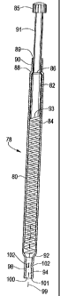
A number of testing probes 78 (only one testing
probe being shown in Fig. 2) are provided on testing
fixture 40. Referring to Figs. 3 and 4, each testing
CA 02375326 2002-O1-15
WO 01/88557 PCT/USO1/15479
_g_
probe 78 comprises a gold clad electrically conductive
hollow tube 80 which is engaged by a vertically slidable
gold-plated electrically conductive plunger 82
continuously upwardly biased by a coil spring 84. Plunger
82 has a gold-plated probe tip 85 and is provided at its
intermediate portion with an annular shoulder 86 which
abuts a complementary upper annular seat 88, adjacent the
upper end of tube 80, to prevent plunger 82 from moving
beyond an upper limit position under the bias of spring
84. Between the seat 88 and the open end 89 of the tube
80, through which the plunger 82 extends to the tip 85,
is a reduced diameter elongate retaining and sliding
bearing region 90 produced by swaging or rolling the tube
80 radially inwardly against a reduced diameter outer
portion 91 of the plunger 82 connecting the annular
shoulder 86 with the tip 85. This bearing region 90 has a
close clearance with the outer portion 91 to provide
excellent tolerance to side loading forces and smooth
long life reciprocal axial movement of the plunger 82
against the bias of the spring 84 with. no edges or
corners to contact, scrape and wear the plunger 82.
Additionally, the swaging or rolling of the tube 80
against the outer portion 91 of the plunger 82 produces
the desired clearance between the bearing region 90 and
the outer portion 91 as a result of material spring back
(hysteresis) following the swaging or rolling operation.
Tube 80 also has a lower annular spring seat 92
against which rests the lower end of spring 84. Plunger
82 preferably has an inclined lower surface 93 which is
engaged by the upper end of spring 84, to simultaneously
bias plunger 82 upwardly and radially against tube 80 to
CA 02375326 2002-O1-15
WO 01/88557 PCT/USO1/15479
-10-
ensure a reliable electrical connection between plunger
82 and tube 80. The lower end of tube 80 comprises an
axial bore 94 for sealed resilient connection between
tube 80 and a connector 96 (see Fig. 5) providing good
electric transmissibility and probe support.
Fig. 2 show that probe 78 is carried by a connector
96 fixedly anchored in probe plate 52, and more
particularly that connector 96 engages bore 94, as will
be detailed hereinafter. Moreover, probe 78, and more
particularly tube 80, extends through intermediate plate
46 in a registering guiding channel 81 provided therein.
A sealed enclosure is formed between lower probe
plate 52 and pressure plate 64, with channels 81 and 44
providing for fluid communication the areas between
plates 52, 46, 42 and 64. A vacuum port (not shown) is
provided in probe plate 52, to allow a vacuum to be
created in the sealed enclosure.
In use, a vacuum is created in the sealed enclosure,
wherein the elastomeric peripheral spacer 48 will
gradually collapse to allow top plate 42 to downwardly
move towards intermediate plate 46 for the probe tips 85
to come into contact with selected registering contact
points on printed circuit board 58; and wherein the
peripheral elastomeric pad 70 will also collapse to allow
pressure plate 64 to move towards top plate 42 whereby
the fingers 74, 76 of pressure plate 64 will abut against
and firmly support printed circuit board 58 against the
upward bias of the numerous probe plungers 82.
The guiding channels 81 provided in intermediate
plate 46 will correctly vertically align probes 78 so
that they register with the contact points on circuit
CA 02375326 2002-O1-15
WO 01/88557 PCT/USO1/15479
-11-
board 58 which they are intended to contact. Moreover,
the top plate throughbores 44 also promote proper self-
alignment of probes 78 relative to the corresponding
circuit board contact points. Indeed, the top plate bores
44 each have a lower portion 44a of increased diameter,
which allows the corresponding probe tip 85 to engage the
bore 44 even if the probe tip is slightly misaligned; a
tapered intermediate neck portion 44b, which allows the
probe tip orientation to be corrected if it is slightly
misaligned; and an elongate upper portion 44c which
extends up to the printed circuit board 58 and which has
a diameter to guide the corresponding probe tip 85 to the
circuit board contact point.
Additionally, the fact that circuit board 58 rests
directly on top plate 42 and is positioned thereon by
means of the alignment rods 60, 6~ which are fixedly
attached to the top plate 42, ensures that the contact
points of circuit board 58 which are intended to come
into contact with respective probe tips 85, will be
properly aligned relative to the top plate bores 44.
Thus, in view of these improvements over prior art
devices, misalignment of the probe tips 85 relative to
their corresponding intended circuit board contact points
is very unlikely, if not almost completely obviated.
Also, according to the invention, the testing probe
78 is not installed in a socket or sleeve, as with prior
art devices. Indeed, probe 78 engages a connector 96
directly, through the instrumentality of its axial bore
94. The intermediate plate guiding channel 81 allows
vertical alignment of the probe to be achieved even
CA 02375326 2002-O1-15
WO 01/88557 PCT/USO1/15479
-12-
though no elongate supporting socket or sleeve is
present.
The axial bore 94 is an elongate cylindrical bore
defined by a cylindrical tubular extension 98 of the tube
80 opposite the elongate bearing 90. The tubular
extension 98 extends from an annular shoulder forming the
spring seat 92 and is coaxial with the longitudinal axis
99 of the tube 80, spring 84 and plunger 82. The tubular
extension 98 defines a circular connector pin receiving
opening 100 which is itself defined by a smooth circular
inner edge 101.
The tubular extension 98, as with the bearing region
90, is integral with the remainder of the tube 80 and may
be formed by rolling or swaging.
At least one detent 102 is pressed or stamped
inwardly into the wall of the extension 98 intermediate
the length of the extension 98 between the shoulder for
the spring seat 92 and the opening 100. Preferably there
are three such detents 102 evenly spaced about the
circumference of the extension and in a plane normal to
the axis 99. The detents 102 do not perforate the tubular
extension 98.
Alternatively, the one or more detents can be
provided in a separate tube, rather than the extension of
the main tube.
Referring now to Fig. 5, a first embodiment of
connector 96 is described. The connector 96 is gold
plated, electrically conductive and includes a connector
pin 103 terminating in an annular curved tip, to
facilitate entry into probe bore 94 (Fig. 3) through
opening 100 and a parallel portion 104 to closely fit
CA 02375326 2002-O1-15
WO 01/88557 PCT/USO1/15479
-13-
within the probe bore 94 and to engage the detent(s) 102
to resiliently and firmly, but removably, support and
retain the probe 78 on the connector 96 in good
electrical contact therewith.
The inner end of pin 103 remote from the curved tip
terminates with an annular taper 105 sized to sealingly
engage the smooth circular edge 101 of the probe
extension opening 100 when the connector pin 103 is fully
engaged in the bore 94.
The connector pin 103 is connected to a wire-wrap
pin 109 by way of a plate connector portion 106 sized to
extend through plate 52 (Fig. 2) and to be fixedly
mounted in a circular opening extending through the plate
52. The fixed mounting is, as shown, by an interference
fit aided by an annular plate engaging ridge 107.
Alternative fixed mountings could be provided by splines
on the portion 106, the use of adhesives, molding-in,
etc.,. as would be well known to those skilled in this
technology.
A positive stop flange 108 is designed to control
the degree of insertion of the connector 96 into the
plate 52.
Typically, by way of example, for a probe having an
O.D. of 0.054 inch, the bore 94 has an I.D. of 0.0265
inch and the pin 103 has a parallel portion 104 with an
O.D. of 0.025~0.0003 inch, a taper 105 increasing from
the parallel portion 104 to a maximum O.D. of 0.028~0.001
inch with an included angle of 15~2 degrees. Probes of
these dimensions with sleeve mounting would require probe
spacing in a fixture of 0.100 inch, whereas with the
present invention a center spacing for the probes without
CA 02375326 2002-O1-15
WO 01/88557 PCT/USO1/15479
-14-
sleeves may be reduced to 0.075 inch. Similarly, center
to center reductions apply also to probes of other sites.
Fig. 6 illustrates a second embodiment of connector
97. In this embodiment features common with those of the
first embodiment of connector will not be described
again. The connector 97 is a two-part assembly for
connecting an insulated wire 110 to the probe 78 by way
of a gold plated electrically conducting pin 111
externally similar to pin 103 but hollow to receive the
electrical conductor 112 of the wire 110 which is crimped
at 113 in the hollow interior of the pin 111 to provide
good electrical interconnection. A polyester (nylon)
sleeve 114 is attached to the pin 111 by an annular
protrusion 115 on an extension of the pin 111. The
sleeve 114 covers the junction of the pin 111 and the
insulation 116 of the wire 110 and provides for the fixed
engagement of the connector 97 in a circular opening in
plate 52.
The connectors) 96, 97 are sealingly engaged with
the plate 52 to provide an air tight mounting such that
air and any contaminants cannot be drawn through the
fixture or the body of the probe when a vacuum is applied
during a testing phase.
Fig. 7 illustrates a variety of probe arrangements
providing differing probe heights achieved by varying the
length of protruding outer portions 91 of the plungers 82
and/or the axial length of the stop flange 108 of the
connectors 96 (or 97). Additionally, this figure shows
two connectors 117, the ends 118 of which include
wireless terminations for engaging a printed circuit test
board. An exemplary connector that provides a wireless
CA 02375326 2002-O1-15
WO 01/88557 PCT/USO1/15479
-15-
termination is illustrated in greater detail in Fig. 10
and is discussed below.
The probe 78 may be provided with a probe tip of
configurations that differ from the probe tip 85 depicted
in Fig. 3. Referring to Fig. 8, exemplary alternative
probe tips are shown. For example, a spherical probe tip
130,, a spear probe tip 132 or a chisel probe tipe 134 may
be provided on the end of the plunger 91 intended to
contact the printed circuit board 58. Probe tips of other
configurations may also be used.
Referring to Fig. 9 an alternative embodiment of a
connector 140 having a wirewrap pin termination is
depicted installed in the lower probe plate 52. The
connector 140 includes a connector pin 142, a plate
connector portion 144 and an annular tapered portion 146
between the connector pin 142 and the plate connector
portion 144. Additionally, the connector 140 includes a
wire wrap pin 148 at the opposite end of the plate
connector portion 144 from the connector pin 142. Two
annular beads 150 are provided on the plate connector
portion 144. The diameter of the annular beads 150 is
specified to provide an interference fit with the
respective hole in the lower probe plate 52. Upon
insertion of the connector 140 within the respective hole
in the probe plate 52, the annular beads 150 secure the
connector within the probe plate 52 and maintain vertical
alignment of the connector 140 within the probe plate 52.
Referring to Fig. 10 a further embodiment of a
connector 160 that provides a wireless termination is
depicted both with a printed circuit board 162 present
beneath the connector 160 and absent beneath the
CA 02375326 2002-O1-15
WO 01/88557 PCT/USO1/15479
-16-
connector 160. The connector 160, in one embodiment, is
fabricated in first and second connector portions 164 and
166 respectively. The first portion 164 includes a
connector pin 168 for insertion within the axial bore 94
of the testing probe 78 (Fig. 3). Additionally, the first
portion includes a body 170 and the connector pin 168
extends from one end of the body 170. A tapered annulus
is provided between the connector pin 168 and the body
170 to provide a seal when the connector pin 168 is
disposed within the axial bore 94 as discussed
hereinabove. An axial bore 174 is provided in the end of
the first portion 164 opposite the connector pin 168 to
receive a cooperative mating pin 176 at one end of the
second portion 166 of the connector 160. The mating pin
176 extends from one end of a tube 178. A probe 180
having a probe tip 182 is disposed within the tube 178
and is urged outward via a coiled bias spring (not
shown). As shown in the connector 160 on the left in Fig.
10, the probe is disposed in an extended position the
absence of the printed circuit board. As shown in the
connector 160 on the right of Fig. 10, the probe tip 182
is urged into contact with the printed circuit board 162
so as to make an electrical connection with a contact
point located on the printed circuit board 162. The
first connector portion 164 includes two annular beads
184 for securing the first connector portion 164 within
the lower probe plate 52 and maintaining vertical
alignment of the connector 160 within the probe plate 52.
While the connector 160 is illustrated as being
fabricated in first and second portions 164 and 166, in
an alternative embodiment, a connector that permits
CA 02375326 2002-O1-15
WO 01/88557 PCT/USO1/15479
-17-
wireless termination may be fabricated as a component
that includes a tubular body portion having a connector
pin at one end that is sized for insertion within the
axial bore 94 of the testing probe 78. A probe is
disposed within the tubular body and includes a probe tip
that extends from the end of the body opposite the
connector pin. A plurality of annular beads may be
provided on the body to secure the connector within the
lower probe plate 52. In this manner, the electrical
connection between the mating pin 176 and the bore 174 of
the first connector portion 164 depicted in Fig. 10 is
eliminated.
An advantage of the presently described probe and
connector is that no sleeves or sockets are used for
holding and vertically aligning the probes. Indeed, the
probes are positioned on their corresponding connectors
which engage detents in the probe that resiliently and
releasably hold and support the probe. This prevents the
probes from being accidentally released e.g. during
assembly of the fixture. Moreover, the intermediate
plate allows the probes to be substantially vertically
aligned. The absence of the probe-carrying sockets or
sleeves allow the use of probes of larger diameters, for
a given required probe spacing, which will consequently
be more sturdy and less likely to be accidentally damaged
and which will resist wear longer than probes 'using
sleeves or sockets.
Also, the alignment of the probes with their
respective contact tips on the printed circuit board is
enhanced by the presence of the top plate throughbores
which extend from the probe tip up to the printed circuit
CA 02375326 2002-O1-15
WO 01/88557 PCT/USO1/15479
-18-
board, thus preventing the probe tip from being laterally
offset and to contact the printed circuit board elsewhere
than on its intended contact point thereon. The
intermediate plate throughbores, and the fact that the
alignment rods are fixed to the top plate instead of the
probe plate, also help improve alignment of the probes
with their respective intended contact points on the
printed circuit board.
It should be noted that the presently disclosed test
probes and connectors may be fabricated of any suitable
metal such as berylium copper and may be plated with gold
or other suitable material to enhance conductivity and/or
to reduce corrosion.
It will be appreciated by those of ordinary skill in
the art that modifications to and variations of the above
described socketless probe may be made without departing
from the inventive concepts described herein.
Accordingly, the invention should not be viewed as
limited except as by the scope and spirit of the appended
claims.