Note: Descriptions are shown in the official language in which they were submitted.
i I
CA 02375327 2002-03-08
ATTY. DOCKET NO. RFMI01-00213 PATENT
LOW PHASE NOISE, WIDE TUNE RANGE SAW OSCILLATORS
AND METHODS OF OPERATING THE SAME
RELATED APPLICATION
The present invention is related to the subject matter of
commonly assigned, copending U.S. Patent Application No. 09/
(Attorney Docket No. RFMI01-00214), which is incorporated herein by
reference.
TECHNICAL FIELD OF THE INVENTION
The present invention is directed, in general, to oscillator
circuits and, more specifically, to oscillators employed in
applications requiring both low phase noise and significant tune
range.
BACKGROUND OF THE INVENTION
Synchronous optical networks (SONETs), which provide very high
data rate fiber optic links for communications, require low phase
noise local oscillators for clock recovery. Phase noise, and the
- 1 -
i I
CA 02375327 2002-03-08
ATTY. DOCKET NO. RFMI01-00213 PATENT
resulting effect of signal edge fitter in the local oscillator
output, limits the clock speed or pulse rate for clock recovery by
contributing to the required pulse width or duration for accurate
operation. Additionally, the local oscillator employed in such
applications should be frequency-tunable, allowing the local
oscillator to be set or adjusted to a specific frequency to, for
example, track frequency variations in the received clock signal.
However, maintaining low phase noise and providing significant tune
range for a local oscillator have proven to be conflicting
objectives.
Local oscillators are often constructed by placing a device
within the feedback loop of an amplifier to cause the amplifier
output to oscillate. Crystal oscillators are commonly employed for
this purpose, but introduce substantial phase noise and therefore
constrain use of the oscillator to lower frequency applications.
While the output of a low frequency crystal stabilized oscillator
may be multiplied up to a higher frequency or utilized with a
frequency synthesizer, the phase noise is also multiplied up or
otherwise translated proportionally into the output signal.
Surface acoustic wave (SAW) devices, when utilized in place of
a. crystal as a frequency reference in an amplifier-based
oscillator, intrinsically have a high frequency response quality
- 2 -
r~ . i i
CA 02375327 2002-03-08
ATTY. DOCKET NO. RFMI01-00213 PATENT
factor (Q) and therefor automatically provide low phase noise in
the oscillator output. However, since SAW oscillators do not have
the frequency accuracy of a crystal oscillator, the oscillator must
be made frequency tunable to be adjusted to the precise frequency
of interest. Typically this is accomplished through an adjustable
phase shifter within the loop, with a substantial increase in phase
noise.
U.S. Patent No. 4,760,352 discloses a coupled resonator phase
shift oscillator formed by connecting a SAW coupled (two pole)
resonator within the feedback loop of an amplifier, and also
describes earlier oscillators which employ a (SAW) delay line
within the feedback network. However, both structures introduce
approximately 180° phase shift across the passband, requiring a
180° phase shifter within the loop, which is difficult to build in
a manner which is easily manufacturable. Moreover, a high Q
circuit by definition exhibits a narrow passband within the
frequency response curve, limiting the tune range of the oscillator
to a small range of frequencies.
One approach to increasing the tune range of an oscillator
employing a SAW resonator is disclosed in U.S. Patent No.
(Application Serial No. 09/263,136, Attorney Docket RFMI01-00194).
Within a relatively narrow frequency range, the SAW resonator has
3 -
,~ . i i
CA 02375327 2002-03-08
ATTY. DOCKET N0. RFMI01-00213 PATENT
an equivalent circuit similar to that of a bulk crystal, as shown
in FIGURE 4. Within that frequency range, the equivalent circuit
401 of the SAW resonator includes a series resonator comprising an
inductance LM, a capacitance CM and a resistance Rn all connected in
S series, with a shunt capacitance Co in parallel with the series
resonator and formed by the internal parasitic and package
capacitance of the SAW resonator. To make the SAW resonator
tunable, an inductor Lo sized to effectively tune out capacitance
Co is connected in parallel with the SAW resonator 401 and a
variable tuning capacitance C,.~,r,E, such as a varactor diode, is
connected in series with the SAW resonator 401. As the capacitance
of tuning capacitance C.~,~ decreases, the center frequency for the
passband of the single port resonator circuit 400 increases.
The frequency range across which the SAW resonator 401 has the
Z5 equivalent circuit shown, while relatively small, is both larger
than the passband of the SAW and large enough to provide the tuning
capability required. The disadvantage of the single port SAW
resonator circuit 400 is that the circuit 400 has one or more
secondary responses 500, as shown in FIGURE 5, because the shunt
inductor Lo resonates with the tuning capacitance C.~.~,~,E at another
frequency (other than the desired passband center frequency).
Accordingly, U.S. Patent No. discloses (not shown in FIGURE 4)
_ 4 _
i i I
CA 02375327 2002-03-08
ATTY. DOCKET NO. RFMI01-00213 PATENT
an additional inductance and capacitance in conjunction with an
amplifier stage to effectively eliminate any secondary responses.
Within the passband of the SAW resonator, the SAW resonator circuit
400 provides a low impedance path to ground for the amplifier,
forming a Colpitts oscillator. However, the amplifier must present
a negative resistance which is greater than the resistance,of the
tuned-SAW~resonator circuit 400 in order for the circuit to
oscillate.
Due to the additional tuning requirements necessary to tune
out the secondary response(s), the SAW resonator oscillator
disclosed in U.S. Patent No. is not easily. manufactured
reliably in quantity, and spurious responses are seen during
-manufacturing. Moreover, the structure is complex, with the tuning
of the inductive coils and the values of capacitances, including
the parasitic capacitances, being critical. Finally, the structure
is large, requiring a dual in-line package for a practical
implementation.
There is therefore a need in the art for a local oscillator
employing a SAW resonator for low phase noise while providing an
acceptable tune range.
- 5 -
n.i.. I
CA 02375327 2002-03-08
ATTY. DOCKET N0. RFMI01-00213 PATENT
SUMMARY OF THE INVENTION
To address the above-discussed deficiencies of the prior art,
it is a primary object of the present invention to provide, for use
in a local oscillator, a two port, single pole SAW resonator
circuit eliminating the secondary frequency responses of the prior
art without adding additional inductances and capacitances within
an amplifier stage. The stray capacitance which is seen within the
equivalent circuit of a single pole, two port SAW resonator at a
port for the SAW resonator is tuned out by coupling an
appropriately sized inductance in parallel with that stray
capacitance. Access to the series resonator within the SAW
resonator equivalent circuit is thus provided, permitting direct
tuning of the resonant frequency for the SAW resonator. The high
Q of the SAW resonator ensures low phase noise/edge fitter, while
direct tuning of the series resonator enables a wide tune range.
The tunable SAW resonator circuit is thus well-suited for use in a
low phase noise tunable oscillator employed, for instance, in clock
recovery within SONET applications.
The foregoing has outlined rather broadly the features and
technical advantages of the present invention so that those skilled
in the art may better understand the detailed description of the
- 6 -
I
CA 02375327 2002-03-08
ATTY. DOCKET NO. RFMI01-00213 PATENT
invention that follows. Additional features and advantages of the
invention will be described hereinafter that form the subject of
the claims of the invention. Those skilled in the art should
appreciate that they may readily use the conception and the
specific embodiment disclosed as a basis for modifying or designing
other structures for carrying out the same purposes of the present
invention. Those skilled in the art should also realize that such
equivalent constructions do not depart from the spirit and scope of
the invention in its broadest form.
Before undertaking the DETAILED DESCRIPTION OF THE INVENTION
below, it may be advantageous to.~set forth definitions of certain
words and phrases used throughout this patent document: the terms
"include" and "comprise," as well as derivatives thereof, mean
inclusion without limitation; the term "or," is inclusive, meaning
and/or; the phrases "associated with" and "associated therewith,"
as well as derivatives thereof, may mean to include, be included
within, interconnect with, contain, be contained within, connect to
or with, couple to or with, be communicable with, cooperate with,
interleave, juxtapose, be proximate to, be bound to or with, have,
have a property of, or the like; and the term "controller" means
any device, system or part thereof that controls at least one
operation, such a device may be implemented in hardware, firmware
~.. -I I
CA 02375327 2002-03-08
ATTY. DOCKET NO. RFMI01-00213 PATENT
or software, or some combination of at least two of the same. It
should be noted that the functionality associated with any
particular controller may be centralized or distributed, whether
locally or remotely. Definitions for certain words and phrases are
provided throughout this patent document, those of ordinary skill
in the art should understand that in many, if not most instances,
such definitions apply to prior, as well as future uses of such
defined words and phrases.
_ g _
i i
CA 02375327 2002-03-08
ATTY. DOCKET NO. RFMI01-00213 PATENT
BRIEF DESCRIPTION OF THE DRAWINGS
For a more complete understanding of the present invention,
and the advantages thereof, reference is now made to the following
descriptions taken in conjunction with the accompanying drawings,
wherein like numbers designate like objects, and in which:
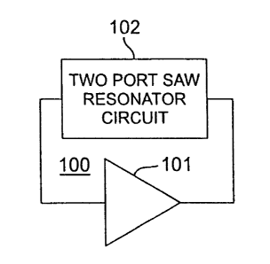
FIGURE 1 depicts a circuit diagram for an exemplary oscillator
including a two port tunable SAW resonator circuit according to one
embodiment of the present invention;
FIGURE 2A illustrates in greater detail a circuit diagram for
a two port SAW resonator circuit in the exemplary oscillator
according to one embodiment of the present invention;
FIGURE 2B illustrates in greater detail a circuit diagram for
a two port SAW resonator circuit in the exemplary oscillator
according to another embodiment of the present invention;
FIGURES 3A through 3D are frequency response plots
illustrating the operation of the two port SAW resonator circuit
according to one embodiment of the present invention;
FIGURE 4 is a circuit diagram of a single port SAW resonator
circuit for use in an oscillator; and
FIGURE 5 is a frequency response plot for a single port SAW
resonator circuit such as the one in FIGURE 4.
- 9 -
i I
CA 02375327 2002-03-08
ATTY. DOCKET NO. RFMI01-00213 PATENT
DETAILED DESCRIPTION OF THE INVENTION
FIGURES 1 through 3A-3D, discussed below, and the various
embodiments used to describe the principles of the present
invention in this patent document are by way of illustration only
and should not be construed in any way to limit the scope of the
invention. Those skilled in the art will understand that the
principles of the present invention may be implemented in any
suitably arranged device.
FIGURE 1 depicts a circuit diagram for an exemplary oscillator
including a two port tunable SAW resonator circuit according to one
embodiment of the present invention. Oscillator 100 maybe, for
example, a local oscillator within a SONET clock recovery circuit.
Oscillator 100 includes an amplifier 101 connected in a series loop
with a two port SAW resonator circuit 102, forming a Pierce
oscillator. Two port SAW resonator circuit 102 may have either
configuration shown in FIGURES 2A-2B.
FIGURE 2A illustrates in greater detail a circuit diagram for
a two port SAW resonator circuit in. the exemplary oscillator
according to one embodiment of the present invention. Two port SAW
resonator circuit 102 includes a two port SAW resonator 200,
depicted in FIGURE 2A by the equivalent circuit for the two port
- 10 -
I I
CA 02375327 2002-03-08
ATTY. DOCKET N0. RFMI01-00213 PATENT
SAW resonator within the frequency range of interest. The
equivalent circuit of the two port SAW resonator 200 within the
target frequency range includes a series resonator comprising a
motional inductance LM, a motional capacitance CM and a motional
resistance RM all connected in series. "Stray" capacitances Co, and
Co" formed by the internal parasitic and package capacitance (and
any other unintentional capacitance) of the SAW resonator as seen
from one of the ports of the SAW resonator 200, are connected
between the ends of the series resonator and ground.
To make the SAW resonator 200 tunable in the present
invention, two port SAW resonator circuit 102 includes inductances
Lol and La, coupled between the ports of the SAW resonator 200 and
ground, each inductance Lol and Log sized to effectively tune out
capacitances Col and Co" respectively. Variable tuning capacitances
C~l and C.~"r,,E2, which may be varactor diodes, are each connected in
series between one port of the SAW resonator 200 and either an
input port 2 O1 or an output port 2 02 f or the two port SAW resonator
circuit 102. With capacitances Col and Coy negated, either
capacitance C.L,,,r,El or C.~z alters the resonant frequency of the
series resonator. Accordingly, as the capacitance of tuning
capacitance (s) C~l and/or C~z decreases, the center frequency for
the passband of the two port SAW resonator circuit 102 increases.
- 11 -
.., i I
CA 02375327 2002-03-08
ATTY. DOCKET N0. RFMI01-00213 PATENT
The desired tune range is thereby achieved with--because a high Q
SAW device is employed--inherent low phase noise.
Prior art efforts to employ a SAW resonator within a local
oscillator failed to consider removing the stray capacitances Col
and Coy within the equivalent circuit of a SAW resonator to allow
access to the series resonant circuit within the equivalent circuit
for direct tuning of the SAW resonator. Instead, prior art efforts
at tuning SAW resonators have utilized tuning circuits which simply
tuned the overall circuit across the passband of the SAW device,
limiting tune range to the inherently narrow passband of the SAW
device.
To produce a high Q SAW device, the motional capacitance CM
should provide a high capacitive reactance, and therefore should be
a very small capacitance on the order of femptoFarads (fF). For
SONET clock recovery applications, some of which require a resonant
frequency of 622 megaHertz (MHz), a motional inductance LM on the
order of milliHenrys (mH) is required. The stray capacitances Col
and Coz are (both) typically on the order of 1-2 picoFarads (pF).
Accordingly, unless the stray capacitances Col and Co, are tuned out
by parallel inductances L~l and Log (i . a . , inductances Lol and La,
resonate with stray capacitances Col and Co, at the desired
operational frequency) as described above, efforts to directly tune
- 12 -
CA 02375327 2002-03-08
ATTY. DOCKET NO. RFMI01-00213 PATENT
the series resonator within the equivalent circuit of the SAW
resonator device 200 will have no effect on the motional
capacitance C" of the series resonator due to the difference in
magnitudes of the stray capacitances Cal and Caz and the motional
capacitance CH.
Inductances Lol and Log need not completely tune out stray
~capaci~tances Col and Coz, but instead need merely reduce the
magnitude of any residual stray capacitance to a level which is
insignificant when compared to the magnitude of the motional
capacitance CM. For some applications, use of inductance values
lower than that required for resonance can increase the tuning
range of the resonant circuit. The size of inductances I~l and Loz
are therefore noncritical, and manufacturing variances may be
tolerated. Those skilled in the art will further recognize that,
in lieu of shunt inductances Lol and Lo, as depicted in FIGURE 2A,
inductances may be connected in series with tuning capacitance C"",~l
between the input port 201 and SAW resonator 200, in series with
tuning capacitance C~~ between output port 202 and SAW resonator
200, or both. Such series connected-inductances will, if
appropriately sized, resonate with stray capacitances Col and Coz to
effectively tune out such stray capacitances and permit direct
access to the series resonator within the equivalent circuit for
- 13 -
i
CA 02375327 2002-03-08
ATTY. DOCKET N0. RFMI01-00213 PATENT
SAW resonator 200. Moreover, ~ combination of series-connected
and shunt inductances which, together, effectively tune out stray
capacitances may also be employed.
Although necessarily small to achieve the desired resonant
frequency and a high Q, the motional capacitance CM employed for a
single pole, two port SAW resonator 200 of the type disclosed
should be as large as possible to allow tuning capacitances C~1 or
C~~ to significantly impact the series resonator and provide
acceptable tune range. With a high impedance SAW resonator 200
l0 providing insertion loss on the order of 10 decibels (dB), the
required motional capacitance is too small to be tuned. However,
by utilizing an optimized, low impedance SAw resonator 200, the
same Q may be achieved using a larger motional capacitance CM. A
suitable value for the motional capacitance CM is approximately 0.6
fF for a 622 MIIz center frequency. A motional capacitance C" of
approximately half that value would significantly reduce the tune
range. For a motional capacitance CM of approximately 0.6 fF,
tuning capacitances C.~l or C.n,~, may have a tuning range of
approximately 2.0-0.4 pF.
FIGURE 2B illustrates in greater detail a circuit diagram for
a two port SAW resonator circuit in the exemplary oscillator
according to another embodiment of the.present invention. In this
- 14 -
i.Ai :: ~ -
CA 02375327 2002-03-08
ATTY. DOCKET N0. RFMI01-00213 PATENT
alternative embodiment, the two port SAW resonator circuit 102
contains only a single inductance Lol and a single tuning
capacitance C~1 at only one port of the SAW resonator 200. While
providing inductances Lo, and Lo, and tuning capacitances Cue, and
C~~ at both ports of the SAW resonator 200 as depicted in FIGURE
2 provides greater tune range, when SAW resonator circuit 102
-- - drives a load (not shown) of approximately 50-100 ohms (f2) or less
in parallel with stray capacitance Co" the impedance of stray
capacitance Co, becomes insignificant and the series resonator
within SAW resonator 200 may be tuned utilizing only a single
tuning capacitance C.j",,Fl at the input port for the SAW resonator
200. Accordingly, the second inductance Lo, and tuning capacitance
C~~ are optional. When not substantially tuned out with a
parallel inductance, however, stray capacitance Coy will continue
to prevent direct access to the series resonator within the
equivalent circuit for the SAW resonator 200 for direct tuning of
the resonant frequency using tuning capacitance C.~,~z.
While the alternative embodiment illustrates the inductance L~,
and tuning capacitance CT",,~, between the SAW resonator~200 and the
output port 202 being eliminated, with an appropriate input
impedance the inductance Lol and tuning capacitance C~1 between the
SAW resonator 200 and the input port 201 may be eliminated instead.
- 15 -
.~ .l l
CA 02375327 2002-03-08
ATTY. DOCKET NO. RFMI01-00213 PATENT
Whereas the prior art provides a tune range of perhaps 60 I~iz
in connection with a high Q SAW resonator, the present invention
with the component values described provides fox either embodiment
a tune range of at least approximately 400 KHz. For SONET clock
S recovery applications in which variances of up to 500 parts-per-
million (ppm) must be tolerated, the required tune range for a
center frequency of 622 MHz is approximately 300 KHz.
FIGURES 3A through 3D are frequency response plots
illustrating the operation of the two port SAW resonator according
to one embodiment of the present invention. The output amplitude
and phase for a tunable SAW resonator circuit of the type described
above are plotted for a 2.5 MHz range of freauencies centered on
622.2 MHz. The output amplitude 301 is plotted on a scale of 5
decibels (dB) per division, while the output phase 302 is plotted
on a linear scale of 90° per division.
In FIGURE 3A, the tuning voltage applied to varactor diodes
within the tunable SAW resonator circuit to adjust the capacitance
is zero. The resulting output signal amplitude has a center
frequency of 622.159375 MHz, a maximum signal amplitude of -7.4807
2 0 dH, and a phase of -48.219°. In FIGURE 3B, the tuning voltage
applied to the varactor diodes is increased to 2.5 volts (V),
moving the center frequency to 622.300000 MHz, the maximum signal
- 16.-
I I
CA 02375327 2002-03-08
ATTY. DOCKET NO. RFMI01-00213 PATENT
amplitude to -8.9772 dB, and the phase to -41.892°. The tuning
voltage applied to the varactor diodes for the plot in FIGURE 3C is
2.75 V, resulting in a center frequency of 622.340625 M~iz, a
maximum signal amplitude to -10.143 dB, and a phase of -40:601°.
Finally, the tuning voltage in FIGURE 3D is 3.0 V, the center
frequency is 622.380375 NO-iz, the maximum amplitude is -12.35 dB,
and the phase is -31.771°.
The SAW oscillator 100 of the present invention, which is a
voltage controlled SAW oscillator (VCSO), may be advantageously
employed within the phase lock loop (PLL) of a clock recovery
circuit, particularly for SONET applications. SAW oscillator 100
exhibits very low phase noise and edge fitter while providing
sufficient tune range to track slight changes (error) in frequency
during operation, allowing for manufacturing variances, and
accommodating temperature variations.
Although the present invention has been described in detail,
those skilled in the art should understand that they can make
various changes, substitutions and alterations herein without
departing from the spirit and scope of the invention in its
broadest form.
- 17 -